EP0868035A2 - Analoger Signalübertragungskreis - Google Patents
Analoger Signalübertragungskreis Download PDFInfo
- Publication number
- EP0868035A2 EP0868035A2 EP98105046A EP98105046A EP0868035A2 EP 0868035 A2 EP0868035 A2 EP 0868035A2 EP 98105046 A EP98105046 A EP 98105046A EP 98105046 A EP98105046 A EP 98105046A EP 0868035 A2 EP0868035 A2 EP 0868035A2
- Authority
- EP
- European Patent Office
- Prior art keywords
- positive
- negative
- input terminal
- differential amplifier
- terminal
- Prior art date
- Legal status (The legal status is an assumption and is not a legal conclusion. Google has not performed a legal analysis and makes no representation as to the accuracy of the status listed.)
- Withdrawn
Links
- 230000008054 signal transmission Effects 0.000 title claims abstract description 70
- 239000003990 capacitor Substances 0.000 claims abstract description 158
- 238000004804 winding Methods 0.000 claims description 40
- 230000006870 function Effects 0.000 description 22
- 238000010586 diagram Methods 0.000 description 21
- 230000010355 oscillation Effects 0.000 description 10
- 230000005540 biological transmission Effects 0.000 description 6
- 230000003321 amplification Effects 0.000 description 3
- 238000003199 nucleic acid amplification method Methods 0.000 description 3
- 238000005513 bias potential Methods 0.000 description 2
- 230000007423 decrease Effects 0.000 description 1
- 230000002265 prevention Effects 0.000 description 1
- 230000005236 sound signal Effects 0.000 description 1
- 230000001131 transforming effect Effects 0.000 description 1
Images


Classifications
-
- H—ELECTRICITY
- H04—ELECTRIC COMMUNICATION TECHNIQUE
- H04B—TRANSMISSION
- H04B3/00—Line transmission systems
- H04B3/02—Details
-
- H—ELECTRICITY
- H04—ELECTRIC COMMUNICATION TECHNIQUE
- H04B—TRANSMISSION
- H04B1/00—Details of transmission systems, not covered by a single one of groups H04B3/00 - H04B13/00; Details of transmission systems not characterised by the medium used for transmission
- H04B1/38—Transceivers, i.e. devices in which transmitter and receiver form a structural unit and in which at least one part is used for functions of transmitting and receiving
- H04B1/40—Circuits
- H04B1/54—Circuits using the same frequency for two directions of communication
- H04B1/58—Hybrid arrangements, i.e. arrangements for transition from single-path two-direction transmission to single-direction transmission on each of two paths or vice versa
- H04B1/583—Hybrid arrangements, i.e. arrangements for transition from single-path two-direction transmission to single-direction transmission on each of two paths or vice versa using a bridge network
-
- H—ELECTRICITY
- H04—ELECTRIC COMMUNICATION TECHNIQUE
- H04L—TRANSMISSION OF DIGITAL INFORMATION, e.g. TELEGRAPHIC COMMUNICATION
- H04L25/00—Baseband systems
- H04L25/02—Details ; arrangements for supplying electrical power along data transmission lines
- H04L25/0264—Arrangements for coupling to transmission lines
- H04L25/0266—Arrangements for providing Galvanic isolation, e.g. by means of magnetic or capacitive coupling
Definitions
- the present invention relates to an analog signal transmission circuit, and in particular to an analog signal transmission circuit in which a DC offset current is cut by polar capacitors.
- an analog signal transmission circuit provided in a modem or the like incorporates a drive circuit which has a transformer for transforming power and insulating the analog signal transmission circuit from an external circuit.
- the transformer is driven by a single-end type amplifier or a push-pull type amplifier (hereinafter referred to as a differential amplifier).
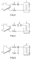
- FIG. 1 shows a conventional analog signal transmission circuit in which the transformer is driven by a differential amplifier 1.
- the amplifier 1 is a differential input/output type amplifier and has a positive output terminal 2 and a negative output terminal 3. Signals are supplied from the output terminals 2 and 3 to the transformer 6 through output resistors 4 and 5, respectively.
- the values of the output resistors 4 and 5 are determined so as to satisfy the impedance matching with the characteristic impedance of a communication circuit connected to secondary windings of the transformer 6.
- the output terminals 2 and 3 of the amplifier 1 are connected to the transformer 6 in a DC manner. In general, a DC voltage is superimposed on the output of the amplifier 1.
- the voltage between the output terminals 2 and 3 includes an error voltage referred to as "offset voltage".
- a DC offset current I flows due to the offset voltage as shown in FIG. 2.
- the offset current I flows through windings of the transformer 6.
- the offset voltage at the positive output terminal 2 is higher than that of the negative output terminal 3.
- the current flowing through the windings of the transformer 6 has the waveform shown in FIG. 3.
- the offset current I flows from the positive output terminal 2 to the negative output terminal 3 as indicated by arrows in FIG. 2.
- the offset current I flows from the negative output terminal 3 to the positive output terminal 2.
- FIG. 4 shows a conventional analog signal transmission circuit in which no offset current I flows through the windings of the transformer 6.
- the circuit has a capacitor 7 for cutting a direct current.
- the capacitor 7 prevents the offset current I from flowing through the windings of the transformer 6.
- the capacitor 7 is a non-polar one as in most analog signal transmission circuits. This is because which potential is higher, the potential at the positive output terminal 2 or the potential at the negative output terminal 3, depends on each analog signal transmission circuit.
- a circuit for processing low-frequency signals has a capacitor which has a large capacitance.
- a few kinds of non-polar capacitors, each having a large capacitance, are available.
- only a few kinds of non-polar capacitors, each having a capacitance of tens of microfarads ( ⁇ F) are available.
- polar capacitors are modified to be non-polar and used in most cases.
- FIG. 5 shows a conventional analog signal transmission circuit having two polar capacitors 8, not a non-polar capacitor.
- the two polar capacitors 8 are connected in serial and are non-polarized. They are connected at their negative-side terminals. They may be connected at their positive-side terminals.
- FIG. 6 shows a conventional analog signal transmission circuit which differs from the circuit shown in FIG. 5 in that the transformer 6 is connected between the capacitors 8. However, the circuit has the same advantage as the circuit shown in FIG. 5.
- One of the capacitors cannot perform its inherent function since a reverse DC voltage is applied to it. Thus, it cannot cut a DC offset current reliably. To be more specific, its capacitance decreases when a reverse voltage is applied to the capacitor. Thus, it is small, as compared with the case where a forward voltage is applied to the capacitor.
- the object of the present invention is to provide an analog signal transmission circuit which uses polar capacitors, and is designed such that a forward DC voltage is applied to the polar capacitors, ensuring the functions thereof.
- the analog signal transmission circuit of the present invention comprises a transformer, an amplifier for driving the transformer, and first and second polar capacitors which are connected in series such that those terminals of the first and second polar capacitors which have the same polarity are connected to each other, wherein the analog signal transmission circuit includes an element, which is connected between the terminals of the first and second polar capacitors which have the same polarity, for applying thereto a DC bias in accordance with the polarity of the terminals of the first and second polar capacitors.
- a predetermined DC bias is applied to the terminals of the first and second polar capacitors, and the potentials of the DC components at the terminals of the first and second capacitors are fixed at a DC bias potential. Therefore, the relationships between the DC offset potential of the output of the amplifier 1 and the potentials at the terminals of the first and second are the same as each other.
- a forward DC voltage can be applied to each of the first and second polar capacitors. Therefore, the polar capacitors can perform their inherent functions.
- the analog signal transmission circuit has a high performance.
- a resistor or an inductance element can be used as the element for applying a DC bias.
- the analog signal transmission circuit is designed such that a forward DC voltage is applied to the polar capacitors.
- the polar capacitors can perform their inherent functions.
- a device having the circuit of the present invention can operate reliably.
- FIG. 1 is a view showing the structure of a conventional analog signal transmission circuit.
- FIG. 2 is a view for explaining a DC offset current in the conventional analog signal transmission circuit.
- FIG. 3 is a view showing an output waveform of the conventional analog signal transmission circuit.
- FIG. 4 is a view showing the structure of another conventional analog signal transmission circuit.
- FIG. 5 is a view showing the structure of a further conventional analog signal transmission circuit.
- FIG. 6 is a view showing the structure of yet another conventional analog signal transmission circuit.
- FIG. 7 is a system block diagram of a computer system in which an analog signal transmission circuit according to the embodiment of the present invention is applied to a modem.
- FIG. 8 is a circuit diagram showing the structure of the analog signal transmission circuit according to the embodiment of the present invention.
- FIG. 9 is a view showing an output waveform of the analog signal transmission circuit according to the embodiment of the present invention.
- FIG. 10 is a circuit diagram showing a second example of the analog signal transmission circuit according to the embodiment of the present invention.
- FIG. 11 is a circuit diagram showing a third example of the analog signal transmission circuit according to the embodiment of the present invention.
- FIG. 12 is a circuit diagram showing a fourth example of the analog signal transmission circuit according to the embodiment of the present invention.
- FIG. 13 is a circuit diagram showing a fifth example of the analog signal transmission circuit according to the embodiment of the present invention.
- FIG. 14 is a circuit diagram showing a sixth example of the analog signal transmission circuit according to the embodiment of the present invention.
- FIG. 15 is a circuit diagram showing a seventh example of the analog signal transmission circuit according to the embodiment of the present invention.
- FIG. 16 is a circuit diagram showing an eighth example of the analog signal transmission circuit according to the embodiment of the present invention.
- FIG. 17 is a circuit diagram showing a ninth example of the analog signal transmission circuit according to the embodiment of the present invention.
- FIG. 18 is a circuit diagram showing a tenth example of the analog signal transmission circuit according to the embodiment of the present invention.
- FIG. 19 is a circuit diagram showing an eleventh example of the analog signal transmission circuit according to the embodiment of the present invention.
- FIG. 20 is a circuit diagram showing a twelfth example of the analog signal transmission circuit according to the embodiment of the present invention.
- FIG. 21 is a circuit diagram showing a thirteenth example of the analog signal transmission circuit according to the embodiment of the present invention.
- FIG. 22 is a circuit diagram showing a fourteenth example of the analog signal transmission circuit according to the embodiment of the present invention.
- FIG. 23 is a circuit diagram showing a fifteenth example of the analog signal transmission circuit according to the embodiment of the present invention.
- FIG. 24 is a circuit diagram showing a sixteenth example of the analog signal transmission circuit according to the embodiment of the present invention.
- FIG. 25 is a circuit diagram showing the first example of an operating point-determining circuit of an amplifier provided in the analog signal transmission circuit according to the embodiment of the present invention.
- FIG. 26 is a circuit diagram showing the second example of the operating point-determining circuit of the amplifier provided in the analog signal transmission circuit according to the embodiment of the present invention.
- FIG. 27 is a circuit diagram showing the third example of the operating point-determining circuit of the analog signal transmission circuit according to the embodiment of the present invention.
- FIG. 7 is a block diagram of a computer system in which an analog signal transmission circuit according to the embodiment of the present invention is applied to a modem circuit.
- the computer system shown in FIG. 7 has a system bus 10A and an inner bus 10B.
- the following structural elements are connected to the system bus 10A: a CPU 11 for controlling the computer system; a ROM (read-only memory) 12 in which a fixed program or the like is stored; a RAM (random-access memory) 13 constituting a main memory in which a program, a data or the like, to be processed, is stored; a DMAC (direct memory access controller) 14 for controlling direct memory access; a PIT (programmable interval timer) 16 which can be set according to a program; an RTC (real-time clock) 17 which is a clock module having a battery for use in operation; a backup RAM 19 serving as a data storing region having a resume function; an EBC (extension bus connector) 20 for use in extension of the function; a HDC (hard disc controller) 21 for interfacing a hard disc drive 43; an FDC (floppy disk controller) 22 for controlling a floppy disk drive 35; a print controller 23
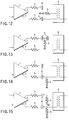
- FIG. 8 shows the structure of the analog signal transmission circuit according to the embodiment of the present invention which is applied to, e.g., the modem circuit 50 or the modem card 28 shown in FIG. 7.
- the analog signal transmission circuit is used as a hybrid circuit for enabling a four-wire transmission line to be used, in addition to a two-wire transmission line, in a modem or the like, and comprises a transmitter for transmitting an analog signal through an external two-wire communication line, and a receiver for receiving an analog signal externally sent through the external communication line.
- the transmitter comprises a differential amplifier 1, output resistors 4 and 5, two polar capacitors 8, and a resistor 9 for use in application of a DC bias.
- the receiver comprises a differential amplifier 101 for receiving and amplifying a signal externally transmitted through input resistors 104 and 105, resistors 102 and 103 for use in prevention of counterflow of a differential output from the differential amplifier 1, and resistors 106 and 107 for use in connection of a negative-feedback loop.
- one end of the resistor 9 is connected to a node at which those terminals of the two polar capacitors 8 which have the same polarity are connected to each other, and the other end of the resistor 9 is connected to a ground terminal AG.
- the analog signal transmission circuit shown in FIG. 8 is directed to the case where the DC offset voltages at output terminals 2 and 3 of the amplifier 1 are positive with respect to the potential of the ground terminal AG (hereinafter referred to as "ground potential").
- ground potential the negative-side terminals of the capacitors 8 are grounded through the resistor 9, and the potentials at the terminals 2 and 3 are positive.
- the capacitors 8 are forward-biased.
- each of the capacitors 8 When an AC analog signal is output from the differential amplifier 1, the positive side of each of the capacitors 8 performs an oscillation function on the basis of a DC potential of the output of the amplifier 1, and the negative side of each capacitor 8 performs an oscillation function on the basis of the ground potential.
- the capacitors 8 cut the DC components of the positive voltages at the output terminals 2 and 3. Thus, a direct current is prevented from flowing through the windings of the transformer 6, and the output waveform of the windings is obtained as shown in FIG. 9.
- the polar capacitors 8 are connected such that those terminals of the capacitors 8 which have the same polarity face each other, and are forward-biased, ensuring the inherent functions of the capacitors 8. Therefore, a device having the analog signal transmission circuit can operate reliably.
- the following advantage can be obtained:
- the capacitors 8 and the resistor 9 are located in a small region. In other words, a DC bias circuit comprising the capacitors 8 and the resistor 9 is small. As a result, the analog signal transmission circuit is also small.
- FIG. 10 shown the second example of the transmitter provided in the analog signal transmission circuit according to the embodiment of the present invention.
- the two polar capacitors 8 are connected in series through the windings of the transformer 6 such that those terminals of the capacitors 8 which have the same polarity are connected to each other.
- One end of the resistor 9 is connected to a node at which one of the windings of the transformer 6 is connected to the negative side of one of the capacitors 8 which is connected to the negative output terminal 3 of the differential amplifier 1.
- the other end of the resistor 9 is connected to the ground terminal AG.
- the second example is also directed to the case where the DC voltages at the output terminals 2 and 3 of the amplifier 1 are positive with respect to the ground potential.
- the potential of the DC component at the negative side of each capacitor 8 is held at the ground potential by the resistor 9.
- the output terminals 2 and 3 are positive, and thus the capacitors 8 are forward-biased.
- each capacitor 8 When a DC analog signal is output from the differential amplifier 1, the positive side of each capacitor 8 performs an oscillation function on the basis of a DC potential of the output of the amplifier 1, and the negative side of each capacitor 8 performs an oscillation function on the basis of the ground potential.
- a direct current is prevented from flowing through the windings of the transformer 6 since the DC components of the positive voltages at the output terminals 2 and 3 are cut.
- the transmitter shown in FIG. 10 as well as the transmitter shown in FIG. 8, ensures the inherent functions of the capacitors 8 since the capacitors 8 are forward-biased.
- a device having the transmitter of FIG. 10 can operate reliably.
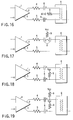
- FIG. 11 shows the third example of the transmitter provided in the analog signal transmission circuit according to the embodiment of the present invention.
- the ends of two resistors 9 having the same value are respectively connected to the negative-side terminals of the two polar capacitors 8.
- the other ends of the resistors 9 are connected to the ground terminal AG.
- the third example is also directed to the case where the DC voltages at the output terminals 2 and 3 are positive with respect to the ground potential.
- the number of resistors is larger than that of resistors provided in each of the transmitters shown in FIGS. 8 and 10, in order to more balance the AC component.
- a noise is applied to only one end side of the windings of the transformer 6 through the resistor 9, when the ground potential varies.
- the noise is transmitted to a communication line as a normal mode noise which varies only the potential of one of the two wire paths of a two-wire transmission line, since the transformer 6 is not balanced with respect to the ground terminal AG.
- the normal mode noise is an undesirable noise for communication.
- FIG. 12 shows the fourth example of the transmitter provided in the analog signal transmission circuit according to the embodiment of the present invention.
- the transformer 6 and the resistor 9 are connected between the negative sides of the two polar capacitors 8.
- One end of the resistor 9 is connected to a tap of the transformer 6, and the other end of the resistor 9 is connected to the ground terminal AG.
- the fourth example is also directed to the case where the DC voltages at the output terminals 2 and 3 are positive with respect to the ground potential.
- the tap of the transformer 6 is located at a middle point of the windings, balancing the AC component as in the transmitter shown in FIG. 11.
- a common mode noise is applied to the transformer 6 through the resistor 9, and a common mode noise component is eliminated due to the common mode component-eliminating function of the transformer 6. As a result, no noise is transmitted to the communication line.
- FIG. 13 shows the fifth example of the transmitter provided in the analog signal transmission circuit according to the embodiment of the present invention.
- the positive-side terminals of the two polar capacitors 8 are connected to each other.
- One end of the resistor 9 is connected to a node at which the capacitors 8 are connected to each other, and the other end of the resistor 9 is connected to the ground terminal AG.
- the transmitter of the fifth example corresponds to the transmitter shown in FIG. 8. However, unlike the transmitter of FIG. 8, the transmitter of the fifth example is directed to the case where the DC voltages at the output terminals 2 and 3 are negative with respect to the ground potential. Thus, the potentials of the DC components at the positive sides of the two polar capacitors 8 are held at the ground potential by the resistor 9.
- the capacitors 8 are forward-biased since the potentials of the output terminals 2 and 3 are negative.
- each capacitor 8 When a DC analog signal is output from the differential amplifier 1, the negative side of each capacitor 8 performs an oscillation function on the basis of the DC potential of the output of the amplifier 1, and the positive side of each capacitor 8 performs an oscillation function on the basis of the ground potential.
- a direct current is prevented from flowing through the windings of the transformer 6 since the DC components of the negative voltages at the output terminals 2 and 3 are cut.
- FIG. 14 shows the sixth example of the transmitter provided in the analog signal transmission circuit according to the embodiment of the present invention.
- the positive-side terminals of the two polar capacitors 8 are connected through the transformer 6.
- One end of the resistor 9 is connected to the positive-side terminal of one of the capacitors 8 which is connected to the negative output terminal 3.
- the other end of the resistor 9 is connected to the ground terminal AG.
- This example is also directed to the case where the DC voltages at the output terminals 2 and 3 are negative with respect to the ground potential.
- the potentials of the DC components at the positive sides of the capacitors 8 are held at the ground potential by the resistor 9.
- the capacitors 8 are forward-biased since the potentials of the output terminals 2 and 3 are negative.
- each capacitor 8 When a DC analog signal is output from the differential amplifier 1, the negative side of each capacitor 8 performs an oscillation function on the basis of the DC potential of the output of the amplifier 1, and the positive side of each capacitor 8 performs an oscillation function on the basis of the ground potential.
- a direct current is prevented from flowing through the windings of the transformer 6 since the DC components of the negative voltages at the output terminals 2 and 3 are cut.
- the capacitors 8 are forward-biased as in the transmitter of FIG. 13 (the fifth example), ensuring the inherent functions of the capacitors 8.
- a device having the transmitter of the sixth example can operate reliably.
- FIG. 15 shows the seventh example of the transmitter provided in the analog signal transmission circuit according to the embodiment of the present invention.
- the ends of the resistors 9 having the same value are respectively connected to the positive-side terminals of the two polar capacitors 8.
- the other ends of the resistors 9 are connected to the ground terminals AG.
- This example is also directed to the case where the DC voltages at the output terminals 2 and 3 are negative with respect to the ground potentials.
- the number of resistors is larger than that of resistors provided in the transmitter shown in each of FIGS. 13 and 14, in order to more balance the AC component.
- FIG. 16 shows the eighth example of the transmitter provided in the analog signal transmission circuit according to the embodiment of the present invention.
- the transformer 6 and the resistor 9 are connected between the positive-side terminals of the two polar capacitors 8.
- One end of the resistor 9 is connected to the tap of the transformer 6, and the other end of the resistor 9 is connected to the ground terminal AG.
- This example is also directed to the case where the DC voltages at the output terminals 2 and 3 are negative with respect to the ground potential.
- the tap is located at a middle point of the windings, balancing the AC component as in the transmitter shown in FIG. 15.
- a common mode noise is applied to the transformer 6 through the resistor 9, and a common mode component is eliminated due to the common mode component-eliminating function of the transformer 6. As a result, no noise is transmitted to the communication line.
- FIG. 17 shows the ninth example of the transmitter provided in the analog signal transmission circuit according to the embodiment of the present invention.
- one end of the resistor 9 is connected to the connecting point of the two polar capacitors 8, and the other end of the resistor 9 is connected to a positive power supply Vcc.
- This example is directed to the case where the DC voltages at the output terminals 2 and 3 are negative with respect to the potential of the power supply Vcc.
- the potentials of the DC components at the positive sides of the capacitors 8 are held at the ground potential.
- the capacitors 8 are forward-biased since the potentials of the output terminals 2 and 3 are negative.
- FIG. 18 shows the tenth example of the transmitter provided in the analog signal transmission circuit according to the embodiment of the present invention.
- the positive-side terminals of the two polar capacitors 8 are connected through the transformer 6.
- One end of the resistor 9 is connected to the positive-side terminal of one of the capacitors 8 which is connected to the output terminal 3 of the amplifier 1, and the other end of the resistor 9 is connected to the positive power supply Vcc.
- This example is also directed to the case where the DC voltages at the output terminals 2 and 3 are negative with respect to the potential of the power supply Vcc.
- the potentials of the DC components at the positive sides of the capacitors 8 are held at the potential of the positive power supply Vcc.
- the capacitors 8 are forward-biased since the potentials at the output terminals 2 and 3 are negative.
- FIG. 19 shows the eleventh example of the transmitter provided in the analog signal transmission circuit according to the embodiment of the present invention.
- the positive-side terminals of the two polar capacitors 8 are connected through the transformer 6.
- the ends of the resistors 9 are respectively connected to the capacitors 8, and the other ends of the resistors 9 are connected to the positive power supplies Vcc.
- This example is also directed to the case where the DC voltages at the output terminals 2 and 3 are negative with respect to the potential of the power supplies VCC.
- the number of resistors is larger than that of resistors provided in the transmitter shown in each of FIGS. 17 and 18, in order to more balance the AC component.
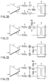
- FIG. 20 shows the twelfth example of the transmitter provided in the analog signal transmission circuit according to the embodiment of the present invention.
- the transformer 6 and the resistor 9 are connected between the positive-side terminals of the two polar capacitors 8.
- One end of the resistor 9 is connected to the tap of the transformer 6, and the other end of the resistor 9 is connected to the positive power supply Vcc.
- This example is also directed to the case where the DC voltages at the output terminals 2 and 3 are negative with respect to the potential of the power supply Vcc.
- the tap is located at a middle point of the windings, balancing the AC component as in the transmitter shown in FIG. 19.
- a common mode noise is applied to the transformer 6 through the resistor 9, and a common mode noise component is eliminated by the transformer 6. As a result, no noise is transmitted to the communication line.
- FIG. 21 shows the thirteenth example of the transmitter provided in the analog signal transmission circuit according to the embodiment of the present invention.
- one end of the resistor 9 is connected to a node at which the two polar capacitors 8 are connected to each other, and the other end of the resistor 9 is connected to a negative power supply Vss.
- This example is also directed to the case where the DC voltages at the output terminals 2 and 3 are negative with respect to the potential of the negative power supply Vss.
- the potentials of the DC components at the negative sides of the capacitors 8 are held at the potential of the negative power supply Vss.
- the capacitors 8 are forward-biased since the potentials at the output terminals 2 and 3 are positive.
- each capacitor 8 When a DC analog signal is output from the differential amplifier 1, the positive side of each capacitor 8 performs an oscillation function on the basis of the DC potential of the output of the amplifier 1, and the negative side of each capacitor 8 performs an oscillation function on the basis of the negative power supply potential.
- a direct current is prevented from flowing through the windings of the transformer 6 since the capacitors 8 cut the DC components of the positive voltages at the output terminals 2 and 3.
- FIG. 22 shows the fourteenth example of the transmitter provided in the analog signal transmission circuit according to the embodiment of the present invention.
- the negative-side terminals of the capacitors 8 are connected through the transformer 6.
- One end of the resistor 9 is connected to a node at which the transformer 6 is connected to the negative-side terminal of one of the capacitors 8 which is connected to the output terminal 3, and the other end of the resistor 9 is connected to the negative power supply Vss.
- This example is also directed to the case where the DC voltages at the output terminals 2 and 3 are positive with respect to the potential of the power supply Vss.
- the potentials of the DC components at the negative sides of the capacitors 8 are held at the potential of the negative power supply Vss by the resistor 9.
- the capacitors 8 are forward-biased since the potentials at the output terminals 2 and 3 are positive.
- FIG. 23 shows the fifteenth example of the transmitter provided in the analog signal transmission circuit according to the embodiment of the present invention.
- the negative-side terminals of the two polar capacitors 8 are connected through the transformer 6.
- the ends of the resistors 9 are respectively connected to the negative-side terminals of the capacitors 8, and the other ends of the resistors 9 are connected to the negative power supplies Vss.
- This example is also directed to the case where the DC voltages at the output terminals 2 and 3 are positive with respect to the potential of the power supplies Vss.
- the number of resistors is larger than that of resistors provided in the transmitter shown in each of FIGS. 21 and 22, in order to more balance the AC component.
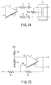
- FIG. 24 shows the sixteenth example of the transmitter provided in the analog signal transmission circuit according to the embodiment of the present invention.
- the transformer 6 and the resistor 9 are connected between the negative-side terminals of the two polar capacitors 8.
- One end of the resistor 9 is connected to the tap of the transformer 6, and the other end of the resistor 9 is connected to the negative power supply Vss.
- This example is also directed to the case where the DC voltages at the output terminals 2 and 3 are positive with respect to the potential of the power supply Vss.
- the tap is located at a middle point of the windings, balancing the AC component as in the transmitter shown in FIG. 23.
- a common mode noise is applied to the transformer 6 through the resistor 9, and a common mode noise component is eliminated by the transformer 6. As a result, no noise is transmitted to the communication line.
- FIG. 25 shows a circuit for applying a positive DC voltage to the output terminals 2 and 3 provided in each of the transmitters shown in FIGS. 8, 10 to 12 and 21 to 24.
- a voltage dividing circuit comprising resistors 10 and 11 generates an optional positive voltage by dividing the potential of the power supply Vcc and the ground potential.
- the positive voltage is applied to a positive input terminal 14 of the amplifier 1.
- the operating point of the amplifier 1 is determined, and the output terminals 2 and 3 have the aforementioned positive voltages, and thus has DC operating point-potentials.
- a negative-feedback resistor 12 is connected to a negative input terminal 15 and the positive output terminal 2.
- An input resistor 13 is connected to the negative input terminal 15.
- the amplification degree of the amplifier 1 depends on the total values of the negative-feedback resistor 12 and the input resistor 13.
- FIG. 26 shows a circuit for applying a negative DC voltage to the output terminals 2 and 3 provided in each of the transmitters shown in each of FIGS. 8, 10-12, and 21-24.
- the voltage dividing circuit comprising the resistors 10 and 11 generates an optional negative voltage by dividing the potential of the negative power supply Vss and the potential of the ground terminal AG.
- the negative voltage is applied to the positive input terminal 14 of the amplifier 1. Thereby, the operating point of the amplifier 1 is determined, and the output terminals 2 and 3 have the above negative voltages, and thus have DC operating point-potentials.
- the negative-feedback resistor 12 is connected to the negative input terminal 15 and the positive output terminal 2.
- the input resistor 13 is connected to the negative input terminal 15.
- the amplification degree of the amplifier 1 depends on the total values of the negative-feedback resistor 12 and the input resistor 13.
- FIG. 27 shows a circuit for applying the potential of the ground terminal AG to the output terminals 2 and 3.
- the circuit can be applied to the transmitter shown in each of FIGS. 17, and 21-24 as means for applying a bias.
- the positive input terminal 14 of the amplifier 1 is connected to the ground terminal AG. Thereby, the operating point of the amplifier 1 is determined, and each of the output terminals 2 and 3 has the ground potential, and thus has a DC operating point potential.
- the negative-feedback resistor 12 is connected to the negative input terminal 15 and the positive output terminal 2.
- the input resistor 13 is connected to the negative input terminal 15.
- the amplification degree of the amplifier 1 depends on the total value of the negative-feedback resistor 12 and the input resistor 13.
- a predetermined DC bias is applied to those terminals of the two polar capacitors 8 which have the same polarity.
- the potentials of the DC components at the terminals are fixed at the DC bias potential. Therefore, the relationship between the potential at one of the terminals and the DC offset potential of the output of the amplifier 1 is the same as that between the potential of the other and the DC offset potential of the output of the amplifier 1.
- a forward DC voltage can be applied to each of the capacitors 8. Therefore, the capacitors 8 can perform their inherent functions. Thus, the resultant circuit has a high performance.
- the analog signal transmission circuit according to the embodiment of the present invention is utilized as a line interface circuit (hybrid circuit) of a modem.
- the characteristic impedance of the line is 600 ohm. Therefore, in the embodiment of the present invention, the values of the resistors 4 and 5 are set such that the impedance of the modem including the transformer 6 is 600 ohm.
- the value of each of the resistors 4 and 5 is set to be 300 ohm if a transformer is used which has a sufficient inductance and windings having a turns ratio of 1 to 1.
- the optimal values of the resistors 4 and 5 are determined in accordance with the characteristics of the amplifier 1 and transformer 6.
- a four-wire communication line used for the user, as well as a two-wire communication line for a specific use, may be used as the aforementioned communication line.
- the resistors 4 and 5 may be omitted, and may be replaced with a jumper wire having 0 ohm. Furthermore, the present invention can also be applied to the transmission of an audio signal.
- the resistor is used as the element for applying a DC bias.
- the inductance element may be used as the element for applying a DC bias, instead of the resistor.
- the resistance value of the DC component of the inductance element is 0 ohm.
- the inductance element is featured in that the resistance value of the AC component is sufficient for a frequency of a signal used in the circuit.
- the capacitors 8 may be located in any position on the path extending from the output terminal 2 to the output terminal 3, if they are connected in series such that the terminals having the same polarity are connected to each other. For example, in the analog signal transmission circuit shown in FIG. 8, even if the two polar capacitors 8 are connected in series such that the output resistor 4 is provided between them, the same advantage is obtained.
- the resistor 9 may be located in any position of the path between the capacitors 8.
- the number of capacitors 8 is not limited to two. It sometimes exceeds two in order that the capacitors 8 have a desired total capacitance. In this case, the capacitors 8 are connected either in series or in parallel.
- the number of resistors 9 is not limited to one.
Landscapes
- Engineering & Computer Science (AREA)
- Computer Networks & Wireless Communication (AREA)
- Signal Processing (AREA)
- Power Engineering (AREA)
- Amplifiers (AREA)
- Cable Transmission Systems, Equalization Of Radio And Reduction Of Echo (AREA)
Applications Claiming Priority (2)
| Application Number | Priority Date | Filing Date | Title |
|---|---|---|---|
| JP9075187A JPH10271043A (ja) | 1997-03-27 | 1997-03-27 | アナログ信号伝送回路 |
| JP75187/97 | 1997-03-27 |
Publications (1)
| Publication Number | Publication Date |
|---|---|
| EP0868035A2 true EP0868035A2 (de) | 1998-09-30 |
Family
ID=13568957
Family Applications (1)
| Application Number | Title | Priority Date | Filing Date |
|---|---|---|---|
| EP98105046A Withdrawn EP0868035A2 (de) | 1997-03-27 | 1998-03-19 | Analoger Signalübertragungskreis |
Country Status (3)
| Country | Link |
|---|---|
| US (1) | US5982215A (de) |
| EP (1) | EP0868035A2 (de) |
| JP (1) | JPH10271043A (de) |
Cited By (5)
| Publication number | Priority date | Publication date | Assignee | Title |
|---|---|---|---|---|
| EP1195913A1 (de) * | 2000-10-05 | 2002-04-10 | Alcatel | Verstärkervorrichtung |
| WO2002065662A3 (en) * | 2001-02-01 | 2003-12-11 | Analog Devices Inc | Line interface a matching impedance coupled ro a feedback path |
| EP1168740A3 (de) * | 2000-06-20 | 2004-01-14 | STMicroelectronics, Inc. | Leitungstreiber mit adaptiver Impedanz |
| DE19953219B4 (de) * | 1998-11-23 | 2007-03-15 | National Semiconductor Corp.(N.D.Ges.D.Staates Delaware), Santa Clara | Vorrichtung mit einer Differentialstrom-Steuerschaltung |
| CN103067079A (zh) * | 2013-01-06 | 2013-04-24 | 富通集团有限公司 | 一种光纤形变信号处理电路 |
Families Citing this family (6)
| Publication number | Priority date | Publication date | Assignee | Title |
|---|---|---|---|---|
| CN1205747C (zh) * | 2000-06-01 | 2005-06-08 | 皇家菲利浦电子有限公司 | 射频电路 |
| WO2002102047A2 (en) * | 2001-06-08 | 2002-12-19 | Broadcom Corporation | Integrated upstream amplifier for cable modems and cable set-top boxes |
| DE102004057094B4 (de) * | 2004-11-25 | 2020-12-24 | Avantgarde Acoustic Lautsprechersysteme Gmbh | Kapazitives Element |
| US7738565B1 (en) * | 2006-03-30 | 2010-06-15 | Magnetic Recording Solutions, Inc. | Peak detector |
| US8049537B2 (en) * | 2008-08-12 | 2011-11-01 | Marvell International Ltd. | Method and apparatus for reducing transmitter AC-coupling droop |
| KR101699233B1 (ko) * | 2015-03-31 | 2017-01-24 | (주)미라클인 | 전해장치용 전원공급회로 및 이를 포함하는 전해장치 |
Family Cites Families (4)
| Publication number | Priority date | Publication date | Assignee | Title |
|---|---|---|---|---|
| US5043598A (en) * | 1988-09-20 | 1991-08-27 | Tdk Corporation | High voltage supply having a voltage stabilizer |
| JPH0464839A (ja) * | 1990-07-03 | 1992-02-28 | Shinko Kogyo Co Ltd | 蓄熱式冷却方法 |
| US5570276A (en) * | 1993-11-15 | 1996-10-29 | Optimun Power Conversion, Inc. | Switching converter with open-loop input voltage regulation on primary side and closed-loop load regulation on secondary side |
| US5708377A (en) * | 1996-02-23 | 1998-01-13 | Wiltron Company | Low power dual sampler utilizing step recovery diodes (SRDS) |
-
1997
- 1997-03-27 JP JP9075187A patent/JPH10271043A/ja active Pending
-
1998
- 1998-03-19 EP EP98105046A patent/EP0868035A2/de not_active Withdrawn
- 1998-03-20 US US09/044,937 patent/US5982215A/en not_active Expired - Fee Related
Cited By (8)
| Publication number | Priority date | Publication date | Assignee | Title |
|---|---|---|---|---|
| DE19953219B4 (de) * | 1998-11-23 | 2007-03-15 | National Semiconductor Corp.(N.D.Ges.D.Staates Delaware), Santa Clara | Vorrichtung mit einer Differentialstrom-Steuerschaltung |
| EP1168740A3 (de) * | 2000-06-20 | 2004-01-14 | STMicroelectronics, Inc. | Leitungstreiber mit adaptiver Impedanz |
| EP1195913A1 (de) * | 2000-10-05 | 2002-04-10 | Alcatel | Verstärkervorrichtung |
| US6829352B2 (en) | 2000-10-05 | 2004-12-07 | Alcatel | Amplifier arrangement |
| WO2002065662A3 (en) * | 2001-02-01 | 2003-12-11 | Analog Devices Inc | Line interface a matching impedance coupled ro a feedback path |
| US6925172B2 (en) | 2001-02-01 | 2005-08-02 | Analog Devices, Inc. | Line interface with gain feedback coupled matching impedance |
| CN103067079A (zh) * | 2013-01-06 | 2013-04-24 | 富通集团有限公司 | 一种光纤形变信号处理电路 |
| CN103067079B (zh) * | 2013-01-06 | 2016-08-10 | 富通集团有限公司 | 一种光纤形变信号处理电路 |
Also Published As
| Publication number | Publication date |
|---|---|
| JPH10271043A (ja) | 1998-10-09 |
| US5982215A (en) | 1999-11-09 |
Similar Documents
| Publication | Publication Date | Title |
|---|---|---|
| US5856758A (en) | Low distortion driver employing positive feedback for reducing power loss in output impedance that effectively matches the impedance of driven line | |
| US5982215A (en) | Analog signal transmission circuit | |
| US4534039A (en) | Dataset powered by control and data signals from data terminal | |
| CN100525263C (zh) | 用于具有匹配阻抗的差分线路的终端对 | |
| US4734919A (en) | Circuit for serial data communication and power transmission | |
| US6507223B2 (en) | Differential line driver having adjustable common mode operation | |
| JPH07235952A (ja) | 信号伝送回路およびその回路を用いた信号伝送装置 | |
| US6925172B2 (en) | Line interface with gain feedback coupled matching impedance | |
| JP2936527B2 (ja) | バイアス回路 | |
| GB2152331A (en) | Pulse/direct current multiplexing circuit in key telephone system | |
| US7577205B1 (en) | Return-loss compliant DSL modem line interface unit with complex termination | |
| US20040183584A1 (en) | Communications device powered from host apparatus | |
| JP4443392B2 (ja) | 送信切り換え回路および半導体集積回路 | |
| CN100372243C (zh) | 双向通信系统 | |
| US6163165A (en) | Method for operating an information handling system | |
| US20060152275A1 (en) | Signal transmitting circuit | |
| JPH0661836A (ja) | 終端回路及び波形整形回路 | |
| US7308209B2 (en) | Transmitter circuit comprising a light source and a communication system | |
| US6330276B1 (en) | Transmission level setting circuit and modem unit using the same | |
| US7154954B1 (en) | Communication system | |
| JPH04154203A (ja) | ノイズフィルタ | |
| JPH0628073A (ja) | 終端抵抗回路 | |
| JPH03216045A (ja) | Acカップリング受信回路 | |
| JP3343091B2 (ja) | 通信システム | |
| JPH04243329A (ja) | 伝送回路 |
Legal Events
| Date | Code | Title | Description |
|---|---|---|---|
| PUAI | Public reference made under article 153(3) epc to a published international application that has entered the european phase |
Free format text: ORIGINAL CODE: 0009012 |
|
| 17P | Request for examination filed |
Effective date: 19980416 |
|
| AK | Designated contracting states |
Kind code of ref document: A2 Designated state(s): AT BE CH DE DK ES FI FR GB GR IE IT LI LU MC NL PT SE |
|
| AX | Request for extension of the european patent |
Free format text: AL;LT;LV;MK;RO;SI |
|
| STAA | Information on the status of an ep patent application or granted ep patent |
Free format text: STATUS: THE APPLICATION HAS BEEN WITHDRAWN |
|
| 18W | Application withdrawn |
Withdrawal date: 19981028 |