EP0809353B1 - Amplifier for cancelling noise between circuit systems - Google Patents
Amplifier for cancelling noise between circuit systems Download PDFInfo
- Publication number
- EP0809353B1 EP0809353B1 EP97107186A EP97107186A EP0809353B1 EP 0809353 B1 EP0809353 B1 EP 0809353B1 EP 97107186 A EP97107186 A EP 97107186A EP 97107186 A EP97107186 A EP 97107186A EP 0809353 B1 EP0809353 B1 EP 0809353B1
- Authority
- EP
- European Patent Office
- Prior art keywords
- circuit
- amplifier
- reference potential
- input terminal
- resistor
- Prior art date
- Legal status (The legal status is an assumption and is not a legal conclusion. Google has not performed a legal analysis and makes no representation as to the accuracy of the status listed.)
- Expired - Lifetime
Links
Images


Classifications
-
- H—ELECTRICITY
- H03—ELECTRONIC CIRCUITRY
- H03L—AUTOMATIC CONTROL, STARTING, SYNCHRONISATION, OR STABILISATION OF GENERATORS OF ELECTRONIC OSCILLATIONS OR PULSES
- H03L7/00—Automatic control of frequency or phase; Synchronisation
-
- H—ELECTRICITY
- H03—ELECTRONIC CIRCUITRY
- H03F—AMPLIFIERS
- H03F1/00—Details of amplifiers with only discharge tubes, only semiconductor devices or only unspecified devices as amplifying elements
- H03F1/26—Modifications of amplifiers to reduce influence of noise generated by amplifying elements
-
- H—ELECTRICITY
- H03—ELECTRONIC CIRCUITRY
- H03F—AMPLIFIERS
- H03F3/00—Amplifiers with only discharge tubes or only semiconductor devices as amplifying elements
- H03F3/45—Differential amplifiers
- H03F3/45071—Differential amplifiers with semiconductor devices only
- H03F3/45076—Differential amplifiers with semiconductor devices only characterised by the way of implementation of the active amplifying circuit in the differential amplifier
- H03F3/45475—Differential amplifiers with semiconductor devices only characterised by the way of implementation of the active amplifying circuit in the differential amplifier using IC blocks as the active amplifying circuit
-
- H—ELECTRICITY
- H03—ELECTRONIC CIRCUITRY
- H03F—AMPLIFIERS
- H03F3/00—Amplifiers with only discharge tubes or only semiconductor devices as amplifying elements
- H03F3/45—Differential amplifiers
- H03F3/45071—Differential amplifiers with semiconductor devices only
- H03F3/45479—Differential amplifiers with semiconductor devices only characterised by the way of common mode signal rejection
- H03F3/45928—Differential amplifiers with semiconductor devices only characterised by the way of common mode signal rejection using IC blocks as the active amplifying circuit
- H03F3/45968—Differential amplifiers with semiconductor devices only characterised by the way of common mode signal rejection using IC blocks as the active amplifying circuit by offset reduction
- H03F3/45973—Differential amplifiers with semiconductor devices only characterised by the way of common mode signal rejection using IC blocks as the active amplifying circuit by offset reduction by using a feedback circuit
-
- H—ELECTRICITY
- H03—ELECTRONIC CIRCUITRY
- H03F—AMPLIFIERS
- H03F2200/00—Indexing scheme relating to amplifiers
- H03F2200/189—Indexing scheme relating to amplifiers the ground, reference or shield potential difference between different chips being controlled
-
- H—ELECTRICITY
- H03—ELECTRONIC CIRCUITRY
- H03F—AMPLIFIERS
- H03F2200/00—Indexing scheme relating to amplifiers
- H03F2200/372—Noise reduction and elimination in amplifier
Definitions
- the present invention relates to an amplifier for canceling noise generated between circuit systems, and particularly to an analog amplifier, which is applied to, for example, an audio circuit, for preventing noise from being generated to an analog output signal to be sent to the other systems having a different reference potential based on a difference between two circuit systems in the reference potential.
- the circuit is formed on a plurality of circuit boards, and these plurality of circuit systems are connected by a connection line.
- the connection line In the case of connecting the reference potentials, e.g., ground potentials, of different circuit systems, by the connection line, there occurs a case in which a current flows between the reference potentials or a case in which the connection line acts as an antenna to cause noise to be carried on the connection line.
- a potential difference occurs between the reference potentials of the different circuit systems.
- the potential difference generally includes an unfavorable noise component. As a result, particularly, the analog circuit is largely damaged.
- FIG. 15 shows a mechanism in which noise is generated between reference potentials of two circuit systems each formed on a different circuit boards, that is, ground potentials.
- Arrows illustrated between two circuit systems 111 and 112 show a direction where a signal is received and transmitted. It is assumed that the total amount of current I1 flows in transmitting a signal from the first circuit system 111 to the second signal system 112 and that the total amount of current 12 flows in transmitting a signal from the second circuit system 112 to the first circuit system 111. As a result, the current of I1 - I2 flows into a connection line between reference potentials 113 and 114 of two circuit boards in a direction from the first circuit system 111 to the second circuit system 112.
- connection line serves as an antenna
- a current In which is generated by noise to enter in a form of a radio wave
- currents I1 and I2 are surely generated in receiving and transmitting the signal.
- the current I1 and I2 are increased as the system is enlarged and the number of digital circuits is increased.
- the current In is also increased as the number of the digital circuits is increased, unnecessary amount of radiation is increased and the reference potential connection line becomes long.
- impedance Z is also increased as the connection line between the reference potentials becomes long. Therefore, it can be considered that the reference potential difference Vx becomes large as the scale of the system and the digital section of the system become large.
- the DC component of the reference potential difference Vx can be cut by a coupling condenser.
- the AC component is superimposed on the signal component in receiving and transmitting the analog signal. As a result, transmission property is deteriorated.
- FIG. 14 shows one example of such a signal receiving and transmitting circuit.
- This type of the signal receiving and transmitting circuit comprises an amplifier, a differential amplifier 104, and two signal lines.
- the amplifier is provided at an output stage of the first circuit system 111 of the signal output side.
- the amplifier comprises inverting type analog amplifiers 101, 102, and 103 for generating differential signals eo+ and eo- of a signal eil to be transmitted.
- the differential amplifier 104 is provided at an input stage of the second circuit system 112 of the signal input side.
- the differential signals eo+ and eo- are input to the differential amplifier 104.
- Two signal lines transmit the differential signals.
- This type of the circuit transmits the signal in the form of a differential signal, and receives the signal in the form of a differential signal.
- an output potential eo2 of the differential amplifier 104 can be obtained as follows.
- noise Vx can be prevented from appearing in the output potential eo2.
- EP-0 482 291 discloses an isolator circuit for an audio system having an operational amplifier provided between a signal source and an amplifier. A capacitor and a resistor connected in series are connected between each input of the operational amplifier and the signal source. A buffer amplifier is provided between the capacitor and the resistor of each input line of the operational amplifier.
- An object of the present invention is to provide a circuit for receiving and transmitting a signal without an increasing manufacturing cost and a circuit occupying area and generating a noise component.
- the object can be achieved by the following structure.
- FIG. 1 shows an embodiment of the present invention.
- the same reference numerals are added to the structural elements in common to each other, and the specific explanation will be omitted.
- each of first and second circuit systems 11 and 12 is formed on a different circuit board.
- the reference potential of the first circuit system 11 is different from that of the second circuit system 12.
- An analog signal is transmitted from the first circuit system 11 to the second circuit system 12.
- a reference potential 13 of the first circuit system 11 and a reference potential 14 of the second circuit system 12 are normally set to a ground potential. In FIG. 1, these reference potentials are shown by a different ground potential mark. These two systems are electrically connected to each other through impedance Z formed between the reference potentials 13 and 14. Noise Vx is generated between both ends of impedance Z by the above-mentioned reason.
- a signal eil is supplied to an input terminal of an analog amplifier 1 whose gain is A.
- An output signal of the analog amplifier 1 is transmitted to the second circuit system 12 to be supplied to an input terminal of an analog amplifier 2.
- an input signal of the analog amplifier 2 of the second circuit system becomes A x eil + Vx by providing that the reference potential of the second circuit system is set as a reference.
- the difference Vx between the reference potentials 13 and 14 of two circuit systems is directly input to the second circuit system 12.
- the reference potential difference canceling circuit 3 whose gain is 1/A is provided in the first circuit system 11.
- An input terminal of the circuit 3 is connected to a ground point 14, which is the reference potential of the second circuit system 12.
- an output signal of the circuit 3 is supplied to the input terminal of the analog amplifier 1 with the signal eil.
- noise component Vx can be removed.
- one analog amplifier and the simple reference potential difference canceling circuit are used, so that the signal can be received and transmitted between the different circuit systems without generating the noise component.
- it is unnecessary to provide an amplifier for generating a differential signal and an amplifier for receiving the differential signal.
- the manufacturing cost and the circuit occupying area can be reduced.
- FIG. 2 shows an inverting type amplifier as the analog amplifier 1 shown in FIG. 1.
- the signal eil is supplied to one end of a resistor R1, and the other end of the resistor R1 is connected to an inverting input terminal of an operational amplifier 21.
- the inverting input terminal of the operational amplifier 21 is connected to one end of a resistor R2, and the other end of the resistor R2 is connected to an output terminal of the operational amplifier 21.
- the output terminal of the operational amplifier 21 is connected to an input terminal of the analog amplifier 2 of the second circuit system.
- the reference potential 14 of the second circuit system 12 is supplied to the input terminal IN of the canceling circuit 3 of the first circuit system 11.
- the canceling circuit 3 is a potential divider using the resistor.
- a resistor R3 is provided between the input terminal IN and the output terminal OUT.
- a resistor R4 is provided between the output terminal OUT and the reference potential 13 of the first circuit system.
- the output terminal OUT of the canceling circuit 3 is connected to a non-inverting input terminal of the operational amplifier 21.
- the gain which is from the input terminal IN of the canceling circuit 3 to the output terminal of the analog amplifier 1, becomes 1.
- one analog amplifier and the simple reference potential difference canceling circuit are used, so that the signal can be received and transmitted between the different circuit systems without generating the noise component.
- it is unnecessary to provide an amplifier for generating a differential signal and an amplifier for receiving the differential signal.
- the manufacturing cost and the circuit occupying area can be reduced.
- FIG. 3 shows an inverting input type amplifier as the analog amplifier 1 of a single power supply.
- the analog amplifier 1 of this embodiment comprises an operational amplifier 21, and resistors R1 and R2, and is the same as the analog amplifier of FIG. 2.
- the signal eil is supplied to one end of the resistor R1, and the other end of the resistor R1 is connected to an inverting input terminal of the operational amplifier 21.
- An output terminal of the operational amplifier 21 is connected to the input terminal of the analog amplifier 2 of the second circuit system through a coupling condenser C1.
- the reference potential 14 of the second circuit system 12 is supplied to the input terminal IN of the canceling circuit 3 of the first circuit system 11 through a coupling condenser C2.
- a resistor R15 is provided between the input terminal IN and the output terminal OUT.
- a resistor R13 is provided between a power supply potential VDD of the first circuit system and the output terminal OUT.
- a resistor R14 is provided between the output terminal OUT and the reference potential of the first circuit system. The output terminal OUT of the canceling circuit 3 is connected to the non-inverting input terminal of the operational amplifier 21.
- the input signal eil of the analog amplifier 1 swings around a ground potential, positive and negative power-supply sources are needed as a power supply for the analog amplifier 1.
- the input signal eil cannot swing around the ground potential. Due to this, another reference potential Vref must be provided.
- the reference potential Vref is normally set to a half of the power supply potential.
- es is an input signal, which does not include a DC component.
- the input signal eil swings around the reference potential Vref.
- the reference potential Vref is a DC value.
- the Reference potential Vref is provided on a common junction of the resistors R13 and R14 by dividing the potential between the power supply potential VDD and the reference potential 13. In a case where the power supply potential VDD is unstable, there can be considered a method in which a stable potential is created and the reference potential Vref is provided by dividing the potential between the stable potential and the reference potential 13.
- the input terminal IN of the canceling circuit 3 shown in FIG. 3 is connected to the reference potential 14 of the second circuit system through the coupling condenser C2. Due to this, only AC component of noise Vx is input to the canceling circuit 3. In other words, DC component of noise Vx cannot be canceled.
- the output terminal of the analog amplifier 1 and the input terminal of the analog amplifier 2 are connected to each other through the coupling condenser C1. In this case, since the DC component does not pass through the coupling condenser C1, it is unnecessary to cancel the DC component.
- one analog amplifier and the simple reference potential difference canceling circuit are used, so that the signal can be received and transmitted between the different circuit systems without generating the noise component.
- it is unnecessary to provide an amplifier for generating a differential signal and an amplifier for receiving the differential signal.
- the manufacturing cost and the circuit occupying area can be reduced.
- the reference potential difference canceling circuit is also used as the Vref generator in operating the amplifier by the single power supply. As a result, increase in the number of parts can be prevented.
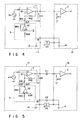
- FIG. 4 shows an embodiment of the present invention using a non-inverting type amplifier as an analog amplifier.
- the signal eil is supplied to a non-inverting input terminal of an operational amplifier 41.
- An output terminal of the operational amplifier 41 is connected to the input terminal of the analog amplifier 2 of the second circuit system 12.
- One end of a resistor R41 is connected to the non-inverting input terminal of the operational amplifier 41 and one end of a resistor R42.
- the other end of the resistor R42 is connected to the output terminal of the operational amplifier 41.
- the reference potential 14 of the second circuit system 12 is supplied to the input terminal IN of the canceling circuit 3.
- the input terminal IN of the canceling circuit 3 is connected to one end of a resistor R43, and the other end of the resistor R43 is connected to the inverting input terminal of the operational amplifier 42.
- the output terminal of the operational amplifier 42 is connected to one end of a resistor R44, and the other end of the resistor R44 is connected to the inverting input terminal of the operational amplifier 42.
- a non-inverting input terminal of the operational amplifier 42 is connected to the reference potential 13 of the first circuit system 11.
- the output terminal of the operational amplifier 42 that is, the output terminal OUT of the canceling circuit 3 is connected to the other end of the resistor R41.
- the operational amplifier 42 serves as a buffer amplifier for supplying an output of Vx times (-R44/R43) at a low impedance to the output terminal OUT of the reference potential difference canceling circuit 3.
- the signal can be received and transmitted between the different circuit systems without generating the noise component.
- the amplifier for generating a differential signal and the amplifier for receiving the differential signal are not needed, so that the manufacturing cost and the circuit occupying area can be reduced.
- FIG. 5 is an embodiment of the present invention showing a case in which the circuit of FIG. 4 is ]operated by a single power supply.
- a non-inverting type amplifier is used as the analog amplifier 1.
- the signal eil is supplied to a non-inverting input terminal of an operational amplifier 51.
- a inverting input terminal of the operational amplifier 51 is connected to one end of the resistor R41, and the other end of the resistor R41 is connected to the output terminal OUT of the canceling circuit 3.
- the inverting input terminal of the operational amplifier 51 is connected to one end of the resistor R42, and the other end of the resistor R42 is connected to the output terminal of the operational amplifier 51.
- the output terminal of the operational amplifier 51 is connected to the input terminal of the analog amplifier 2 of the second circuit system through the coupling condenser C1.
- the input terminal IN of the canceling circuit 3 is connected to the reference potential 14 of the second circuit system through the coupling condenser C2.
- the input terminal IN of the canceling circuit 3 is connected to one end of the resistor R43, and the other end of the resistor R43 is connected to the inverting input terminal of an operational amplifier 52.
- the inverting input terminal of the operational amplifier 52 is connected to one end of the resistor R44, and the other end of the resistor R44 is connected to the output terminal of the operational amplifier 52.
- a non-inverting input terminal of the operational amplifier 52 is connected to another reference potential Vref having a constant potential difference to the reference potential 13 of the first circuit system.
- the reference potential Vref is supplied from a voltage divider using the power supply potential VDD and the reference potential 13 or using the constant power supply.
- the canceling circuit 3 is also used as Vref generator.
- the signal can be received and transmitted between the different circuit systems without generating the noise component.
- the amplifier for generating a differential signal and the amplifier for receiving the differential signal are not needed, so that the manufacturing cost and the circuit occupying area can be reduced.
- the reference potential difference canceling circuit is also used as the Vref generator in operating the amplifier by the single power supply. As a result, increase in the number of parts can be prevented.
- FIG. 6 is an embodiment showing a case of using a differential amplifier as the analog amplifier 1.
- the signal ei- is supplied to one end of a resistor R61, and the other end of the resistor R61 is connected to an inverting input terminal of an operational amplifier 61.
- the inverting input terminal of the operational amplifier 61 is connected to one end of a resistor R62, and the other end of the resistor R62 is connected to the output of the operational amplifier 61.
- the signal ei+ is supplied to one end of a resistor R63, and the other end of the resistor R63 is connected to the non-inverting input terminal of the operational amplifier 61.
- the output terminal of the operational amplifier 61 is connected to the input terminal of the analog amplifier 2 of the second circuit system 12.
- the reference potential 14 of the second circuit system is supplied to the input terminal IN of the canceling circuit 3 of the first circuit system 11.
- the canceling circuit 3 comprises a resistor R64, and R65. One end of the resistor R64 is connected to the input terminal IN of the canceling circuit 3, and the other end of the resistor R64 is connected to the output terminal OUT of the canceling circuit 3. One end of a resistor R65 is connected to the other end of the resistor R64, and the reference potential 13 of the first circuit system is supplied to the other end of the resistor R65.
- the output terminal OUT of the canceling circuit 3 is connected to the non-inverting input terminal of the operational amplifier 61.
- R63'/(R63' + R64) R61/(R61 + R62) may be established.
- the signal can be received and transmitted between the different circuit systems without generating the noise component.
- the amplifier for generating a differential signal and the amplifier for receiving the differential signal are not needed, so that the manufacturing cost and the circuit occupying area can be reduced.
- FIG. 7 is an embodiment showing a case in which the circuit of FIG. 6 is operated by a single power supply.
- the differential analog amplifier 1 is the same as the differential analog amplifier of FIG. 6.
- An output terminal of an operational amplifier 71 is connected to the input terminal of the analog amplifier 2 of the second circuit 12 of the second circuit system 12 through the coupling condenser C1.
- the reference potential 14 of the second circuit system is supplied to the input terminal IN of the canceling circuit 3 through the coupling condenser C2.
- the canceling circuit 3 comprises resistors R64, R65, and R66. Power potential VDD of the first circuit system is supplied to one end of the resistor R66, and the other end of the resistor R66 is connected to the output terminal OUT of the canceling circuit 3. One end of the resistor R65 is connected to the other end of the resistor R66, and the reference potential 13 of the first circuit system 1 is supplied to the other end of the resistor R65. One end of the resistor R64 is connected to the input terminal IN of the canceling circuit 3, and the other end of the resistor R64 is connected to the connection point between the resistors R65 and R66. The output terminal OUT of the canceling circuit 3 is connected to a non-inverting input terminal of an operational amplifier 71.
- the resistor R65 of FIG. 6 is replaced with R65 ⁇ R66/(R65 + R66), so that the resistance condition for canceling Vx can be obtained. Similar to the embodiments of FIGS. 3 and 5, the canceling circuit 3 of this embodiment is also used as a Vref generator.
- the signal can be received and transmitted between the different circuit systems without generating the noise component.
- the amplifier for generating a differential signal and the amplifier for receiving the differential signal are not needed, so that the manufacturing cost and the circuit occupying area can be reduced.
- the reference potential difference canceling circuit is also used as the Vref generator in operating the amplifier by the single power supply. As a result, increase in the number of parts can be prevented.
- FIG. 8 is an embodiment showing a case in which a line for connecting the input terminal IN of the canceling circuit 3 to the second reference potential of the second circuit system is shared when the circuit shown in FIG. 3 is provided for two channels.
- analog amplifiers 1a and 1b and canceling circuits 3a and 3b which are similar to those shown in FIG. 3, are provided in the first circuit system 11.
- the output signals of the analog amplifiers 1a and 1b are supplied to the input analog amplifiers 2a and 2b of the second circuit system 12 through coupling condensers C1a and C1b, respectively.
- the input terminals IN of the canceling circuits 3a and 3b are connected to the reference potential 14 of the second circuit system 12 through a common coupling condenser C2.
- the signal can be received and transmitted between the different circuit systems without generating the noise component.
- the number of condenser C2 for cutting the DC component can be one, so that the number of signals lines and the number of parts of the circuit can be reduced.
- the input signal line for the canceling circuit can be shared.
- FIG. 8 shows the case of the single power supply. However, even in the case of two power supplies as shown in FIG. 2, the connection line between the canceling circuit and the reference potential of the second circuit system can be shared.
- FIG. 9 is an embodiment of the present invention showing a case in which an input signal line of the canceling circuit 3 is shared when the circuit shown in FIG. 5 is provided for two channels.
- two analog amplifiers 1a and 1b which are the same as described in FIG. 5, and two reference potential difference canceling circuits 3a and 3b, which are the same as described in FIG. 5, are provided.
- the output signals of analog amplifiers la and 1b are supplied to input amplifiers 2a and 2b of the second circuit system through coupling condenser C1a and C1b, respectively.
- the input terminal IN of each of the canceling circuits 3a and 3b is connected to the reference potential 14 of the second circuit system through the common condenser C2.
- the signal can be received and transmitted between the different circuit systems without generating the noise component. Similar to the embodiment of FIG. 8, the increase in the number of signal lines and the number of parts can be prevented.
- the input signal line of the canceling circuit 3 can be used as a common input signal line.
- connection line between the input terminal of the canceling circuit 3 and the reference potential of the second circuit system can be used as a common connection line.
- FIG. 10 shows an embodiment in which the reference potential difference canceling circuit 3 is used as a common circuit when the circuit shown in FIG. 3 is provided for two channels.
- one canceling circuit 3 which is the same as shown in FIG. 3, and two inverting type analog amplifiers 1a and 1b, which are the same as shown in FIG. 3, are provided.
- the output signals of the analog amplifiers 1a and 1b are supplied to the input amplifiers 2a and 2b of the second circuit system through the coupling condensers C1a and C1b, respectively.
- the input terminal IN of the canceling circuit 3 is connected to the reference potential 14 of the second circuit system through the coupling condenser C2.
- the output terminal OUT of the canceling circuit 3 is connected to the non-inverting input terminal of the operational amplifier 21a of the analog amplifier la and the non-inverting input terminal of the operational amplifier 21b of the analog amplifier 1b.
- the signal can be received and transmitted between the different circuit systems without generating the noise component.
- the number of parts can be more reduced than the embodiment of FIG. 8.
- the canceling circuit 3 can be used as a common circuit.
- FIG. 10 showed the case of the single power supply. However, even in the case of two power supplies as shown in FIG. 2, the canceling circuit 3 can be used as a common circuit.
- FIG. 11 shows an embodiment of the present invention in which the reference potential difference canceling circuit 3 is used as a common circuit when the circuit shown in FIG. 5 is provided for two channels.
- one canceling circuit 3 which is the same as shown in FIG. 5, and two inverting type analog amplifiers 1a and 1b, which are the same as shown in FIG. 5, are provided.
- the output signals of the analog amplifiers 1a and 1b are supplied to the input amplifiers 2a and 2b of the second circuit system 12 through the coupling condensers C1a and C1b, respectively.
- the input terminal IN of the canceling circuit 3 is connected to the second reference potential of the second circuit system through the coupling condenser C2.
- the output terminal OUT of the canceling circuit 3 is connected to each of the inverting input terminals of operational amplifiers 51a and 51b through each of resistors R41a and R41b.
- the signal can be received and transmitted between the different circuit systems without generating the noise component.
- the number of parts can be more reduced than the embodiment of FIG. 9.
- the canceling circuit 3 can be used as a common circuit.
- FIG. 11 showed the case of the single power supply. However, even in the case of two power supplies as shown in FIG. 4, the canceling circuit 3 can be used as a common circuit.
- FIG. 12 shows an analog amplifier using a switched capacitor.
- the switched capacitor comprises a capacitor C, a switch SWa and a switch SWb.
- the switch SWa has a movable contact, which is connected to the first terminal of the capacitor C, and a fixed contact, which is connected to a terminal a and the reference potential.
- the switch SWb has a movable contact, which is connected to the second terminal of the capacitor C, and a fixed contact, which is connected to a terminal b and the reference potential.
- T shows a period of the opening and closing of each of SWa and SWb.
Description
- The present invention relates to an amplifier for canceling noise generated between circuit systems, and particularly to an analog amplifier, which is applied to, for example, an audio circuit, for preventing noise from being generated to an analog output signal to be sent to the other systems having a different reference potential based on a difference between two circuit systems in the reference potential.
- In recent years, an electronic circuit system has become increasingly complicated. In many cases, the circuit is formed on a plurality of circuit boards, and these plurality of circuit systems are connected by a connection line. In the case of connecting the reference potentials, e.g., ground potentials, of different circuit systems, by the connection line, there occurs a case in which a current flows between the reference potentials or a case in which the connection line acts as an antenna to cause noise to be carried on the connection line. As a result, in many cases, a potential difference occurs between the reference potentials of the different circuit systems. The potential difference generally includes an unfavorable noise component. As a result, particularly, the analog circuit is largely damaged.
- Moreover, in accordance with the circuit digitalization, there is frequently used a system in which the analog circuit and the digital circuit are mixed. In the digital circuit, since a signal receiving and transmitting is carried out by a pulse having large amplitude of 3 to 5V, large nose is generated. In this case, since noise, which is generated between the reference potentials, becomes extremely large, the performance of the analog circuit may extremely deteriorated. Therefore, it is very important to prevent the analog section from being unfavorably influenced by such noise.
- FIG. 15 shows a mechanism in which noise is generated between reference potentials of two circuit systems each formed on a different circuit boards, that is, ground potentials. Arrows illustrated between two
circuit systems first circuit system 111 to thesecond signal system 112 and that the total amount of current 12 flows in transmitting a signal from thesecond circuit system 112 to thefirst circuit system 111. As a result, the current of I1 - I2 flows into a connection line betweenreference potentials first circuit system 111 to thesecond circuit system 112. If the connection line serves as an antenna, a current In, which is generated by noise to enter in a form of a radio wave, also flows into the connection line between the reference potentials. If the connection line between the reference potentials has impedance Z, a reference potential difference Vx between two circuit systems can be expressed by the following equation:
- In this equation, currents I1 and I2 are surely generated in receiving and transmitting the signal. The current I1 and I2 are increased as the system is enlarged and the number of digital circuits is increased. The current In is also increased as the number of the digital circuits is increased, unnecessary amount of radiation is increased and the reference potential connection line becomes long. Moreover, impedance Z is also increased as the connection line between the reference potentials becomes long. Therefore, it can be considered that the reference potential difference Vx becomes large as the scale of the system and the digital section of the system become large.
- The DC component of the reference potential difference Vx can be cut by a coupling condenser. However, the AC component is superimposed on the signal component in receiving and transmitting the analog signal. As a result, transmission property is deteriorated.
- In order to solve such a problem, a signal receiving and transmitting circuit of a differential output type is conventionally used. FIG. 14 shows one example of such a signal receiving and transmitting circuit. This type of the signal receiving and transmitting circuit comprises an amplifier, a
differential amplifier 104, and two signal lines.' The amplifier is provided at an output stage of thefirst circuit system 111 of the signal output side. The amplifier comprises inverting typeanalog amplifiers differential amplifier 104 is provided at an input stage of thesecond circuit system 112 of the signal input side. The differential signals eo+ and eo- are input to thedifferential amplifier 104. Two signal lines transmit the differential signals. This type of the circuit transmits the signal in the form of a differential signal, and receives the signal in the form of a differential signal. As a result, the noise component, which is generated since the reference potentials are not common, is canceled. More specifically, in FIG. 14, it is assumed that the following equations are set:
R102/R101 = 1, R104/R103 = R106/R105 = A - As a result, the potentials eo+ and eo- of the first circuit system, which are seen from the
reference potential 113 of the first circuit system, can be obtained as follows:
- The potentials eo+ and eo-, which are seen from the
differential amplifier 104 of thesecond circuit system 112, are based on thereference potential 114 of the second circuit system, and these potentials can be obtained as follows:
- If the gain of the differential amplifier. 104 of the second circuit system is A', an output potential eo2 of the
differential amplifier 104 can be obtained as follows.
- Thus, noise Vx can be prevented from appearing in the output potential eo2.
- However, in the conventional circuit, three output amplifiers and two signal lines are needed in the transmitter side and the differential input amplifier is needed in the receiver side. As a result, the manufacturing cost and the circuit occupying area are increased.
- EP-0 482 291 discloses an isolator circuit for an audio system having an operational amplifier provided between a signal source and an amplifier. A capacitor and a resistor connected in series are connected between each input of the operational amplifier and the signal source. A buffer amplifier is provided between the capacitor and the resistor of each input line of the operational amplifier.
- An object of the present invention is to provide a circuit for receiving and transmitting a signal without an increasing manufacturing cost and a circuit occupying area and generating a noise component.
- The object can be achieved by the following structure.
- There is provided an amplifier according to the appended
claims - This invention can be more fully understood from the following detailed description when taken in conjunction with the accompanying drawings, in which:
- FIG. 1 is a view showing an embodiment of the present invention;
- FIG. 2 is a view showing an inverting type amplifier of the prior art;
- FIG. 3 is a view showing an inverting type amplifier of a single power supply of the prior art;
- FIG. 4 is a view showing an embodiment of the present invention using a non-inverting type amplifier;
- FIG. 5 is a view showing another embodiment of the present invention using a non-inverting type amplifier;
- FIG. 6 is a view showing a differential amplifier of the prior art;
- FIG. 7 is a view showing a differential amplifier of a single power supply of the prior art;
- FIG. 8 .is a view showing an inverting type amplifier and an input line for a reference potential difference canceling circuit in common of the prior art;
- FIG. 9 is a view showing an embodiment of the present invention using a non-inverting type amplifier and an input line for a reference potential difference canceling circuit in common;
- FIG. 10 is a view showing an inverting type amplifier and a reference potential difference canceling circuit in common of the prior art;
- FIG. 11 is a view showing an embodiment of the present invention using a non-inverting type amplifier and a reference potential difference canceling circuit in common;
- FIG. 12 is a view showing a switched capacitor in an inverting type amplifier of the prior art;
- FIG. 13 is a view showing the relationship between the switched capacitor and resistance;
- FIG. 14 is a view showing a prior art; and
- FIG. 15 is a view showing a mechanism for generating the reference potential difference between two circuit systems.
- The following will explain the embodiments of the present invention with reference to the drawings.
- FIG. 1 shows an embodiment of the present invention. In the following explanation, the same reference numerals are added to the structural elements in common to each other, and the specific explanation will be omitted.
- In the embodiment shown in FIG. 1, each of first and
second circuit systems first circuit system 11 is different from that of thesecond circuit system 12. An analog signal is transmitted from thefirst circuit system 11 to thesecond circuit system 12. - A
reference potential 13 of thefirst circuit system 11 and areference potential 14 of thesecond circuit system 12 are normally set to a ground potential. In FIG. 1, these reference potentials are shown by a different ground potential mark. These two systems are electrically connected to each other through impedance Z formed between thereference potentials - In the
first circuit system 11, a signal eil is supplied to an input terminal of ananalog amplifier 1 whose gain is A. An output signal of theanalog amplifier 1 is transmitted to thesecond circuit system 12 to be supplied to an input terminal of ananalog amplifier 2. If there is no reference potentialdifference canceling circuit 3, an input signal of theanalog amplifier 2 of the second circuit system becomes A x eil + Vx by providing that the reference potential of the second circuit system is set as a reference. As a result, the difference Vx between thereference potentials second circuit system 12. Then, the reference potentialdifference canceling circuit 3 whose gain is 1/A is provided in thefirst circuit system 11. An input terminal of thecircuit 3 is connected to aground point 14, which is the reference potential of thesecond circuit system 12. Then, an output signal of thecircuit 3 is supplied to the input terminal of theanalog amplifier 1 with the signal eil. - In this case, the
reference potential 13 of the first circuit system is set as a reference, so an output signal eol of theanalog amplifier 1 becomes as follows:
- The
reference potential 14 of the second circuit system is set as a reference, so an input signal ei2 of theanalog amplifier 2 becomes as follows:
- In this way, noise component Vx can be removed.
- According to the above-mentioned embodiment, one analog amplifier and the simple reference potential difference canceling circuit are used, so that the signal can be received and transmitted between the different circuit systems without generating the noise component. As a result, it is unnecessary to provide an amplifier for generating a differential signal and an amplifier for receiving the differential signal. Thereby, the manufacturing cost and the circuit occupying area can be reduced.
- FIG. 2 shows an inverting type amplifier as the
analog amplifier 1 shown in FIG. 1. - In the
first circuit system 11, the signal eil is supplied to one end of a resistor R1, and the other end of the resistor R1 is connected to an inverting input terminal of anoperational amplifier 21. The inverting input terminal of theoperational amplifier 21 is connected to one end of a resistor R2, and the other end of the resistor R2 is connected to an output terminal of theoperational amplifier 21. The output terminal of theoperational amplifier 21 is connected to an input terminal of theanalog amplifier 2 of the second circuit system. Thereference potential 14 of thesecond circuit system 12 is supplied to the input terminal IN of the cancelingcircuit 3 of thefirst circuit system 11. The cancelingcircuit 3 is a potential divider using the resistor. In the cancelingcircuit 3, a resistor R3 is provided between the input terminal IN and the output terminal OUT. A resistor R4 is provided between the output terminal OUT and thereference potential 13 of the first circuit system. The output terminal OUT of the cancelingcircuit 3 is connected to a non-inverting input terminal of theoperational amplifier 21. - In this embodiment, gain A- of the
analog amplifier 1, which is seen from the inverting input signal of theoperational amplifier 1, that is, one end of the resistor R1, is as follows:
- Moreover, gain A+ of the
analog amplifier 1, which is seen from the non-inverting input signal of theanalog amplifier 1, that is, the non-inverting input terminal of theoperational amplifier 21, is as follows:
- Therefore, in the canceling
circuit 3, it is assumed that the following equation is given:
i.e: R4/R3 = R1/R2 - As a result, the gain, which is from the input terminal IN of the canceling
circuit 3 to the output terminal of theanalog amplifier 1, becomes 1. In this case, thereference potential 13 of the first circuit system is set as a reference, so the output potential eol of theanalog amplifier 1 becomes as follows:
- Therefore, the
reference potential 14 of the second circuit system is set as a reference, so the input potential ei2 of theanalog amplifier 2 becomes as follows:
- In this way, noise Vx can be canceled.
- According to the above-mentioned embodiment, one analog amplifier and the simple reference potential difference canceling circuit are used, so that the signal can be received and transmitted between the different circuit systems without generating the noise component. As a result, it is unnecessary to provide an amplifier for generating a differential signal and an amplifier for receiving the differential signal. Thereby, the manufacturing cost and the circuit occupying area can be reduced.
- FIG. 3 shows an inverting input type amplifier as the
analog amplifier 1 of a single power supply. - The
analog amplifier 1 of this embodiment comprises anoperational amplifier 21, and resistors R1 and R2, and is the same as the analog amplifier of FIG. 2. The signal eil is supplied to one end of the resistor R1, and the other end of the resistor R1 is connected to an inverting input terminal of theoperational amplifier 21. An output terminal of theoperational amplifier 21 is connected to the input terminal of theanalog amplifier 2 of the second circuit system through a coupling condenser C1. - The
reference potential 14 of thesecond circuit system 12 is supplied to the input terminal IN of the cancelingcircuit 3 of thefirst circuit system 11 through a coupling condenser C2. - In the canceling
circuit 3, a resistor R15 is provided between the input terminal IN and the output terminal OUT. A resistor R13 is provided between a power supply potential VDD of the first circuit system and the output terminal OUT. A resistor R14 is provided between the output terminal OUT and the reference potential of the first circuit system. The output terminal OUT of the cancelingcircuit 3 is connected to the non-inverting input terminal of theoperational amplifier 21. - In the embodiment shown in FIG. 2, since the input signal eil of the
analog amplifier 1 swings around a ground potential, positive and negative power-supply sources are needed as a power supply for theanalog amplifier 1. In the case of using the single power supply, the input signal eil cannot swing around the ground potential. Due to this, another reference potential Vref must be provided. The reference potential Vref is normally set to a half of the power supply potential. In this case, the input signal eil of theanalog amplifier 1 becomes as follows:
In this case, es is an input signal, which does not include a DC component. As a result, the input signal eil swings around the reference potential Vref. The cancelingcircuit 3 shown in FIG. 3 is also used as a Vref generator. The reference potential Vref is a DC value. The Reference potential Vref is provided on a common junction of the resistors R13 and R14 by dividing the potential between the power supply potential VDD and thereference potential 13. In a case where the power supply potential VDD is unstable, there can be considered a method in which a stable potential is created and the reference potential Vref is provided by dividing the potential between the stable potential and thereference potential 13. - Unlike the embodiment shown in FIG. 2, the input terminal IN of the canceling
circuit 3 shown in FIG. 3 is connected to thereference potential 14 of the second circuit system through the coupling condenser C2. Due to this, only AC component of noise Vx is input to the cancelingcircuit 3. In other words, DC component of noise Vx cannot be canceled. However, in the case of the single power supply, the output terminal of theanalog amplifier 1 and the input terminal of theanalog amplifier 2 are connected to each other through the coupling condenser C1. In this case, since the DC component does not pass through the coupling condenser C1, it is unnecessary to cancel the DC component. The gain of the cancelingcircuit 3 against the AC component can be obtained by replacing the resistor R4 in FIG. 2 with the parallel connection of resistors R13 and R14. If the resistance value of the parallel connection is set to R4', the following equation can be established:
- To cancel noise, the following equation may be established:

- Therefore, if the following equation is established, the AC component of noise Vx can be canceled similar to the case of FIG. 2.

- According to the above-mentioned embodiment, one analog amplifier and the simple reference potential difference canceling circuit are used, so that the signal can be received and transmitted between the different circuit systems without generating the noise component. As a result, it is unnecessary to provide an amplifier for generating a differential signal and an amplifier for receiving the differential signal. Thereby, the manufacturing cost and the circuit occupying area can be reduced.
- Moreover, according to the above-mentioned embodiment, since the reference potential difference canceling circuit is also used as the Vref generator in operating the amplifier by the single power supply. As a result, increase in the number of parts can be prevented.
- FIG. 4 shows an embodiment of the present invention using a non-inverting type amplifier as an analog amplifier.
- The signal eil is supplied to a non-inverting input terminal of an
operational amplifier 41. An output terminal of theoperational amplifier 41 is connected to the input terminal of theanalog amplifier 2 of thesecond circuit system 12. One end of a resistor R41 is connected to the non-inverting input terminal of theoperational amplifier 41 and one end of a resistor R42. The other end of the resistor R42 is connected to the output terminal of theoperational amplifier 41. - The
reference potential 14 of thesecond circuit system 12 is supplied to the input terminal IN of the cancelingcircuit 3. In the cancelingcircuit 3, the input terminal IN of the cancelingcircuit 3 is connected to one end of a resistor R43, and the other end of the resistor R43 is connected to the inverting input terminal of theoperational amplifier 42. Also, the output terminal of theoperational amplifier 42 is connected to one end of a resistor R44, and the other end of the resistor R44 is connected to the inverting input terminal of theoperational amplifier 42. A non-inverting input terminal of theoperational amplifier 42 is connected to thereference potential 13 of thefirst circuit system 11. The output terminal of theoperational amplifier 42, that is, the output terminal OUT of the cancelingcircuit 3 is connected to the other end of the resistor R41. Theoperational amplifier 42 serves as a buffer amplifier for supplying an output of Vx times (-R44/R43) at a low impedance to the output terminal OUT of the reference potentialdifference canceling circuit 3. - Then, gain A- of the
analog amplifier 1 seen from the inverting input signal of theanalog amplifier 1, that is, the other end of the resistor R41 can be given as follows:
- Therefore, if the following equation is given,
R44/R43 = R41/R42
the gain, which is from input terminal IN of the cancelingcircuit 3 to the output terminal of theamplifier 1, becomes 1. As a result, the following equation can be established.
- Then, it is possible to prevent noise Vx from appearing in the input signal ei2 of the
analog amplifier 2. - According to the above-explained embodiment, by use of one analog amplifier and the simple reference potential difference canceling circuit, the signal can be received and transmitted between the different circuit systems without generating the noise component. As a result, the amplifier for generating a differential signal and the amplifier for receiving the differential signal are not needed, so that the manufacturing cost and the circuit occupying area can be reduced.
- FIG. 5 is an embodiment of the present invention showing a case in which the circuit of FIG. 4 is ]operated by a single power supply.
- In the embodiment of FIG. 5, a non-inverting type amplifier is used as the
analog amplifier 1. The signal eil is supplied to a non-inverting input terminal of anoperational amplifier 51. A inverting input terminal of theoperational amplifier 51 is connected to one end of the resistor R41, and the other end of the resistor R41 is connected to the output terminal OUT of the cancelingcircuit 3. Also, the inverting input terminal of theoperational amplifier 51 is connected to one end of the resistor R42, and the other end of the resistor R42 is connected to the output terminal of theoperational amplifier 51. The output terminal of theoperational amplifier 51 is connected to the input terminal of theanalog amplifier 2 of the second circuit system through the coupling condenser C1.
The input terminal IN of the cancelingcircuit 3 is connected to thereference potential 14 of the second circuit system through the coupling condenser C2. - In the canceling
circuit 3, the input terminal IN of the cancelingcircuit 3 is connected to one end of the resistor R43, and the other end of the resistor R43 is connected to the inverting input terminal of anoperational amplifier 52. The inverting input terminal of theoperational amplifier 52 is connected to one end of the resistor R44, and the other end of the resistor R44 is connected to the output terminal of theoperational amplifier 52. A non-inverting input terminal of theoperational amplifier 52 is connected to another reference potential Vref having a constant potential difference to thereference potential 13 of the first circuit system. As mentioned in the explanation of FIG. 3, the reference potential Vref is supplied from a voltage divider using the power supply potential VDD and thereference potential 13 or using the constant power supply. - In this embodiment, AC component of Vx can be canceled by satisfying the equation shown in the embodiment of FIG. 4. Specifically, if R44/R43 = R41/R42 is established, the gain, which is from the input terminal IN of the canceling
circuit 3 to the output terminal of theanalog amplifier 1, becomes 1. As a result, noise of the input signal of theanalog amplifier 2 can be canceled. In this embodiment, similar to the embodiment of FIG. 3, the cancelingcircuit 3 is also used as Vref generator. - Thus, according to the above-explained embodiment, by use of one analog amplifier and the simple reference potential difference canceling circuit, the signal can be received and transmitted between the different circuit systems without generating the noise component. As a result, the amplifier for generating a differential signal and the amplifier for receiving the differential signal are not needed, so that the manufacturing cost and the circuit occupying area can be reduced.
- Moreover, according to the above-mentioned embodiment, since the reference potential difference canceling circuit is also used as the Vref generator in operating the amplifier by the single power supply. As a result, increase in the number of parts can be prevented.
- FIG. 6 is an embodiment showing a case of using a differential amplifier as the
analog amplifier 1. - In this embodiment, the signal ei- is supplied to one end of a resistor R61, and the other end of the resistor R61 is connected to an inverting input terminal of an
operational amplifier 61. The inverting input terminal of theoperational amplifier 61 is connected to one end of a resistor R62, and the other end of the resistor R62 is connected to the output of theoperational amplifier 61. The signal ei+ is supplied to one end of a resistor R63, and the other end of the resistor R63 is connected to the non-inverting input terminal of theoperational amplifier 61. The output terminal of theoperational amplifier 61 is connected to the input terminal of theanalog amplifier 2 of thesecond circuit system 12. - The
reference potential 14 of the second circuit system is supplied to the input terminal IN of the cancelingcircuit 3 of thefirst circuit system 11. The cancelingcircuit 3 comprises a resistor R64, and R65. One end of the resistor R64 is connected to the input terminal IN of the cancelingcircuit 3, and the other end of the resistor R64 is connected to the output terminal OUT of the cancelingcircuit 3. One end of a resistor R65 is connected to the other end of the resistor R64, and thereference potential 13 of the first circuit system is supplied to the other end of the resistor R65. The output terminal OUT of the cancelingcircuit 3 is connected to the non-inverting input terminal of theoperational amplifier 61. - In this embodiment, the output signal eol of the
analog amplifier 1 can be expressed as follows:
where, R64' = R64 × R65/(R64 + R65) - Similar to the case shown in FIG. 2, the gain A+ of the
analog amplifier 1 seen from the non-inverting input terminal can be expressed as follows:
- Moreover, the gain A', which is from the input terminal IN of the canceling
circuit 3 to the output terminal OUT, can be expressed as follows:
where, R63' = R63 × R65/(R63 + R65) - If the equation, A' = 1/(A+), is established, Vx can be canceled.
- Therefore, R63'/(R63' + R64) = R61/(R61 + R62) may be established.
- Then, if the following equation is given, Vx can be canceled.
R63'/R64 = R61/R62

- Thus, according to the above-explained embodiment, by use of one analog amplifier and the simple reference potential difference canceling circuit, the signal can be received and transmitted between the different circuit systems without generating the noise component. As a result, the amplifier for generating a differential signal and the amplifier for receiving the differential signal are not needed, so that the manufacturing cost and the circuit occupying area can be reduced.
- FIG. 7 is an embodiment showing a case in which the circuit of FIG. 6 is operated by a single power supply.
- In the embodiment of FIG. 7, the
differential analog amplifier 1 is the same as the differential analog amplifier of FIG. 6. An output terminal of anoperational amplifier 71 is connected to the input terminal of theanalog amplifier 2 of thesecond circuit 12 of thesecond circuit system 12 through the coupling condenser C1. Thereference potential 14 of the second circuit system is supplied to the input terminal IN of the cancelingcircuit 3 through the coupling condenser C2. - The canceling
circuit 3 comprises resistors R64, R65, and R66. Power potential VDD of the first circuit system is supplied to one end of the resistor R66, and the other end of the resistor R66 is connected to the output terminal OUT of the cancelingcircuit 3. One end of the resistor R65 is connected to the other end of the resistor R66, and thereference potential 13 of thefirst circuit system 1 is supplied to the other end of the resistor R65. One end of the resistor R64 is connected to the input terminal IN of the cancelingcircuit 3, and the other end of the resistor R64 is connected to the connection point between the resistors R65 and R66. The output terminal OUT of the cancelingcircuit 3 is connected to a non-inverting input terminal of anoperational amplifier 71. - In this embodiment, the resistor R65 of FIG. 6 is replaced with R65 × R66/(R65 + R66), so that the resistance condition for canceling Vx can be obtained. Similar to the embodiments of FIGS. 3 and 5, the canceling
circuit 3 of this embodiment is also used as a Vref generator. - Thus, according to the above-explained embodiment, by use of one analog amplifier and the simple reference potential difference canceling circuit, the signal can be received and transmitted between the different circuit systems without generating the noise component. As a result, the amplifier for generating a differential signal and the amplifier for receiving the differential signal are not needed, so that the manufacturing cost and the circuit occupying area can be reduced.
- Moreover, according to the above-mentioned embodiment, since the reference potential difference canceling circuit is also used as the Vref generator in operating the amplifier by the single power supply. As a result, increase in the number of parts can be prevented.
- FIG. 8 is an embodiment showing a case in which a line for connecting the input terminal IN of the canceling
circuit 3 to the second reference potential of the second circuit system is shared when the circuit shown in FIG. 3 is provided for two channels. - In this embodiment,
analog amplifiers 1a and 1b and cancelingcircuits 3a and 3b, which are similar to those shown in FIG. 3, are provided in thefirst circuit system 11. The output signals of theanalog amplifiers 1a and 1b are supplied to theinput analog amplifiers 2a and 2b of thesecond circuit system 12 through coupling condensers C1a and C1b, respectively. The input terminals IN of the cancelingcircuits 3a and 3b are connected to thereference potential 14 of thesecond circuit system 12 through a common coupling condenser C2. - Thus, according to this embodiment, the signal can be received and transmitted between the different circuit systems without generating the noise component. Moreover, the number of condenser C2 for cutting the DC component can be one, so that the number of signals lines and the number of parts of the circuit can be reduced.
- Similarly, in a case where three or more channels are provided in the circuit, the input signal line for the canceling circuit can be shared.
- The embodiment of FIG. 8 shows the case of the single power supply. However, even in the case of two power supplies as shown in FIG. 2, the connection line between the canceling circuit and the reference potential of the second circuit system can be shared.
- FIG. 9 is an embodiment of the present invention showing a case in which an input signal line of the canceling
circuit 3 is shared when the circuit shown in FIG. 5 is provided for two channels. - In this embodiment, in the first circuit system, two
analog amplifiers 1a and 1b, which are the same as described in FIG. 5, and two reference potentialdifference canceling circuits 3a and 3b, which are the same as described in FIG. 5, are provided. The output signals of analog amplifiers la and 1b are supplied to inputamplifiers 2a and 2b of the second circuit system through coupling condenser C1a and C1b, respectively. The input terminal IN of each of the cancelingcircuits 3a and 3b is connected to thereference potential 14 of the second circuit system through the common condenser C2. - According to this embodiment, the signal can be received and transmitted between the different circuit systems without generating the noise component. Similar to the embodiment of FIG. 8, the increase in the number of signal lines and the number of parts can be prevented.
- Moreover, in the case of three or more channels, the input signal line of the canceling
circuit 3 can be used as a common input signal line. - The embodiment of FIG. 9 showed the case of the single power source. However, even in the case of two power supplies as shown in FIG. 4, the connection line between the input terminal of the canceling
circuit 3 and the reference potential of the second circuit system can be used as a common connection line. - FIG. 10 shows an embodiment in which the reference potential
difference canceling circuit 3 is used as a common circuit when the circuit shown in FIG. 3 is provided for two channels. - In the
first circuit system 11, one cancelingcircuit 3, which is the same as shown in FIG. 3, and two invertingtype analog amplifiers 1a and 1b, which are the same as shown in FIG. 3, are provided. The output signals of theanalog amplifiers 1a and 1b are supplied to theinput amplifiers 2a and 2b of the second circuit system through the coupling condensers C1a and C1b, respectively. The input terminal IN of the cancelingcircuit 3 is connected to thereference potential 14 of the second circuit system through the coupling condenser C2. The output terminal OUT of the cancelingcircuit 3 is connected to the non-inverting input terminal of the operational amplifier 21a of the analog amplifier la and the non-inverting input terminal of theoperational amplifier 21b of theanalog amplifier 1b. - According to this embodiment, the signal can be received and transmitted between the different circuit systems without generating the noise component. The number of parts can be more reduced than the embodiment of FIG. 8.
- Moreover, in the case of three or more channels, the canceling
circuit 3 can be used as a common circuit. - The embodiment of FIG. 10 showed the case of the single power supply. However, even in the case of two power supplies as shown in FIG. 2, the canceling
circuit 3 can be used as a common circuit. - FIG. 11 shows an embodiment of the present invention in which the reference potential
difference canceling circuit 3 is used as a common circuit when the circuit shown in FIG. 5 is provided for two channels. - In the
first circuit system 11, one cancelingcircuit 3, which is the same as shown in FIG. 5, and two invertingtype analog amplifiers 1a and 1b, which are the same as shown in FIG. 5, are provided. The output signals of theanalog amplifiers 1a and 1b are supplied to theinput amplifiers 2a and 2b of thesecond circuit system 12 through the coupling condensers C1a and C1b, respectively. The input terminal IN of the cancelingcircuit 3 is connected to the second reference potential of the second circuit system through the coupling condenser C2. The output terminal OUT of the cancelingcircuit 3 is connected to each of the inverting input terminals ofoperational amplifiers 51a and 51b through each of resistors R41a and R41b. - According to this embodiment, the signal can be received and transmitted between the different circuit systems without generating the noise component. The number of parts can be more reduced than the embodiment of FIG. 9.
- Even in a case of three or more channels, the canceling
circuit 3 can be used as a common circuit. - The embodiment of FIG. 11 showed the case of the single power supply. However, even in the case of two power supplies as shown in FIG. 4, the canceling
circuit 3 can be used as a common circuit. - FIG. 12 shows an analog amplifier using a switched capacitor.
- In the circuit shown in FIG. 12, the resistors R1 and R2, which are connected to the
operational amplifier 21 of theanalog amplifier 1 shown in FIG. 2, are replaced with the switched capacitor. - As shown in FIG. 13, the switched capacitor comprises a capacitor C, a switch SWa and a switch SWb. The switch SWa has a movable contact, which is connected to the first terminal of the capacitor C, and a fixed contact, which is connected to a terminal a and the reference potential. The switch SWb has a movable contact, which is connected to the second terminal of the capacitor C, and a fixed contact, which is connected to a terminal b and the reference potential. The switched capacitor can be considered to be equivalent to the resistor R of FIG. 13 by the following equation.
T/C = R - In this case, T shows a period of the opening and closing of each of SWa and SWb. This equation can be established when the frequency of the signal is sufficiently low against f = 1/T. SW1, SW2, and C11 of FIG. 12 correspond to R1 of FIG. 2, and SW2, SW3, and C2 correspond to R2 of FIG. 2.
- Even in the circuit using the switched capacitor, the same advantage as in the above embodiments using the resistor can be obtained. Moreover, since the resistor value R can be changed by changing the period T, variations in the manufacture can be controlled.
Claims (7)
- An amplifier comprising:a first circuit system (11) having an analog amplifier (1) for amplifying a transmitting signal (eil) based on a reference potential (13) of the first circuit system;a second circuit system (12) for receiving an output signal of said analog amplifier (1) based on a reference potential (14) of the second circuit system; andand a reference potential difference canceling circuit (3) wherein the reference potential (14) of said second circuit system is supplied to an input terminal (IN) of said reference potential difference cancelling circuit (3), an output signal of said reference potential difference cancelling circuit (3) is supplied to the input terminal of said analog amplifier (1) together with said transmitting signal, and a gain, from the input terminal (IN) of said reference potential difference cancelling circuit (3) to an output terminal of said analog amplifier (1), is 1, andsaid analog amplifier (1) comprises:a first operational amplifier (41) having a non-inverting input terminal to which said transmitting signal (eil) is supplied;a first resistor (R41) having one end connected to the inverting input terminal of said first operational amplifier (41); anda second resistor (R42) having one end connected to the inverting input terminal of said first operational amplifier (41), and the other end connected to an output terminal of said first operational amplifier (41);characterized in that said reference potential difference cancelling circuit (13) comprises:a second operational (42) amplifier having a non-inverting input terminal to which the reference potential (13) of said first circuit system is supplied, and an output terminal connected to the other end of said first resistor (R41);a third resistor (R43) having one end connected to the input terminal (IN) of said reference potential difference cancelling circuit, and the other end connected to the inverting input terminal of said second operational amplifier (42); anda fourth resistor (R44) having one end connected to the inverting input terminal of said second operational amplifier (42), and the other end connected to the output terminal of said second operational amplifier (42).
- An amplifier comprising:a first circuit system (11) having an analog amplifier (1) for amplifying a transmitting signal (eil) based on a reference potential (13) of the first circuit system;a second circuit system (12) for receiving an output signal of said analog amplifier (1) based on a reference potential (14) of the second circuit system; anda reference potential difference cancelling circuit (3) wherein the reference potential (14) of said second circuit system is supplied to an input terminal (IN) of said reference potential difference cancelling circuit (3), an output signal of said reference potential difference cancelling circuit (3) is supplied to the input terminal of said analog amplifier (1) together with said transmitting signal, and a gain, from the input terminal (IN) of said reference potential difference cancelling circuit (3) to an output terminal of said analog amplifier (1), is 1;wherein said analog amplifier (1) comprises:a first operational amplifier (51) having a non-inverting input terminal to which said transmitting signal (eil) is supplied;a first resistor (R41) having one end connected to the inverting input terminal of said first operational amplifier (51); anda second resistor (R42) having one end connected to the inverting input terminal of said first operational amplifier (51), and the other end connected to an output terminal of said first operational amplifier (51);characterized in that said reference potential difference cancelling circuit (3) comprises :a second operational amplifier (52) having a non-inverting input terminal to which a third reference potential (Vref) having a constant potential to the reference potential (13) of said first circuit system is supplied, and an output terminal connected to the other end of said first resistor (R41);a third resistor (R43) having one end connected to an input terminal (IN) of said reference potential difference cancelling circuit, and the other end connected to an inverting input terminal of said second operational amplifier (52); anda fourth resistor (R44) having one end connected to the inverting input terminal of said second operational amplifier (52), and the other end connected to the output terminal of said second operational amplifier (52).
- The amplifier according to claim 1 or 2, characterized in that said reference potential difference cancelling circuit (3) is also used as a reference d.c. potential generator of a single power supply amplifier.
- The amplifier according to claim 2, characterized in that the output terminal of the analog amplifier (1) of said first circuit system and the input terminal of said second circuit system (12) are connected through a coupling condenser (C1); and
the input terminal (IN) of said reference potential difference cancelling circuit and the reference potential (14) of said second circuit system are connected through the coupling condenser (C2). - The amplifier according to claims 1 or 2, characterized in that each of said first and second resistors comprises a switched capacitor.
- The amplifier according to any preceding claims, characterized in that a plurality of said analog amplifiers (1a, 1b) is provided;
said reference potential difference cancelling circuit (3a, 3b) is provided in each of said plurality of said analog amplifiers one by one; and
the input terminal of each of said reference potential difference cancelling circuits is connected to the reference potential of said second circuit system through a common signal line. - The amplifier according to any of claims 1 to 5, characterized in that a plurality of the analog amplifiers (1a, 1b) is provided; and
a common reference potential difference cancelling circuit (3) is provided to each of said plurality of the analog amplifiers.
Applications Claiming Priority (3)
| Application Number | Priority Date | Filing Date | Title |
|---|---|---|---|
| JP12464996 | 1996-05-20 | ||
| JP124649/96 | 1996-05-20 | ||
| JP12464996A JP3410901B2 (en) | 1996-05-20 | 1996-05-20 | Amplifier circuit |
Publications (3)
| Publication Number | Publication Date |
|---|---|
| EP0809353A2 EP0809353A2 (en) | 1997-11-26 |
| EP0809353A3 EP0809353A3 (en) | 1999-07-14 |
| EP0809353B1 true EP0809353B1 (en) | 2006-06-21 |
Family
ID=14890640
Family Applications (1)
| Application Number | Title | Priority Date | Filing Date |
|---|---|---|---|
| EP97107186A Expired - Lifetime EP0809353B1 (en) | 1996-05-20 | 1997-04-30 | Amplifier for cancelling noise between circuit systems |
Country Status (6)
| Country | Link |
|---|---|
| US (1) | US5841308A (en) |
| EP (1) | EP0809353B1 (en) |
| JP (1) | JP3410901B2 (en) |
| KR (1) | KR100253727B1 (en) |
| DE (1) | DE69736153T2 (en) |
| TW (1) | TW350171B (en) |
Families Citing this family (17)
| Publication number | Priority date | Publication date | Assignee | Title |
|---|---|---|---|---|
| US6040728A (en) * | 1998-05-29 | 2000-03-21 | Lucent Technologies, Inc. | Active substrate noise injection cancellation |
| FR2793622B1 (en) * | 1999-05-10 | 2004-03-12 | Peugeot Citroen Automobiles Sa | DEVICE FOR CONNECTING A SOURCE TO AUDIOPHONIC BROADCASTING EQUIPMENT IN PARTICULAR OF A MOTOR VEHICLE |
| US6208190B1 (en) * | 1999-05-27 | 2001-03-27 | Lucent Technologies Inc. | Minimizing effects of switching noise in mixed signal chips |
| JP3666317B2 (en) * | 1999-09-07 | 2005-06-29 | セイコーエプソン株式会社 | Transmission circuit, reception circuit, transmission / reception circuit, and electro-optical device |
| EP1220444A1 (en) * | 2000-12-28 | 2002-07-03 | Alcatel | Differential output amplifier arrangement |
| US7256645B2 (en) * | 2002-11-28 | 2007-08-14 | Nxp B.V. | Suppression of noise in an integrated circuit |
| US6937099B2 (en) * | 2003-12-04 | 2005-08-30 | Analog Devices, Inc. | Op-amp configurable in a non-inverting mode with a closed loop gain greater than one with output voltage correction for a time varying voltage reference of the op-amp, and a method for correcting the output voltage of such an op-amp for a time varying voltage reference |
| US6958642B2 (en) * | 2003-12-19 | 2005-10-25 | Caterpillar Inc | Ground difference compensating system |
| WO2007132297A1 (en) * | 2006-05-16 | 2007-11-22 | Freescale Semiconductor, Inc. | Amplifier circuit and integrated circuit therefor |
| US7391348B2 (en) * | 2006-10-23 | 2008-06-24 | Agere Systems Inc. | Reducing noise associated with local reference-potential fluctuations in mixed-signal integrated circuits |
| US20080309379A1 (en) * | 2007-03-02 | 2008-12-18 | Carroll Sean C | Zero crossing circuit |
| US7944290B2 (en) * | 2009-01-26 | 2011-05-17 | Sumitomo Electric Industries, Ltd. | Trans-impedance amplifier |
| JP5517777B2 (en) | 2010-06-25 | 2014-06-11 | 日立オートモティブシステムズ株式会社 | System having disconnection detection circuit and disconnection detection means for bridge circuit |
| US9151783B2 (en) * | 2012-04-26 | 2015-10-06 | Synopsys, Inc. | Ground offset monitor and compensator |
| JP6027444B2 (en) * | 2013-01-07 | 2016-11-16 | ローム株式会社 | Audio signal processing circuit and in-vehicle audio apparatus, audio component apparatus, and electronic device using the same |
| RU2710395C1 (en) * | 2016-05-16 | 2019-12-26 | ДжейЭкс НИППОН МАЙНИНГ ЭНД МЕТАЛЗ КОРПОРЕЙШН | Method of extracting junior metal and/or rare-earth metal |
| EP3667907B1 (en) | 2018-12-14 | 2022-09-14 | Stichting IMEC Nederland | A read-out circuitry for acquiring a multi-channel biopotential signal and a sensor for sensing a biopotential signal |
Family Cites Families (7)
| Publication number | Priority date | Publication date | Assignee | Title |
|---|---|---|---|---|
| DE2830033A1 (en) * | 1978-07-07 | 1980-01-17 | Hellige Gmbh | AMPLIFIER ARRANGEMENT WITH NOISE REDUCTION |
| JPS59200508A (en) * | 1983-04-26 | 1984-11-13 | Pioneer Electronic Corp | Amplifier |
| JP3167319B2 (en) * | 1990-10-25 | 2001-05-21 | パイオニア株式会社 | Isolator circuit |
| JP2516706B2 (en) * | 1990-11-24 | 1996-07-24 | ローム株式会社 | Amplifier |
| US5648738A (en) * | 1994-11-01 | 1997-07-15 | Cirrus Logic, Inc. | Read channel having auto-zeroing and offset compensation, and power-down between servo fields |
| US5661423A (en) * | 1995-12-14 | 1997-08-26 | Lucent Technologies Inc. | High speed comparator circuits with offset voltage compensation |
| US5606273A (en) * | 1996-03-28 | 1997-02-25 | Caterpillar Inc. | Zero crossing detector circuit |
-
1996
- 1996-05-20 JP JP12464996A patent/JP3410901B2/en not_active Expired - Fee Related
-
1997
- 1997-04-29 US US08/848,269 patent/US5841308A/en not_active Expired - Lifetime
- 1997-04-30 EP EP97107186A patent/EP0809353B1/en not_active Expired - Lifetime
- 1997-04-30 DE DE69736153T patent/DE69736153T2/en not_active Expired - Lifetime
- 1997-05-09 TW TW086106204A patent/TW350171B/en not_active IP Right Cessation
- 1997-05-16 KR KR1019970018859A patent/KR100253727B1/en not_active IP Right Cessation
Also Published As
| Publication number | Publication date |
|---|---|
| KR970078028A (en) | 1997-12-12 |
| JP3410901B2 (en) | 2003-05-26 |
| EP0809353A3 (en) | 1999-07-14 |
| JPH09312525A (en) | 1997-12-02 |
| TW350171B (en) | 1999-01-11 |
| DE69736153T2 (en) | 2007-05-03 |
| EP0809353A2 (en) | 1997-11-26 |
| US5841308A (en) | 1998-11-24 |
| KR100253727B1 (en) | 2000-04-15 |
| DE69736153D1 (en) | 2006-08-03 |
Similar Documents
| Publication | Publication Date | Title |
|---|---|---|
| EP0809353B1 (en) | Amplifier for cancelling noise between circuit systems | |
| EP0151014B1 (en) | Radio transceiver including an antenna switching circuit | |
| JP3189546B2 (en) | Transmitter / receiver circuit | |
| US4571554A (en) | Balanced amplifier device | |
| US5317597A (en) | Resistance coupled data transmission arrangement | |
| EP1098412A3 (en) | Circuit breaker having programmable amplifier | |
| JPH07212257A (en) | Abnormal transmission stop circuit for transmitter | |
| EP0868035A2 (en) | Analog signal transmission circuit | |
| US6426970B1 (en) | Bi-directional signal coupler method and apparatus | |
| KR20020060753A (en) | Means for compensating a data-dependent supply current in an electronic circuit | |
| EP0124315B1 (en) | Amplifiers | |
| WO2002015421A2 (en) | Method and apparatus for transmit digital-to-analog conversion (dac) gain variation compensation | |
| JPH0624327B2 (en) | Terminal device | |
| US20030081663A1 (en) | Interface circuit of differential signaling system | |
| US4554415A (en) | Bilateral amplifier | |
| EP1481488B1 (en) | TRANSMITTER/RECEIVER FOR BIDIRECTIONAL COMMUNICATIONS | |
| JPH08162860A (en) | Offset voltage adjustment circuit | |
| JP3377801B2 (en) | High frequency signal switching circuit | |
| EP0473165A1 (en) | Push-pull power amplifying circuit | |
| GB2050771A (en) | Car-mounted audio equipment | |
| JPS6376529A (en) | Power line carrier transmitter-receiver | |
| JPH0572139B2 (en) | ||
| KR100208208B1 (en) | Input/output separate circuit for half-duplex communication in wireless communication device | |
| JP3288944B2 (en) | Signal transmission system | |
| GB2088665A (en) | Noise suppression system |
Legal Events
| Date | Code | Title | Description |
|---|---|---|---|
| PUAI | Public reference made under article 153(3) epc to a published international application that has entered the european phase |
Free format text: ORIGINAL CODE: 0009012 |
|
| 17P | Request for examination filed |
Effective date: 19970430 |
|
| AK | Designated contracting states |
Kind code of ref document: A2 Designated state(s): DE FR GB |
|
| PUAL | Search report despatched |
Free format text: ORIGINAL CODE: 0009013 |
|
| AK | Designated contracting states |
Kind code of ref document: A3 Designated state(s): DE FR GB |
|
| 17Q | First examination report despatched |
Effective date: 20010326 |
|
| GRAP | Despatch of communication of intention to grant a patent |
Free format text: ORIGINAL CODE: EPIDOSNIGR1 |
|
| GRAS | Grant fee paid |
Free format text: ORIGINAL CODE: EPIDOSNIGR3 |
|
| GRAA | (expected) grant |
Free format text: ORIGINAL CODE: 0009210 |
|
| AK | Designated contracting states |
Kind code of ref document: B1 Designated state(s): DE FR GB |
|
| REG | Reference to a national code |
Ref country code: GB Ref legal event code: FG4D |
|
| REF | Corresponds to: |
Ref document number: 69736153 Country of ref document: DE Date of ref document: 20060803 Kind code of ref document: P |
|
| PLBE | No opposition filed within time limit |
Free format text: ORIGINAL CODE: 0009261 |
|
| STAA | Information on the status of an ep patent application or granted ep patent |
Free format text: STATUS: NO OPPOSITION FILED WITHIN TIME LIMIT |
|
| EN | Fr: translation not filed | ||
| 26N | No opposition filed |
Effective date: 20070322 |
|
| GBPC | Gb: european patent ceased through non-payment of renewal fee |
Effective date: 20070430 |
|
| PG25 | Lapsed in a contracting state [announced via postgrant information from national office to epo] |
Ref country code: GB Free format text: LAPSE BECAUSE OF NON-PAYMENT OF DUE FEES Effective date: 20070430 Ref country code: FR Free format text: LAPSE BECAUSE OF FAILURE TO SUBMIT A TRANSLATION OF THE DESCRIPTION OR TO PAY THE FEE WITHIN THE PRESCRIBED TIME-LIMIT Effective date: 20070309 |
|
| PG25 | Lapsed in a contracting state [announced via postgrant information from national office to epo] |
Ref country code: FR Free format text: LAPSE BECAUSE OF FAILURE TO SUBMIT A TRANSLATION OF THE DESCRIPTION OR TO PAY THE FEE WITHIN THE PRESCRIBED TIME-LIMIT Effective date: 20060621 |
|
| PGFP | Annual fee paid to national office [announced via postgrant information from national office to epo] |
Ref country code: DE Payment date: 20120502 Year of fee payment: 16 |
|
| PG25 | Lapsed in a contracting state [announced via postgrant information from national office to epo] |
Ref country code: DE Free format text: LAPSE BECAUSE OF NON-PAYMENT OF DUE FEES Effective date: 20131101 |
|
| REG | Reference to a national code |
Ref country code: DE Ref legal event code: R119 Ref document number: 69736153 Country of ref document: DE Effective date: 20131101 |