EP0809251A2 - Einchipspeichersystem mit einer gruppierten Bitleitungsstruktur zur simultanen Ausgabe einer Mehrzahl von Daten - Google Patents
Einchipspeichersystem mit einer gruppierten Bitleitungsstruktur zur simultanen Ausgabe einer Mehrzahl von Daten Download PDFInfo
- Publication number
- EP0809251A2 EP0809251A2 EP97103270A EP97103270A EP0809251A2 EP 0809251 A2 EP0809251 A2 EP 0809251A2 EP 97103270 A EP97103270 A EP 97103270A EP 97103270 A EP97103270 A EP 97103270A EP 0809251 A2 EP0809251 A2 EP 0809251A2
- Authority
- EP
- European Patent Office
- Prior art keywords
- reference voltage
- mos transistor
- activation signal
- memory system
- level
- Prior art date
- Legal status (The legal status is an assumption and is not a legal conclusion. Google has not performed a legal analysis and makes no representation as to the accuracy of the status listed.)
- Withdrawn
Links
- 238000003491 array Methods 0.000 claims abstract description 15
- 230000004913 activation Effects 0.000 claims description 71
- 230000003213 activating effect Effects 0.000 claims description 15
- 239000004065 semiconductor Substances 0.000 claims description 8
- 230000008859 change Effects 0.000 claims description 6
- 229910044991 metal oxide Inorganic materials 0.000 claims description 3
- 150000004706 metal oxides Chemical class 0.000 claims description 3
- 230000000415 inactivating effect Effects 0.000 claims 6
- 230000003071 parasitic effect Effects 0.000 description 8
- 101150110971 CIN7 gene Proteins 0.000 description 6
- 101150110298 INV1 gene Proteins 0.000 description 6
- 101100397044 Xenopus laevis invs-a gene Proteins 0.000 description 6
- 238000010586 diagram Methods 0.000 description 6
- 101000880124 Homo sapiens SERTA domain-containing protein 3 Proteins 0.000 description 5
- 102100037366 SERTA domain-containing protein 3 Human genes 0.000 description 5
- 239000000872 buffer Substances 0.000 description 5
- 230000003247 decreasing effect Effects 0.000 description 4
- 238000010276 construction Methods 0.000 description 3
- 230000004048 modification Effects 0.000 description 2
- 238000012986 modification Methods 0.000 description 2
- 230000004044 response Effects 0.000 description 2
- 101000806846 Homo sapiens DNA-(apurinic or apyrimidinic site) endonuclease Proteins 0.000 description 1
- 101000835083 Homo sapiens Tissue factor pathway inhibitor 2 Proteins 0.000 description 1
- 102100026134 Tissue factor pathway inhibitor 2 Human genes 0.000 description 1
Images


Classifications
-
- G—PHYSICS
- G11—INFORMATION STORAGE
- G11C—STATIC STORES
- G11C7/00—Arrangements for writing information into, or reading information out from, a digital store
- G11C7/10—Input/output [I/O] data interface arrangements, e.g. I/O data control circuits, I/O data buffers
- G11C7/1051—Data output circuits, e.g. read-out amplifiers, data output buffers, data output registers, data output level conversion circuits
- G11C7/1069—I/O lines read out arrangements
-
- G—PHYSICS
- G11—INFORMATION STORAGE
- G11C—STATIC STORES
- G11C7/00—Arrangements for writing information into, or reading information out from, a digital store
- G11C7/06—Sense amplifiers; Associated circuits, e.g. timing or triggering circuits
-
- G—PHYSICS
- G11—INFORMATION STORAGE
- G11C—STATIC STORES
- G11C7/00—Arrangements for writing information into, or reading information out from, a digital store
- G11C7/10—Input/output [I/O] data interface arrangements, e.g. I/O data control circuits, I/O data buffers
- G11C7/1051—Data output circuits, e.g. read-out amplifiers, data output buffers, data output registers, data output level conversion circuits
Definitions
- the present invention generally relates to a memory system having a multiple bit line structure, and more particularly to a memory system including an apparatus for outputting a plurality of data from a plurality of memory arrays simultaneously.
- a memory system having a "multiple bit line” structure is used, typically, for example, for displaying graphics in a display (e.g., monitor).
- a display e.g., monitor
- a 16-bit line structure an “X16” structure
- a 32-bit structure an “X32” structure
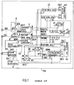
- Figure 1 shows a conventional (e.g., related art but not prior art) single-chip memory device 100 having a multiple bit line structure.
- the memory device 100 comprises a plurality of memory cell arrays m1 - mJ (where J is an integer greater than 2, and J is 16 in the case of X16, and J is 32 in the case of X32), and each of the memory cell arrays m1 - mJ has I (where I is an integer greater than 2) pairs of bit lines.
- sense amplifiers SAj1 - SAji (where j and i are integers, and 1 ⁇ j ⁇ J, 1 ⁇ i ⁇ I) are connected respectively to the pairs of bit lines of the memory cell array mj (where j is an integer, and 1 ⁇ j ⁇ J) for amplifying data from the memory cell array mj.
- sense amplifiers SA11 - SA1I are connected respectively to the pairs of bit lines of the memory cell array m1.
- Each of the sense amplifiers respectively outputs the amplified data to a corresponding pair of lines RBTi and RBNi (where i is an integer and 1 ⁇ i ⁇ I).
- sense amplifier SAJ1 outputs a high level signal (e.g., "1") and a low level signal (e.g., "0") respectively to a line RBT1 and a line RBN1.
- a plurality of first data amplifiers 30 respectively receive the corresponding signals on the pair of lines RBTi and RBNi, amplify these signals responsive to a corresponding first activation signal R1Pi (where i is an integer, 1 ⁇ i ⁇ I), and output amplified data to a corresponding pair of lines RWBTj and RWBNj (where j is an integer and 1 ⁇ j ⁇ J).
- Each of the first amplifiers 30 is activated when the corresponding first activation signal R1Pi has an active level (e.g., "1"), and is inactivated when the corresponding first activation signal R1Pi has an inactive level (e.g., "0").
- the pairs of the lines RWBTj and RWBNj are precharged by P-type metal oxide semiconductor (MOS) transistors P1 and P2, and these lines have parasitic capacitances C.
- MOS metal oxide semiconductor
- a signal generator 4 receives an address signal from an external device (e.g., an external central processing unit not shown in Figure 1) of the chip 100, and changes one of a plurality of second activation signals AS1 - ASI (where I is an integer greater than 2) to an active level (e.g., "1") from an inactive level (e.g., "0") corresponding to the address signal.
- the signal generator 4 also changes a third activation signal CS to an active level (e.g., "1") from an inactive level (e.g., "0") when the signal generator 4 receives an address signal.
- a plurality of first controllers 5 respectively change a corresponding signal of the first activation signals R1P1 - R1PI to an active level (e.g., "1") from an inactive level (e.g "0") when a corresponding signal of the second activation signals AS1 - ASI is changed to an active level from an inactive level.
- an active level e.g., "1”
- an inactive level e.g "0”
- a plurality of second data amplifiers 6 respectively receive and compare the signals on the corresponding pair of the lines RWBTj and RWBNj, and detect which line of the lines RWBTj and RWBNj has a higher voltage level. Then, the second data amplifier 6 changes the higher voltage level to a first reference voltage (e.g., Vcc) and changes the lower voltage level to a second reference voltage (e.g., ground level).
- a first reference voltage e.g., Vcc
- a second reference voltage e.g., ground level
- the second data amplifier 6 changes a voltage level of the line RWBTj to the first reference voltage level (Vcc), and changes a voltage level of the line RWBNj to the second reference voltage level (ground level) if the voltage level of the line RWBTj is higher than that of the line RWBNj when a fourth activation signal R2P has an active level (e.g., "1"). Then, the second data amplifier 6 outputs the first reference voltage level to a line RDTj corresponding to the line RWBTj, and outputs the second reference voltage to a line RDNj corresponding to the line RWBNj.
- a second controller 7 changes the fourth activation signal R2P to an active level (e.g "1") from an inactive level (e.g., "0") when the third activation signal CS is changed to an active level.
- a plurality of buffers 8 respectively comprising N-type MOS transistors N30 and N31, receive the corresponding signals RDTj and RDNj, and output signals DQj (where j is an integer and 1 ⁇ j ⁇ J) to output terminals (unreferenced).
- each first data amplifier 30 includes a differential amplifier 31 connected to the pair of lines RBTi and RBNi and which is activated in response to the first activation signal R1Pi.
- An inverter INV1 inverts the first activation signal R1Pi.
- An N-type MOS transistor N11 has a source-drain path between the lines RBTi and RBNi
- an N-type MOS transistor N12 has a source-drain path between the line RBNi and a first reference voltage (e.g., Vcc)
- an N-type MOS transistor N13 has a source-drain path between the line RBTi and the first reference voltage.
- a drain of N-type MOS transistor N1 is connected to the line RWBTj.
- a source of N-type MOS transistor N3 is connected to a second reference voltage (e.g., ground) and a drain of the MOS transistor N3 is connected to a source of the transistor N1.
- a drain of N-type MOS transistor N5 is connected to the line RWBNj.
- a source of N-type MOS transistor N6 is connected to the second reference voltage and a drain of the MOS transistor N6 is connected to a source of the transistor N5.
- Gates of the MOS transistors N11, N12 and N13 are connected to an output of the inverter INV1.
- Gates of the MOS transistors N3 and N6 are connected to an input of the inverter INV1.
- a gate of the MOS transistor N1 is connected to the line RBNi, and a gate of the MOS transistor N5 is connected to the line RBTi.
- Figure 2 is a timing chart for explaining an operation of reading data from memory cell arrays m1 - mJ.
- Vcc - VTN is a threshold voltage level of the MOS transistors N12 and N13.
- the signal generator 4 When the signal generator 4 receives an address signal, the signal generator 4 changes a corresponding signal of the second activation signals AS1 - ASI to an active level. In this example, a second activation signal AS1 is changed to an active level. Therefore, first controller 5 changes a first activation signal R1P1 to an active level, as shown in Figure 2.
- the memory cell arrays m1 - mJ also receive respectively the address signal (not shown in Figure 1) and output corresponding data. Therefore, sense amplifiers SA11 - SAJ1 respectively amplify corresponding data and output the data to corresponding pairs of lines RBT1 and RBN1.
- First data amplifiers 30 connected to the pairs of lines RBT1 and RBN1 are activated because the first activating signal R1P1 is changed to an active level. Therefore, first data amplifiers 30 respectively output amplified data to the corresponding pair of lines RWBTj and RWBNj, as shown in Figure 2.
- the second controller 7 changes the fourth activation signal R2P to an active level, as shown in Figure 2, because the signal generator 4 changes the third activation signal CS to an active level. Therefore, the second data amplifiers 6 respectively are activated, amplify the data on the corresponding pair of lines RWBTj and RWBNj, and output data to corresponding pairs of lines RDTj and RDNj, as shown in Figure 2.
- the memory device 100 outputs J (where J is 16 for an "X16" structure) data simultaneously when the device 100 receives an address signal.
- the number of lines RWBT1 - RWBTJ and RWBN1 - RWBNJ is (2 ⁇ J), which is two times larger than J which is the number of output data of the device 100. Therefore, it is difficult to make the device 100 smaller and more compact.
- Figure 3 shows another conventional (e.g., related art but not prior art) single-chip memory device having a decreased number of lines compared to the first conventional device.
- the same parts in Figure 3 as those in Figure 1 are numbered with the same reference numerals in Figure 1 and, for brevity, explanation of these parts are omitted from the following description.
- first data amplifiers 300 are activated when a corresponding first activation signal R1Pi is changed to an active level, amplify data on a corresponding pair of lines RBTi and RBNi, and output amplified data to a corresponding line RWBj.
- the number of lines RWB1 - RWBJ is half of the number of lines of the device shown in Figure 1.
- access timing T2 is later than the timing T1 of the device 100 shown in Figure 1.
- the first conventional system has adequate access speed, but is large and bulky.
- the second conventional system is smaller and more compact, but has a poor access speed.
- a memory system includes a plurality of memory cell arrays including a plurality of pairs of bit lines, a plurality of first bus lines corresponding to the plurality of memory cell arrays, a plurality of first data amplifiers for respectively amplifying data of corresponding pairs of bit lines and for outputting an amplified data to corresponding ones of the first bus lines, a reference voltage circuit for outputting a reference voltage level to a reference bus line, and a plurality of second data amplifiers, connected to corresponding ones of the first bus lines and the reference bus line, for receiving an output of the corresponding first data amplifier and the reference voltage level, for judging which voltage level is higher between the output of the corresponding first data amplifier and the reference voltage level, and for amplifying the voltage level being higher.
- the unique and unobvious structure of the present invention all of the second data amplifiers receive an output of the reference voltage circuit. Therefore, the number of bus lines can be decreased and the system size can be made smaller, as compared to the conventional memory system. Further, the memory system of the present invention can output data faster because the second data amplifier compares voltage levels of the outputs of the reference voltage circuit and the first data amplifier with one another. Therefore, an output of the first data amplifier need not be changed from ground level to the first voltage level of Vcc, and it can have a small amplitude.
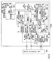
- a single-chip semiconductor memory system has a "multiple bit line" structure according to a first embodiment of the present invention.
- the same parts in Fig. 5 as those in Fig. 1 are numbered with the same reference numerals in Fig. 1 and, for brevity, explanations of these parts are omitted from the following description.
- FIG. 5 shows a single-chip memory device 1000 and an external central processing unit (CPU) 1001 for controlling the memory device 1000.
- the CPU 1001 outputs an address signal and executes an instruction using data from the device 1000.
- the memory device 1000 comprises a plurality of first data amplifiers 3000 respectively for receiving the signals on a corresponding pair of lines RBTi and RBNi, amplifying these signals responsive to a corresponding first activation signal R1Pi (where i is an integer and 1 ⁇ i ⁇ I) outputted by a first controller 5 discussed in further detail below, and outputting amplified data to a corresponding line RWBTj (where j is an integer and 1 ⁇ j ⁇ J).
- the lines RWBT1 - RWBTJ are precharged by P-type MOS transistor P1, and these lines have parasitic capacitances C.
- a line RWBR is connected to each of the second data amplifiers 6 instead of the lines RWBN1 - RWBNJ, as shown in Figure 1. As described below, such connection allows second data amplifiers 6 to compare the voltage levels of the outputs of the first data amplifiers 3000 with the outputs of a reference voltage circuit 9 to speed operation.
- the reference circuit 9 changes a signal on a line RWBR to a third reference voltage level when a fifth activation signal R1PR has an active level (e.g., "1") from an inactive level (e.g., "0).
- the reference circuit 9 comprises a P-type MOS transistor N91 having a source-drain path between the first reference voltage (e.g., Vcc) and the line RWBR and the gate is connected to the second reference voltage (e.g., ground level).
- a drain of an N-type MOS transistor N92 is connected to the line RWBR, and a drain of an N-type MOS transistor N93 is connected to a source of the MOS transistor N92.
- a source of the MOS transistor N93 is connected to the second reference voltage.
- An N-type MOS transistor N4 has a source-drain path between the first reference voltage and a gate of the MOS transistor N92, and a gate of the MOS transistor N4 is connected to the first reference voltage.
- a gate of the MOS transistor N93 is connected to the line R1PR.
- a reference controller 10 changes the fifth activation signal R1PR to an active level (e.g., "1") from an inactive level (e.g., "0") when the third activation signal CS changes to an active level.
- Each of the first data amplifiers 3000 is activated when the corresponding first activation signal R1Pi has an active level (e.g., "1"), and is inactivated when the corresponding first activation signal R1Pi has an inactive level (e.g., "0").
- an active level e.g., "1”
- an inactive level e.g., "0”
- Each first data amplifier 3000 includes differential amplifier 31 connected to the pair of lines RBTi and RBNi and which is activated in response to the corresponding first activation signal R1Pi.
- An inverter INV1 inverts the corresponding first activation signal R1Pi.
- An N-type MOS transistor N11 has a source-drain path between the lines RBTi and RBNi
- an N-type MOS transistor N12 has a source-drain path between the line RBNi and a first reference voltage (e.g., Vcc)
- an N-type MOS transistor N13 has a source-drain path between the line RBTi and the first reference voltage.
- a drain of N-type MOS transistor N1 is connected to the corresponding line RWBTj.
- a source of N-type MOS transistor N3 is connected to a second reference voltage (e.g., ground level) and a drain of the MOS transistor N3 is connected to a source of the transistor N1.
- a drain and a source of N-type MOS transistor N2 are connected to the second reference voltage.
- Gates of the MOS transistors N11, N12 and N13 are connected to an output of the inverter INV1.
- a gate of the MOS transistors N3 is connected to an input of the inverter INV1.
- a gate of the MOS transistor N2 is connected to the corresponding line RBTi, and a gate of the MOS transistor N1 is connected to the corresponding line RBNi.
- the MOS transistor N2 is used to adjust parasitic capacitances between the line RBNi and the line RBTi.
- Figure 6 is a timing chart for explaining an operation of reading data from memory cell arrays m1 - mJ.
- the lines RBWT1 - RWBTJ are precharged to a voltage level of Vcc, and the pairs of lines RBTi and RBNi are precharged to a voltage level (Vcc - VTN).
- VTN is a threshold voltage level of the MOS transistors N12 and N13.
- first controller 5 changes (and outputs) a first activation signal R1P1 to an active level, as shown in Figure 6.
- the reference controller 10 changes (and outputs) the fifth activation signal R1PR to an active level synchronizing with a first activation signal R1P1, as shown in Figure 6.
- the memory cell arrays m1 - mJ also receive respectively the address signal (not shown in Figure 5) and output corresponding data.
- the data is a pair of "True” (e.g., "1") and “Not” (e.g., "0") data. Therefore, sense amplifiers SA11 - SAJ1 respectively amplify corresponding data and output the data to corresponding pairs of lines RBT1 and RBN1.
- First data amplifiers 3000 connected to the pairs of lines RBT1 and RBN1, are activated because the first activating signal R1P1 is changed to an active level. Therefore, first data amplifiers 3000 respectively output amplified data to the corresponding line RWBTj, as shown in Figure 6.
- the second controller 7 changes (and outputs) the fourth activation signal R2P to an active level, as shown in Figure 6, because the signal generator 4 changes the third activation signal CS (not shown in Figure 6) to an active level. Therefore, the second data amplifiers 6 respectively are activated, amplify the data on the corresponding pair of lines RWBTj and RWBR, and output data to a corresponding pair of lines RDTj and RDNj, as shown in Figure 6.
- the memory device 1000 outputs J (where J is 16 for an "X16" structure) data simultaneously when the device receives an address signal from the CPU 1001.
- the differential amplifier 31 is designed so that the balance voltage level REF of the pair of lines RBTi and RBNi becomes an intermediate voltage level between the pair of lines RBTi and RBNi when differential amplifier 31 is activated.
- the chip 1000 has about half the number of lines as that of the related art device shown in Figure 1. Therefore, the chip can be made smaller than the related art device shown in Figure 1.
- data can be output faster than that of the related art system shown in Figure 3, because the first data amplifiers 3000 can output a signal having a small amplitude and do not have to output a signal having a large amplitude from ground to Vcc, as in the system of Figure 3.
- the device 1000 has low noise because the reference circuit 9 has a similar construction to the first data amplifier 3000.
- the reference circuit 9 has a similar construction to the first data amplifier 3000.
- the second data amplifier 6 might recognize erroneously that the signal on the line RWBTj is "True” when the signal is in fact "Not".
- the voltage levels of the line RWBTj and the line RWBR in the first embodiment of the present invention are shifted similarly because the reference circuit 9 has a similar construction to the first data amplifier 3000. Therefore, the second data amplifier 6 recognizes the level of the line RWBTj correctly.
- Figure 7 shows a single-chip memory system 2000 including an on-board CPU 2001.
- the CPU 2001 receives instructions from an input terminal (unreferenced), and executes the instructions by using data from a plurality of buffers 8.
- the CPU 2001 outputs an address signal to the signal generator 4 and a plurality of memory cell arrays m1 - mJ.
- the chip 2000 outputs data of a plurality of buffers 8 to an external device of the chip 2000 by using a plurality of terminals (unreferenced).
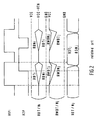
- Figure 8 shows an arrangement of the "X16" structure employable on either the chip 1000 or 2000.
- a "mirror" structure is formed in which eight buffers 8 are positioned at a first side and the other eight buffers 8 are positioned at a second side, as shown in Figure 8.
- line RWBR is longer than line RWBTj. Therefore, a parasitic capacitance CR of the line RWBR is larger than a parasitic capacitance C of the line RWBTj. Thus, a relatively long time is needed to change the line RWBR to the reference level REF1 if the parasitic capacitance CR is larger than the parasitic capacitance C. Therefore, in this case, the arrangement of Figure 8 preferably should be redesigned.
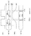
- Figure 9 shows another arrangement of the "X16" structure employable either on chip 1000 or 2000 including a reference circuit 9.
- a single reference circuit 9 provided in Figure 8
- two reference circuits 9 are provided on the chip 1000 (or 2000) to shorten the line RWBR. Therefore, the lines RWBT1 - RWBTJ and the lines RWBR have the same length, and parasitic capacitances CR and C have the same value.
- a device having the arrangement of Figure 9 can output data faster than a device having the arrangement of Figure 8.
- J and I depend on the memory system design. Thus, J could be sixteen for an "X16” structure, but alternatively it could be thirty-two for an "X32" structure.
- all of the second data amplifiers receive an output of the reference voltage circuit. Therefore, the number of bus lines can be decreased and the system size can be made smaller, as compared to the conventional (related art) memory systems.
- the memory system of the present invention can output data faster, because the second data amplifier compares voltage levels of the outputs of the reference voltage circuit and the first data amplifier with one another. Therefore, an output of the first data amplifier need not be changed from ground level to the first voltage level of Vcc, and it can have a small amplitude.
Landscapes
- Dram (AREA)
- Static Random-Access Memory (AREA)
Applications Claiming Priority (3)
| Application Number | Priority Date | Filing Date | Title |
|---|---|---|---|
| JP8041393A JP3008843B2 (ja) | 1996-02-28 | 1996-02-28 | 半導体記憶装置 |
| JP41393/96 | 1996-02-28 | ||
| JP4139396 | 1996-02-28 |
Publications (2)
| Publication Number | Publication Date |
|---|---|
| EP0809251A2 true EP0809251A2 (de) | 1997-11-26 |
| EP0809251A3 EP0809251A3 (de) | 1999-10-06 |
Family
ID=12607141
Family Applications (1)
| Application Number | Title | Priority Date | Filing Date |
|---|---|---|---|
| EP97103270A Withdrawn EP0809251A3 (de) | 1996-02-28 | 1997-02-27 | Einchipspeichersystem mit einer gruppierten Bitleitungsstruktur zur simultanen Ausgabe einer Mehrzahl von Daten |
Country Status (5)
| Country | Link |
|---|---|
| US (1) | US5784324A (de) |
| EP (1) | EP0809251A3 (de) |
| JP (1) | JP3008843B2 (de) |
| KR (1) | KR100232272B1 (de) |
| TW (1) | TW374924B (de) |
Families Citing this family (2)
| Publication number | Priority date | Publication date | Assignee | Title |
|---|---|---|---|---|
| US7196931B2 (en) * | 2002-09-24 | 2007-03-27 | Sandisk Corporation | Non-volatile memory and method with reduced source line bias errors |
| KR100956336B1 (ko) * | 2002-11-27 | 2010-05-06 | 삼성전자주식회사 | 박막 트랜지스터 기판의 제조 방법 |
Family Cites Families (5)
| Publication number | Priority date | Publication date | Assignee | Title |
|---|---|---|---|---|
| US4704678A (en) * | 1982-11-26 | 1987-11-03 | Inmos Limited | Function set for a microcomputer |
| KR910001744A (ko) * | 1988-06-14 | 1991-01-31 | 미다 가쓰시게 | 반도체 기억장치 |
| US5377143A (en) * | 1993-03-31 | 1994-12-27 | Sgs-Thomson Microelectronics, Inc. | Multiplexing sense amplifier having level shifter circuits |
| US5442748A (en) * | 1993-10-29 | 1995-08-15 | Sun Microsystems, Inc. | Architecture of output switching circuitry for frame buffer |
| US5526314A (en) * | 1994-12-09 | 1996-06-11 | International Business Machines Corporation | Two mode sense amplifier with latch |
-
1996
- 1996-02-28 JP JP8041393A patent/JP3008843B2/ja not_active Expired - Fee Related
-
1997
- 1997-02-26 US US08/806,667 patent/US5784324A/en not_active Expired - Lifetime
- 1997-02-27 EP EP97103270A patent/EP0809251A3/de not_active Withdrawn
- 1997-02-27 TW TW086102398A patent/TW374924B/zh not_active IP Right Cessation
- 1997-02-28 KR KR1019970006852A patent/KR100232272B1/ko not_active Expired - Fee Related
Also Published As
| Publication number | Publication date |
|---|---|
| KR100232272B1 (ko) | 1999-12-01 |
| KR970063249A (ko) | 1997-09-12 |
| US5784324A (en) | 1998-07-21 |
| EP0809251A3 (de) | 1999-10-06 |
| TW374924B (en) | 1999-11-21 |
| JPH09231759A (ja) | 1997-09-05 |
| JP3008843B2 (ja) | 2000-02-14 |
Similar Documents
| Publication | Publication Date | Title |
|---|---|---|
| US6144587A (en) | Semiconductor memory device | |
| KR100322540B1 (ko) | 입출력 센스앰프가 차지하는 면적을 최소화하는 메모리 장치 | |
| US5946253A (en) | Semiconductor memory device | |
| US6122220A (en) | Circuits and methods for generating internal signals for integrated circuits by dynamic inversion and resetting | |
| US6442077B2 (en) | Controlling reading from and writing to a semiconductor memory device | |
| KR930008311B1 (ko) | 센스 앰프의 출력 제어회로 | |
| US7269078B2 (en) | Buffer circuit and memory system for selectively outputting data strobe signal according to number of data bits | |
| US5784324A (en) | Single-chip memory system having a multiple bit line structure for outputting a plurality of data simultaneously | |
| USRE44051E1 (en) | Data bus line control circuit | |
| US6134174A (en) | Semiconductor memory for logic-hybrid memory | |
| US6157587A (en) | Data sense arrangement for random access memory | |
| JPH0922594A (ja) | データリード/ライト方法及びその装置 | |
| KR970003244A (ko) | 반도체 메모리 장치 | |
| KR100372246B1 (ko) | 반도체 메모리 장치의 에코클럭 생성회로 및 방법 | |
| US6031776A (en) | Sense amplifier circuit for a semiconductor memory device | |
| US6111813A (en) | Apparatus and method for tracking dynamic sense amplifier enable signals with memory array accessing signals in a synchronous RAM | |
| KR0164821B1 (ko) | 반도체 메모리 장치 | |
| KR100231430B1 (ko) | 반도체 메모리소자의 데이터출력 버퍼회로 | |
| US7075834B2 (en) | Semiconductor integrated circuit device | |
| KR100234368B1 (ko) | 병렬 비트 테스트 회로 | |
| US20050237819A1 (en) | Data output apparatus for memory device | |
| KR100316057B1 (ko) | 반도체 메모리 회로 | |
| US6091661A (en) | Data access device for DRAM | |
| US20010030902A1 (en) | Semiconductor memory for logic-hybrid memory | |
| JPH07130174A (ja) | 半導体装置 |
Legal Events
| Date | Code | Title | Description |
|---|---|---|---|
| PUAI | Public reference made under article 153(3) epc to a published international application that has entered the european phase |
Free format text: ORIGINAL CODE: 0009012 |
|
| AK | Designated contracting states |
Kind code of ref document: A2 Designated state(s): DE FR GB |
|
| PUAL | Search report despatched |
Free format text: ORIGINAL CODE: 0009013 |
|
| AK | Designated contracting states |
Kind code of ref document: A3 Designated state(s): DE FR GB |
|
| 17P | Request for examination filed |
Effective date: 19990901 |
|
| 17Q | First examination report despatched |
Effective date: 20010612 |
|
| RAP1 | Party data changed (applicant data changed or rights of an application transferred) |
Owner name: NEC ELECTRONICS CORPORATION Owner name: NEC CORPORATION |
|
| GRAP | Despatch of communication of intention to grant a patent |
Free format text: ORIGINAL CODE: EPIDOSNIGR1 |
|
| STAA | Information on the status of an ep patent application or granted ep patent |
Free format text: STATUS: THE APPLICATION HAS BEEN WITHDRAWN |
|
| 18W | Application withdrawn |
Effective date: 20031112 |