EP0807979A2 - Diode - Google Patents
Diode Download PDFInfo
- Publication number
- EP0807979A2 EP0807979A2 EP97107700A EP97107700A EP0807979A2 EP 0807979 A2 EP0807979 A2 EP 0807979A2 EP 97107700 A EP97107700 A EP 97107700A EP 97107700 A EP97107700 A EP 97107700A EP 0807979 A2 EP0807979 A2 EP 0807979A2
- Authority
- EP
- European Patent Office
- Prior art keywords
- diode
- mosfet
- region
- drain
- pseudo
- Prior art date
- Legal status (The legal status is an assumption and is not a legal conclusion. Google has not performed a legal analysis and makes no representation as to the accuracy of the status listed.)
- Withdrawn
Links
Images


Classifications
-
- H—ELECTRICITY
- H10—SEMICONDUCTOR DEVICES; ELECTRIC SOLID-STATE DEVICES NOT OTHERWISE PROVIDED FOR
- H10D—INORGANIC ELECTRIC SEMICONDUCTOR DEVICES
- H10D30/00—Field-effect transistors [FET]
- H10D30/60—Insulated-gate field-effect transistors [IGFET]
- H10D30/64—Double-diffused metal-oxide semiconductor [DMOS] FETs
- H10D30/66—Vertical DMOS [VDMOS] FETs
- H10D30/668—Vertical DMOS [VDMOS] FETs having trench gate electrodes, e.g. UMOS transistors
-
- H—ELECTRICITY
- H10—SEMICONDUCTOR DEVICES; ELECTRIC SOLID-STATE DEVICES NOT OTHERWISE PROVIDED FOR
- H10D—INORGANIC ELECTRIC SEMICONDUCTOR DEVICES
- H10D8/00—Diodes
-
- H—ELECTRICITY
- H10—SEMICONDUCTOR DEVICES; ELECTRIC SOLID-STATE DEVICES NOT OTHERWISE PROVIDED FOR
- H10D—INORGANIC ELECTRIC SEMICONDUCTOR DEVICES
- H10D84/00—Integrated devices formed in or on semiconductor substrates that comprise only semiconducting layers, e.g. on Si wafers or on GaAs-on-Si wafers
- H10D84/101—Integrated devices comprising main components and built-in components, e.g. IGBT having built-in freewheel diode
- H10D84/141—VDMOS having built-in components
-
- H—ELECTRICITY
- H10—SEMICONDUCTOR DEVICES; ELECTRIC SOLID-STATE DEVICES NOT OTHERWISE PROVIDED FOR
- H10D—INORGANIC ELECTRIC SEMICONDUCTOR DEVICES
- H10D84/00—Integrated devices formed in or on semiconductor substrates that comprise only semiconducting layers, e.g. on Si wafers or on GaAs-on-Si wafers
- H10D84/80—Integrated devices formed in or on semiconductor substrates that comprise only semiconducting layers, e.g. on Si wafers or on GaAs-on-Si wafers characterised by the integration of at least one component covered by groups H10D12/00 or H10D30/00, e.g. integration of IGFETs
- H10D84/811—Combinations of field-effect devices and one or more diodes, capacitors or resistors
Definitions
- This invention relates to voltage clamping devices and in particular to restricting current flows in PN diodes and MOS devices.
- a PN diode when forward biased, is a minority carrier device and, as such, has a long recovery time compared to majority carrier devices.
- a PN diode is reverse-biased under normal operation but can become temporarily forward-biased due to transients in the circuit.
- minority carriers are stored in the PN diode.
- the stored minority carriers increase the reverse recovery time of the PN diode (i.e., the time it takes a forward-biased diode to block a voltage applied in the reverse direction).
- a rapid voltage transient i.e., large dv/dt
- an parasitic PN diode (sometimes referred to as an "antiparallel" diode) is inherent in any MOSFET with a source-body short, the performance of any MOSFET can be degraded by the minority carriers of the PN diode.
- Quadrant I operation where the source terminal is connected to a lower voltage than the drain terminal
- the parasitic diode is reverse-biased and will conduct no current.
- the MOSFET should enter Quadrant III operation (where the source terminal is connected to a higher voltage than the drain terminal) the parasitic diode will become forward-biased and will conduct a current with minority carriers.
- the shorted terminal will be referred to as the "source” and the non-shorted terminal will be referred to as the "drain”.
- the term "electrical source” or “electrical drain” will be used.
- the "electrical source” is more negative than the "electrical drain”.
- the reverse is true.
- the current flowing through the parasitic diode may cause injection of minority carriers into the substrate of the IC. These minority carriers can travel through the substrate and cause various problems, such as latchup or snapback, in other devices throughout the IC.
- the current through the parasitic diode can introduce charges into the IC that become majority carriers in different regions of the IC. In this situation voltage drops will occur in the IC creating a "ground bounce" situation in the IC (i.e., spacially varying ground potentials), which can cause latchup problems.
- the current which would pass through the parasitic diode of the MOSFET during Quadrant III operation can be shunted away from the parasitic diode by placing a shunting device in parallel with the diode.
- a shunting device can also be used in parallel with any PN diode in order to prevent the problems caused by the minority carriers of a PN diode.
- the shunting device should conduct no current when the PN diode is reverse-biased and turn on at a lower voltage than the PN diode when the PN diode is forward-biased.
- silicon PN diodes Due to the physical properties of silicon, silicon PN diodes have a turn-on voltage of 0.6 to 0.8 V. Within this range, a higher forward-bias voltage corresponds to higher current densities and more stored minority carrier charge. Therefore, the shunting device should have a turn-on voltage less than 0.6 V. Furthermore, for the parasitic diode of a MOSFET, the shunting device should also have a low recovery time so that the turn-off time of the MOSFET will not be degraded by the shunting device.
- a Schottky diode is characterized by a low turn-on voltage (typically 0.2 to 0.3 volts), fast turn-off, and non-conductance when the Schottky diode is reverse-biased. Therefore, a Schottky diode can perform the functions of the shunting device.
- discrete Schottky diodes can be connected in parallel with the MOSFET or PN diode of the IC in a multi-chip solution.
- this type of connection there will exist various resistances, capacitances, and inductances within the connecting wires that may delay the Schottky diode's turn-on so that the parasitic or stand-alone PN diode will turn on before the Schottky diode.
- the use of discrete Schottky diodes is not ideal, since the clamping of the parasitic or stand-alone diode should be localized by placing the Schottky diode as close as possible to the parasitic or stand-alone diode.
- a shunting device which can be manufactured in an IC without requiring additional process steps, and which has the properties of turn-on voltage lower than a silicon diode, a fast recovery time when switched from a forward-bias to reverse-bias condition, and non-conductance under reverse bias.
- the shunting device could be merged into the power MOSFET itself without compromising the on-resistance or current density of the device.
- This invention makes use of the "body effect" which occurs in a MOSFET when the PN junction between the body and the drain (electrical source) of the MOSFET is partially forward-biased.
- the threshold voltage of the MOSFET is reduced, so that a relatively small voltage applied to the gate will cause a current to flow predominantly through the channel of the MOSFET, as compared to the parasitic diode that is formed at the body-drain junction.
- the gate-to-source voltage V gs that is necessary to turn the channel of the MOSFET on is reduced.
- the V gs required to turn the channel on is likewise reduced in an absolute sense (i.e., a less negative V gs is required).
- the MOSFET is fabricated as a four-terminal device, the body is properly biased in relation to the drain, and the gate is independently controlled (in an NMOS device, the drain being the terminal which is biased below the source).
- the MOSFET may be fabricated as a three-terminal device, with the body and source tied together and the gate independently controlled.
- the MOSFET is fabricated as a two-terminal device, with the body, gate and source tied together. Regardless of which configuration is used, if the MOSFET is properly biased it will turn on at a voltage which is substantially below the voltage at which a conventional PN diode will conduct current in the positive direction (i.e., 0.6-0.8 V).
- the two-terminal embodiment thus behaves like a diode which has a turn-on-voltage (at reasonable current densities) which is lower than that of a normal diode, although its turn-on voltage is not necessarily as low as that of a Schottky diode.
- the two-terminal device is referred to herein as a pseudo-Schottky diode , a name which will also be recognized as describing the physics of the MOSFET operation under certain conditions which make it behave more like a true Schottky diode than like a variable resistor.
- the performance of a pseudo-Schottky diode is improved to the extent that the body effect is maximized and the threshold voltage is minimized.
- the objective is to maximize the ratio of the channel current to the body-drain diode (PN junction) current, and to minimize the body-to-drain voltage.
- the MOSFET should have a high gain (G m ), a low on-resistance (R ds ), and a low threshold voltage (V t ).
- G m high gain
- R ds low on-resistance
- V t low threshold voltage
- the term "low on-resistance" is used in a somewhat unconventional sense, since the pseudo-Schottky diode conducts at a condition where the surface of the channel may not be fully inverted.
- Pseudo-Schottky (channel) conduction is significantly enhanced by designing the device to have a low threshold voltage, a thick gate oxide, a high body dopant concentration, a short channel length, and a large gate width per unit area.
- a threshold adjust ion implantation is typically required to offset the effect of those factors (e.g., high body doping and thick gate oxide) which tend to increase the threshold voltage.
- the threshold adjust ion implantation is performed prior to the formation of the gate.
- the threshold adjust implantation is performed either through the gate oxide and gate ( after any long, high-temperature furnace operation) or by introducing relatively immobile (slow diffusing) ions such as cesium into the gate oxide prior to the formation of the gate.
- a pseudo-Schottky diode of this invention has numerous uses.
- a pseudo-Schottky diode may be fabricated in parallel with other diodes and transistors in an integrated circuit (IC) chip. Since the pseudo-Schottky turns on at a lower voltage than a normal diode, it effectively clamps the other diodes in the forward direction. This limits charge storage and forward conduction in the other diodes, conditions which can lead to minority carrier injection, MOSFET snapback, and latchup of the IC chip.
- the pseudo-Schottky diode is also useful in switching mode power converters, where it can be used in place of a normal MOSFET that serves as a synchronous rectifier, to reduce the power loss and stored charge in the "break-before-make" interval which occurs before the gate is pulled high (assuming an N-channel device) to turn the MOSFET fully on.
- a normal MOSFET that serves as a synchronous rectifier
- a pair of pseudo-Schottky diodes can be used in place of the conventional bipolar transistor or MOSFET pair in a current mirror, thereby significantly reducing the voltage necessary to drive the current mirror.
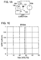
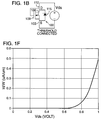
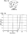
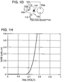
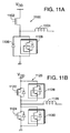
- Figs. 1A-1D illustrate circuit diagrams showing four possible ways of connecting a MOSFET as a two-terminal device.
- Figs. 1E-1H illustrate graphs showing the electrical characteristic of the configurations shown in Figs. 1A-1D, respectively.
- Fig. 2 illustrates a graph showing the threshold voltage (V t ) of a MOSFET as a function of the source-body voltage (V sb ) of the MOSFET.
- Fig. 3 illustrates a graph showing the drain current (I d ) as a function of the drain-source voltage (V ds ) at various levels of gate bias.
- Figs. 4A and 4B illustrate graphs which compare the IV characteristics of a pseudo-Schottky diode and a threshold connected MOSFET.
- Figs. 5A and 5B illustrate graphs which compare the IV characteristics of the a Schottky diode, a pseudo-Schottky diode, and an ideal PN diode.
- Fig. 6 illustrates a graph showing the voltage drop of a pseudo-Schottky diode under varying V t conditions.
- Fig. 7A illustrates a graph of a family of curves showing the snapback problem caused by the parasitic diode of a MOSFET.
- Fig. 7B illustrates a graph which shows the CMOS latchup problem caused by the parasitic diode of a MOSFET.
- Fig. 8 illustrates a cross-sectional view of an IC showing the use of a pseudo-Schottky diode to prevent diode recovery snapback caused by injection of minority carriers by the parasitic diode in an N-channel MOSFET.
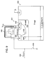
- Fig. 9 illustrates a cross-sectional view of an IC showing the use of a pseudo-Schottky diode to prevent snapback of a parasitic PNP bipolar transistor in a P-channel MOSFET.
- Fig. 10 illustrates a cross-sectional view of an IC showing the use of a pseudo-Schottky diode to prevent latchup of an IC caused by injection of minority carriers into the substrate by the parasitic diode.
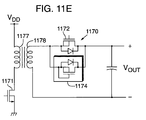
- Figs. 11A-11F illustrate circuit diagrams showing various uses of pseudo-Schottky diodes in power convertors.
- Fig. 11G illustrates a circuit diagram showing the use of a pseudo-Schottky diode in a current mirror arrangement.
- Figs. 12A-12C illustrate cross-sectional views showing three implementations of a pseudo-Schottky diode in integrated form.
- Fig. 13 illustrates a cross-sectional view of a pseudo-Schottky diode (with the source-gate short shown symbolically).
- Figs. 14A-14E illustrate cross-sectional views showing a method of forming an pseudo-Schottky diode based on a lateral MOSFET.
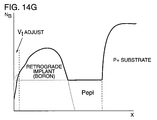
- Fig. 14F illustrates a graph showing a dopant concentration profile of the pseudo-Schottky diode of Fig. 14E.
- Fig. 14G illustrates a graph showing an alternative dopant concentration profile for the pseudo-Schottky diode of Fig. 14E.
- Figs. 15A-15C illustrate cross-sectional views showing a method of forming an pseudo-Schottky diode based on a vertical DMOSFET.
- Fig. 15D illustrates a graph showing the dopant concentration profile of the pseudo-Schottky diode of Fig. 15C.
- Fig. 16 illustrates a graph showing the log of the current (per unit gate width) versus the voltage between the terminals of a pseudo-Schottky diode as compared with those of a threshold-connected MOSFET (Fig. 1B).
- Fig. 17 illustrates a graph showing the current density in a pseudo-Schottky diode as a function of the body doping concentration for three gate oxide thicknesses (with the threshold voltage and the voltage across the diode being held constant).
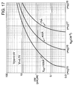
- Fig. 18 illustrates a graph showing lines of equal current density in a pseudo-Schottky diode as a function of both body doping concentration and gate oxide thickness (with the threshold voltage and the voltage across the diode being held constant).
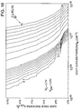
- Fig. 19 illustrates a graph containing two sets of curves showing the gate oxide thickness, body doping concentration and threshold adjust dose required to achieve three different current densities in a pseudo-Schottky diode.
- Fig. 20 illustrates a graph which compares the reverse recovery characteristics of a pseudo-Schottky diode with those of an ordinary P-N diode.
- Fig. 21 illustrates a graph which compares the measured reverse recovery time and the peak reverse current of a pseudo-Schottky diode with those of an ordinary P-N diode.
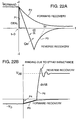
- Figs. 22A and 22B illustrate graphs showing the voltage and current waveforms in a diode during the recovery period following various types of switching.
- a pseudo-Schottky diode operates by making use of a phenomenon which is present in a low-threshold-voltage MOSFET operated with its body diode forward-biased and its gate enhanced. To understand this phenomenon, it is useful to consider the possible terminal configurations of a MOSFET.
- Figs. 1A-1D illustrate the four possible configurations of an N-channel MOSFET 100 as a two terminal device
- Figs. 1E-1H show the associated IV graphs of the devices.
- the shorted terminal will be referred to as the source and the non-shorted terminal will be referred to as the drain.
- Mosfet 100 also includes a body 106 and a gate 109.
- the reference numeral 115 designates the antiparallel diode which is inherent in MOSFET 100.
- the gate 109, the body 106 and the source terminal 103 are connected to negative voltage while the drain terminal 112 is connected to a positive voltage. Since the gate 109 is biased at the most negative potential, the channel of the MOSFET does not conduct. Furthermore, the parasitic diode 115 is reverse-biased and does not conduct.
- This configuration may be termed the "Off" configuration since under normal conditions no current flows through the MOSFET until the voltage reaches the breakdown voltage (BV dss ) of the antiparallel diode 115.
- the IV characteristic of MOSFET 100 connected as in Fig. 1A is shown in Fig. 1E, which shows a sharp current increase when the drain-to-source voltage V ds reaches the breakdown voltage BV dss of diode 115.
- the gate 109 and the drain terminal 112 are tied to the positive voltage while the body 106 and the source terminal 103 are tied to the negative voltage.
- the parasitic diode 115 remains reverse-biased and nonconductive.
- the gate 109 is tied to the positive power terminal, current will flow through the channel once the voltage reaches the threshold voltage V t of the MOSFET. This is designated the "Threshold-Connected" condition.
- the IV characteristic of MOSFET 100 connected as in Fig. 1B is shown in Fig. 1F, which shows a sharp current increase when V ds reaches approximately 0.8 V. While this connection gives a quick estimate of the MOSFET's threshold voltage, the true threshold voltage of the device must be determined by extrapolation methods that are described in numerous sources.
- Fig. 1C illustrates the "Diode-Connected" condition.
- the source terminal 103 and body 106 are connected to the positive voltage while the gate 109 and drain 112 are connected to the negative voltage. Since the gate 109 is connected to the most negative potential the channel of MOSFET 100 will not conduct a current. However, the parasitic diode 115, which is forward-biased, will conduct at its turn-on voltage V diode (0.6-0.8 Volts).
- the IV characteristic of MOSFET 100 connected as in Fig. 1C is shown in Fig. 1G, which shows a sharp current increase when V ds reaches V diode .
- Fig. 1D illustrates the "pseudo-Schottky" diode configuration of this invention.
- the gate 109, source terminal 103, and body 106 are all connected to the positive voltage, while only the drain terminal 112 is connected to the negative voltage.
- V PS pseudo-Schottky voltage
- the IV characteristic of MOSFET 100 connected as in Fig. 1D is shown in Fig. 1H, which shows a sharp current increase when V ds reaches V PS .
- Fig. 2 is a graph of the threshold voltage, V t of a four-terminal MOSFET (i.e., a MOSFET wherein the body is not shorted to either the source or the drain) as a function of the source-to-body voltage (V sb ) applied to the MOSFET.
- V sb source-to-body voltage
- the threshold voltage when the customary source-body short is present (V sb 0), is designated as V t0 .
- V t the threshold voltage of the MOSFET, is lower when V sb is negative (i.e., when the body is biased above the source).
- the cause of this change of the threshold voltage with V sb is called the "body effect".
- the body effect is commonly assumed to be an increase in threshold voltage resulting from reverse - biasing the source-to-body junction, but in the case of the pseudo-Schottky diode, the partial forward - biasing of the source-to-body junction (negative V sb ) leads to a lowering of V t , i.e., an "anti-body effect".
- the curves designated 3A, 3B, 3C and 3D in Fig. 3 show the drain-to-source current I d of a MOSFET as a function of the drain-to-source voltage (V ds ) at various positive gate biases (V gs ).
- V ds drain-to-source voltage
- V gs positive gate biases
- the source and body of the MOSFET are shorted together.
- the MOSFET acts essentially as a resistor until saturation is reached, and then the MOSFET acts as a constant current source.
- V PS represents I d as a function of V ds when the source (the more positive terminal in Quadrant III) is tied to the gate.
- the increasing gate bias relative to the drain (the most negative terminal in the MOSFET in Quadrant III)
- the body effect which results from the increasing potential of the body relative to the drain, and which reduces the threshold voltage V t (see Fig. 2), to cause the MOSFET to begin conducting at a voltage in the range of 0.2 to 0.3 V lower.
- curve V PS in Fig. 3 reveals that a MOSFET configured as shown in Fig. 1D behaves in the manner of a diode with a turn-on voltage which, while not normally as low as that of a true Schottky diode, is nonetheless significantly below the turn-on voltage of a conventional PN diode.
- the MOSFET of Fig. 1D is therefore referred to as a "pseudo-Schottky diode".
- the pseudo-Schottky diode has an anode at the terminal to which the body and gate of the MOSFET are tied and a cathode at the opposite terminal of the MOSFET.
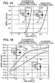
- Figs. 4A and 4B compare the drain-to-source current I d of a MOSFET (in ⁇ A/ ⁇ m of channel width) in Quadrant I operation versus the I d of a pseudo-Schottky diode (i.e., a device which exhibits the pseudo-Schottky effect) in Quadrant III operation.
- the curve designated PS relates to the pseudo-Schottky diode
- the curve designated M relates to the MOSFET.
- the gate of the MOSFET is tied to the more positive terminal of the MOSFET.
- FIG. 4A shows that due to the lower turn-on voltage of the pseudo-Schottky diode, the IV curve of the pseudo-Schottky diode is shifted towards the origin.
- Fig. 4B plots the log of I d to afford a better comparison of the currents, particularly in the subthreshold region of V ds .
- section A only leakage current is passing through both the pseudo-Schottky diode and the MOSFET, and therefore the currents are approximately equal.
- section B of the graph the pseudo-Schottky diode has turned on; therefore, the pseudo-Schottky current is much larger than the MOSFET current.
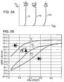
- Figs. 5A and 5B compare the IV characteristics of a Schottky diode (curve S), a pseudo-Schottky diode (curve PS), and a PN diode (curve PN).
- Fig. 5A plots I d and figure 5B plots log I d .
- a parasitic PN diode in a MOSFET will exhibit similar characteristics to the PN diode. As shown in Fig.
- the current through the pseudo-Schottky diode can be over 100 times greater than that of the PN diode. Therefore, for these voltages the pseudo-Schottky diode provides a very effective shunting device for a PN diode.
- Fig. 6 shows the voltage drop across a pseudo-Schottky diode (V DROP ) as a function of the current I for several threshold voltages V t of the MOSFET, where the threshold voltage is varied but the body effect is still pronounced. If a MOSFET has a high V t the body effect will be unable to lower the threshold enough for any significant conduction through the channel before the MOSFET's parasitic diode begins to conduct. For a low V t the body effect will lower the threshold of the MOSFET below the turn on voltage of the parasitic diode so that channel conduction will occur before the parasitic diode turns on. For medium V t channel conduction will occur to a lesser extent. The lower the threshold voltage, the higher the current density before the PN diode conduction overtakes the pseudo-Schottky (channel) conduction.
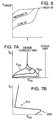
- Fig. 7A shows the IV characteristic of a MOSFET suffering from a snapback condition.
- V G1 , V G2 and V G3 represent different levels of gate drive voltage.
- V G1 , V G2 and V G3 represent different levels of gate drive voltage.
- the parasitic bipolar transistor of the MOSFET begins to conduct at a lower voltage than breakdown voltage of the MOSFET.
- each of the three curves in Fig. 7A represents a normal MOSFET IV characteristic. Snapback occurs, however, where the device enters a region of negative resistance as the bipolar transistor turns on, and thereafter the current increases dramatically.
- the shapes of the curves can vary in the transitional region where the curves merge.
- Fig. 7B shows the IV characteristic of an integrated circuit suffering from latchup.
- the MOSFET When the current reaches a certain point (designated 200 in Fig. 7B), the MOSFET will latch up and begin to conduct a sizeable current with almost no voltage drop (represented as region 201 in Fig. 7B). Even if the device survives the latchup current, the only way to restore normal operation is to momentarily remove the power from the device.
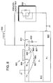
- Fig. 8 illustrates the use of a pseudo-Schottky diode to avoid a snapback condition.
- An N-channel MOSFET 800 shown in cross-section, is connected in a circuit which includes an inductor 830 connected to a drain 811 of MOSFET 800.
- Inductor 830 represents any inductance that is present in the circuit.
- MOSFET 800 includes an N+ source 809, which is shorted to a P-epitaxial layer 810 and a P+ substrate 820, and drain 811. P-epitaxial layer 810 and a P+ substrate 820 together form the body of MOSFET 800.
- the parasitic diode 802 When a negative voltage spike from inductor 830 drives drain 811 below ground, the parasitic diode 802 becomes forward-biased and injects minority carriers in the form of electrons 805 into P-epitaxial layer 810 and P+ substrate 820. While some of these electrons recombine with holes 807, or are collected by the source 809, the net result is that the entire region around drain 811 will be flooded with minority carriers. If the voltage on drain 811 is suddenly pulled positive again (either by inductor 830 or some other device), these minority carriers prevent the voltage from rising until they are removed or have recombined with holes. Once the minority carriers have been exhausted, the voltage will then rise very rapidly, causing a large dv/dt and a large displacement current.
- a pseudo-Schottky diode 850 is connected to MOSFET 800, with its "cathode” terminal 852 connected to drain 811 of MOSFET 800 and its “anode” terminal 854 connected to P+ substrate 820, which is grounded, the risk of snapback can be greatly reduced.
- pseudo-Schottky diode 850 will begin to conduct (through its channel) before the parasitic PN diode 802.
- the current will be shunted away from the MOSFET 800 by pseudo-Schottky diode 850. Consequently, the presence of minority carriers in MOSFET 800 will be greatly diminished.
- pseudo-Schottky diode 850 can be integrated with MOSFET 800, as will be explained later in this application.
- Fig. 9A illustrates snapback in a P-channel MOSFET 901, which is fabricated in a N-well 910 of an IC 900.
- the P+ source 904 and N+ body contact 902 are shorted together and tied to V cc .
- the P+ drain 906 is connected to an inductor 930 and a switch 935, which is tied to ground. When the switch 935 is opened, the voltage at the inductor 930 and the drain 906 will fly up above V cc . In this situation, the PN diode at the junction between P+ drain 906 and N-well 910 becomes forward-biased, which causes minority carriers in the form of holes 908 to be injected into N-well 910.
- a parasitic bipolar PNP transistor formed by the P+ drain 906 acting as the emitter, the N-well 910 acting as the base, and the P+ substrate 914 acting as the collector, has a base-to-collector voltage equal to V cc . Therefore, the parasitic PNP transistor will be turned on and will cause the snapback problem illustrated in Fig. 7A.
- MOSFET 901 can be clamped with an N-channel pseudo-Schottky diode 940 configured with its cathode connected to V cc and its anode connected to P+ drain 906. With pseudo-Schottky diode 940 in place when the switch 935 is opened and the inductor 930 pulls the drain 906 above V cc , pseudo-Schottky diode 940 will turn on before the parasitic PN diode turns on and clamp drain 906 at V cc . Alternatively, a P-channel pseudo-Schottky diode can be used in parallel with the MOSFET 901, or MOSFET 901 can be adjusted to exhibit the pseudo-Schottky effect itself.
- Fig. 10 illustrates a latchup condition that can occur in an integrated circuit 1000 which contains an N-channel MOSFET 1010 and a N-well 1020.
- An inductor 1040 is connected to the N+ drain 1011 of MOSFET 1010.
- the N+ source 1012 and P-epitaxial layer 1013 of the MOSFET 1010 are tied to ground.
- the inductor 1040 can pull the N+ drain 1011 below ground and thus forward-bias the parasitic diode formed by the P-epi layer 1013 and N+ drain 1011. Therefore, the drain 1011 will inject minority carriers in the form of electrons 1014 into the substrate. These electrons 1014 will recombine with holes 1016.
- the IR drop will in turn cause any grounded N+ region, such as source 1012, to be more negative than the surrounding P type material. Therefore the parasitic diode 1017, formed by the source 1012 and P-epi layer 1013, becomes forward-biased and injects minority carrier in the form of electrons 1018 of its own. These electrons 1018 may be collected by any N type material, where they will drift to the most positive potential that they can find. For example the electrons 1018 can be swept into the N-well 1020 and drift to the N+ region 1025 connected to V cc .
- the problem can be prevented by connecting the cathode of a pseudo-Schottky diode 1050 to N+ drain 1011 and connecting the anode of the pseudo-Schottky diode to ground.
- pseudo-Schottky diode 1050 when the inductor 1040 drives the drain 1011 below ground, pseudo-Schottky diode 1050 will shunt the electrons to ground, since pseudo-Schottky diode 1050 has a lower turn-on voltage than the parasitic PN diode formed by the junction of N+ drain 1011 and P-epi layer 1013. Without the electrons 1014 to forward-bias parasitic diode 1017, the latchup condition will not occur.
- pseudo-Schottky diode Another major use of the pseudo-Schottky diode is in power converters.
- Various power converter topologies are built around the relationships between a power source, an inductor, a load, and switches and diodes. In such topologies, the diodes are switched between being forward- and reverse-biased.
- a PN diode is a minority carrier device and will store minority carriers when it is forward-biased. When the diode is switched to reverse-bias, the stored charge can cause a long recovery time and large dv/dt.
- the manner in which it turns off is affected by the quantity of charge stored at its PN junction while it was conducting.
- the quantity of stored charge is proportional to the forward biased conduction current; the higher the forward bias, the greater the quantity of stored charge which must be depleted at turn-off. Therefore, the quantity of stored charge can be reduced by limiting the voltage drop across the diode when it is conducting current in the forward direction.
- Curve P2 shows what happens if the terminals of the diode are shorted. In this situation, the stored charge slows the turn-off.
- Curve P3 shows what happens if polarity of the voltage across the diode is suddenly reversed by applying a voltage V DD . The turn-off is accelerated somewhat, but at a penalty in behavior and performance.
- Fig. 22B is a plot of the voltage (V) versus time.
- Curve P5 corresponds to curve P2 in Fig. 22A and shows that the voltage across the diode decays exponentially from -V D when the terminals of the diode are shorted.
- Curve P6 corresponds to curve P3 in Fig.
- the charge stored near the junction of a conventional PN diode during forward conduction produces many undesirable effects. These effects can be reduced by using a pseudo-Schottky diode in place of or in parallel with the PN diode.
- a pseudo-Schottky diode can also be used in parallel with any intrinsic PN diode in a MOSFET, or the MOSFET itself can be designed to behave as a pseudo-Schottky diode.
- the pseudo-Schottky diode operates to reduce the voltage drop across a forward-biased PN junction. This in turn reduces the forward current across the PN junction and the quantity of charge that is stored near the junction during the period of forward conduction.
- Figs. 11A-11F show several power converter topologies which utilize pseudo-Schottky diodes to minimize minority carrier build up.
- Fig. 11A shows a buck converter 1100 comprising a high-side switch 1102, an inductor 1104, and a PN diode 1106 in parallel with a pseudo-Schottky diode 1108.
- the inductor 1104 whose current is constant so long as repeated switching occurs at a high frequency
- the diode handling the recirculating current is known as the rectifier.
- Fig. 11B shows a synchronous buck converter 1120 comprising a P-channel MOSFET 1122 in parallel with a pseudo-Schottky diode 1128, an inductor 1126, and an N-channel MOSFET 1124 acting as the rectifier in parallel with a pseudo-Schottky diode 1130.
- the P-channel MOSFET 1122 and the N-channel MOSFET 1124 are turned on off alternately, MOSFET 1122 being off when MOSFET 1124 is on and vice-versa.
- Fig. 11C illustrates a buck converter which includes a P-channel MOSFET 1144 acting as the high side switch and connected in parallel with a P-channel pseudo-Schottky diode 1142 in place of the N-channel pseudo-Schottky diode 1128 shown in Fig. 11B.
- Fig. 11D shows a boost converter 1150 which has a pseudo-Schottky diode 1152 in parallel with a rectifier diode 1154.
- the low-side switch 1151 is turned on so as to store energy in inductor 1156.
- Low-side switch 1151 is then turned off, causing the voltage at the drain of switch 1151 to fly above V out , thereby forward-biasing diode 1154.
- Feedback controls the "on" time of switch 1151 to hold V out constant.
- Pseudo-Schottky diode 1152 shunts current from diode 1154, reducing power losses and preventing forced diode recovery (i.e., the application of a reverse voltage to a diode which has charge stored from a previous forward conduction).
- Fig. 11E shows flyback converter 1170 with a MOSFET 1172 acting as a synchronous rectifier in parallel with a pseudo-Schottky diode 1174.
- low-side MOSFET 1171 is turned on to energize primary coil 1177.
- the turns in primary coil 1177 and secondary coil 1178 are oriented such that in this condition the intrinsic antiparallel diodes in MOSFET 1172 and pseudo-Schottky diode 1174 are reverse-biased and do not conduct current.
- MOSFETs 1171 and 1172 cannot be switched simultaneously because this would cause a "shoot through" current which would discharge the output capacitor.
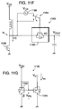
- Fig. 11F illustrates a circuit diagram of a circuit which includes a three-terminal MOSFET 1182 in accordance with another aspect of this invention.
- Switching-mode boost converter 1180 includes a switch 1184 which alternately connects the gate of MOSFET 1182 to either the source of MOSFET 1182 or a positive voltage V cp supplied by a charge pump 1186.
- a low-side MOSFET 1188 acts as a shunt switch. While low-side MOSFET 1188 is turned on, switch 1184 ties the gate and source of MOSFET 1182 together. Since at this time V out is higher than the voltage at node N, the channel in MOSFET 1182 is turned off and the intrinsic antiparallel diode within MOSFET 1182 is reverse-biased.
- MOSFET 1182 In the break-before-make interval between the turn-off of MOSFET 1188 and the turn-on of MOSFET 1182, the voltage at node N begins to fly up. During this interval, since the gate and source of MOSFET 1182 remain tied together, MOSFET 1182 exhibits the pseudo-Schottky effect and a current flows through the channel of MOSFET 1182, which constitutes a relatively low resistance path as compared to the path through the antiparallel diode of MOSFET 1182.
- the break-before-make interval ends when switch 1184 connects the gate of MOSFET 1182 to the voltage V cp supplied by charge pump 1186, thereby turning MOSFET 1182 fully on and providing a path for current to flow from node N towards the output terminal. With this arrangement, the IV power loss in MOSFET 1182 during the break-before-make interval is significantly less than would occur if, for example, the gate of MOSFET 1182 were grounded and the current flowed entirely through its antiparallel dio
- a pseudo-Schottky diode can be used in other types of converters, such as forward converters, where the pseudo-Schottky diode can be connected so as to shunt or replace a forward-conducting diode.
- a pseudo-Schottky diode may also be used in a current mirror, as shown in Fig. 11G.
- a current-mirror arrangement 1190 contains a pseudo-Schottky diode 1192 and a MOSFET 1194, whose drains and gates are tied together. The gate and source of pseudo-Schottky diode 1192 are tied together and to the positive supply voltage V dd .
- the mirror current I m is driven by a variable voltage V I .
- the current mirror ceases to function properly when V I falls to a voltage in the range of 0.7 V.
- the current mirror may also fail if V DD falls too low, e.g. around 0.7 V.
- current mirror arrangement 1190 operates with V I as low as about 0.4 V. While V I is restricted to a voltage less than a diode drop ( ⁇ 0.7 V), in many circuits this does not create a problem. For example, in a circuit supplied by a one-cell battery the supply voltage is about 0.9 V. Other components insure that the voltage across the pseudo-Schottky diode itself will not exceed 0.7 V, and it is very useful to have the current mirror function at voltages 0.2 V or so below the normal lower limit of 0.7 V.
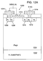
- Figs. 12A-12C illustrate cross-sectional views showing the structure of several embodiments of a pseudo-Schottky diode.
- Fig. 12A shows in cross-section an embodiment of a pseudo-Schottky diode 1200 formed in a lateral configuration.
- An P-epitaxial layer 1204 is grown upon a P+ substrate 1202 using conventional techniques.
- a P+ body contact 1206 and an N+ source 1208 are shorted by a metal source/body contact 1218.
- a gate 1216 is also connected to the source/body contact 1218, thus making the source/body contact 1218 the anode of pseudo-Schottky diode 1200.
- a metal drain contact 1214 which connects to the N+ drain 1212, is the cathode of pseudo-Schottky diode 1200.
- An N- drift region 1210 is located adjacent N+ drain 1212.
- Fig. 12B shows a pseudo-Schottky diode formed in a vertical trenched-gate configuration.
- the N+ substrate 1231 forms the drain of the MOSFET.
- An N-epitaxial layer 1232 is grown on N+ substrate 1231.
- a P-body region 1234 is implanted in N-epitaxial layer 1232.
- N+ source regions 1238 are implanted into P-body region 1234.
- a trench 1239 is then etched through the source and body regions and into the N-epitaxial layer 1232.
- the trench is filled with in gate 1236 which is separated from the N+ source 1230, P-body 1234, and N-epitaxial layer 1232 by a gate oxide layer 1240.
- a metal layer 1241 shorts the P-body and N+ source regions and is also connected to the gate 1236 to form the anode of pseudo-Schottky diode 1230.
- the N+ substrate 1231 which is also the drain, acts as the cathode of pseudo-Schottky diode 1230.
- Fig. 12C shows a pseudo-Schottky diode 1250 formed in a vertical double-diffused (DMOS) configuration.
- An N+ substrate 1251 acts as the drain of the MOSFET.
- An N-epitaxial layer 1252 is grown on the surface of the substrate 1251.
- P-body regions 1254 are implanted and diffused into the top surface of the N-epitaxial layer 1252.
- P+ body contact regions 1256 and N+ source regions 1258 are implanted and diffused into the P-body regions 1254.
- a gate 1260 overlies channel regions within P-body regions 1254.
- Gate 1260, P+ body contact regions 1256, and N+ source regions 1256 are connected to a metal layer 1262, which forms the anode of pseudo-Schottky diode 1250.
- N+ substrate 1251 serves as the cathode of pseudo-Schottky diode 1250.
- the doping concentrations and the gate oxide thickness are chosen so as to amplify the pseudo-Schottky effect.
- a threshold adjust implant will normally be required.
- the gate may be driven independently, but in most applications the gate will be connected to the source and body when the pseudo-Schottky diode is conducting, e.g., in the break-before-make intervals in the power converters shown in Figs. 11A-11F.
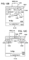
- Fig. 13 shows a cross-sectional view of a pseudo-Schottky diode 1300 in combination with a MOSFET 1302.
- An N-epitaxial layer 1312 is grown on an N+ substrate 1310.
- a P-body region 1314 is implanted into the N-epitaxial layer 1312.
- N+ source regions 1316 are implanted into the P-body region 1314.
- Trenches 1324 are then etched through the N+ source regions 1316 and P-body region 1314 and into the N-epitaxial layer 1312.
- the trenches 1324 are filled with a first gate 1318 or a second gate 1320, both of which are separated from N+ source regions 1316, P-body region 1314, and N-epitaxial layer 1312 by an oxide layer 1326.
- a metal layer 1322 contacts the P-body region 1314 and N+ source regions 1316, and is also connected to gate 1318.
- pseudo-Schottky diode 1300 is turned on and minimizes the storage of charge at the body-drain junction of MOSFET 1302.
- pseudo-Schottky diode 1300 used as a clamp in this way, current is instantaneously redistributed to pseudo-Schottky diode 1300 when it is forward-biased.
- the conventional MOSFET does not need to be made in accordance with the pseudo-Schottky method.
- the turn-on voltage of the pseudo-Schottky diode (V PS ) should be minimized relative to the turn-on voltage of the PN diode that is to be shunted.
- V t the threshold voltage of the MOSFET
- V to the extrapolated threshold voltage (i.e., the voltage where the MOSFET current extrapolates to zero)
- ⁇ the body effect factor (V -1/2 )
- I D sat ⁇ C ox 2 W L ⁇ V gs - [ V t 0 + ⁇ (
- V PS V t 0 + ⁇ (
- V PS V t 0 + ⁇ (
- V t0 also contains the terms X ox and N B , it is assumed here that a threshold adjusting ion implantation is used to adjust the threshold voltage to some target value to compensate for any changes in X ox and N B . Therefore, V t0 can be viewed as an independent variable.
- V PS is approximately 0.3 to 0.5 V, since ⁇ B is in the range of 0.65 V. Therefore, the second term of the V PS equation is positive but will lower V PS since it is subtracted from the first and third terms of the equation. Since V PS appears in the second term of the equation, to actually determine V PS the equation must be solved with an iterative process until the answer converges. However, the presence of V PS in the second term does not change the relationship that V PS is inversely proportional to the second term. The first and third terms are positive so that raising or lowering their values will lead to corresponding changes of V PS . As mentioned above, ideally V PS is as small as possible relative to the parasitic diode turn-on voltage. Without a threshold adjust implantation, V t0 is constrained by other factors and can not be used to control V PS . The two variables that can then be most easily adjusted in the equation for V PS are X ox and N B .
- V t0 is also increased if N B is increased.
- the threshold voltage V t is therefore generally adjusted by ion implantation to a final value in the range of 0.45 to 0.95 V, but generally between 0.6 and 0.7 V (no body effect).
- N B should be set to as high a value as possible given other required characteristics of the device such as breakdown voltage.
- a threshold adjust implant which is too high can lead to mobility denigration and an increase in on-resistance.
- Further improvement in V PS can be obtained by finding the optimal value of X ox for the given value of N B .
- the gate oxide must be kept thin to minimize on-resistance.
- the low-threshold voltage and simultaneous high body effect (which lowers the threshold voltage in Quadrant III operation) can be achieved by any method where a high concentration region of depth greater than the maximum depletion region from the gate (when inversion occurs) is counterdoped by a thin implanted layer or surface layer which is substantially depleted when the device is biased off.
- the threshold adjust implant For an N-channel device, the threshold adjust implant must be N-type dopant (arsenic or phosphorous) implanted into the silicon surface, or an immobile positive ion such as cesium implanted into the gate oxide.
- the dosage of the gate oxide charge must be increased if the charge is not located at the interface between the gate oxide and the silicon, e.g., a charge located halfway through the gate oxide requires twice the dosage to obtain the same shift of threshold voltage.
- kT/q is known as the thermal voltage (around 26 mV at room temperature) where k is Boltzmann's constant.
- n i is the intrinsic carrier concentration of silicon, having a value around 1.4 x 10 10 cm -3 at room temperature.
- Q f is the fixed oxide charge, around 2 x 10 10 cm -2 .
- Fig. 16 illustrates the challenges in developing a simple analytical model of the pseudo-Schottky effect.
- the gate width normalized current (I/W) is plotted as a function of V gs for the threshold-connected configuration (Fig. 1B) and the pseudo-Schottky configuration, assuming both a strong inversion model and a weak inversion model.
- Curves P7 and P8 represent the weak inversion model of the pseudo-Schottky and threshold-connected configurations, respectively; curves P9 and P10 represent the strong inversion model of the pseudo-Schottky and threshold-connected configurations, respectively.
- the previous equations are derived under the assumption that the silicon surface of an on-state MOSFET is strongly inverted.
- the normalized current for the weak inversion model is defined as follows: where ⁇ is the previously defined body effect factor, kT/q is the 26 mV thermal voltage, and the surface potential is now less than in strong inversion such that ⁇ sa ( V gb ) ⁇ - ⁇ 2 + ⁇ 2 4 + V gb - V FB 2
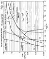
- Fig. 17 illustrates the pseudo-Schottky current I/W ( ⁇ A/ ⁇ m) as a function of background doping N B and gate oxide thickness.
- the threshold voltage V t was 0.7 V and the voltage across the diode V ps was 0.5 V.
- the three curves are for gate oxide thicknesses of 1000 ⁇ , 400 ⁇ and 175 ⁇ . While any device having a current over 0.1 ⁇ A/ ⁇ m with no more than a voltage drop of 0.5 V may be useful, a target current of at least 1 ⁇ A/ ⁇ m is needed for general purpose power devices.
- a L 2 ⁇ m 20 V lateral power NMOS having an on-resistance of 300 m ⁇ may have a 120,000 ⁇ m channel width and would be able to handle 120 mA of current in Quadrant III without substantial PN diode current or stored charge.
- a 1000 ⁇ thick gate oxide needs a background doping of 10 16 cm -3 to handle 1 ⁇ A/ ⁇ m of current
- a 400 ⁇ thick gate oxide needs a doping of 4 x 10 16 cm -3
- a 175 ⁇ thick gate oxide requires 1.5 x 10 17 cm -3 channel doping.
- gate oxide thicknesses above 500 ⁇ are not useful for MOSFETs used both as synchronous rectifiers and pseudo-Schottky diodes.
- Curve P12 represents the current in the pseudo-Schottky diode; curve P13 represents the current in the diode.
- Fig. 21 is a graph of I rr and t rr for a pseudo-Schottky diode and conventional PN diode, respectively, as a function of current and illustrates that the superiority in performance of the pseudo-Schottky diode is evident over a wide range of currents.
- the lefthand vertical axis shows the recovery time t rr in nanoseconds and the righthand vertical axis shows the peak reverse current I rr in mA.
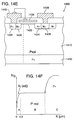
- Figs. 14A-14E show a sequence of manufacturing steps that can be used to obtain an pseudo-Schottky diode based on a lateral MOSFET.
- a P-epitaxial layer 1412, with a moderate dopant concentration e.g., 1 x 10 15 to 1 x 10 18 cm -3
- the magnitude of body doping needed to enhance the pseudo-Schottky effect is related to the gate oxide thickness.
- a 1000 ⁇ thick gate oxide can be useful for doping concentrations over 2 x 10 15 cm -3
- a gate oxide thickness of 400 ⁇ needs a minimum doping concentration of 1.5 x 10 16 cm -3 .
- a 175 ⁇ thick gate oxide needs a body doping concentration of at least 7 x 10 16 cm -3 to be useful.
- An oxide layer 1414 is used to define the active region of the device.
- An N-type counter dopant 1416 (phosphorous or arsenic) is implanted at the surface of P-epitaxial layer 1412, thereby forming a threshold adjust region 1422 wherein the net concentration of P-type dopant is lower than in the remainder of P-epitaxial layer 1412.
- a gate oxide layer 1417 and polysilicon gate 1418 have been formed over the counter-doped threshold adjust region 1422 using conventional techniques.
- the thickness of gate oxide layers may range from 80 ⁇ to 2000 ⁇ , but it is more commonly in the range of 175 ⁇ to 700 ⁇ .
- the polysilicon gate electrode is typically 1500 ⁇ to 6000 ⁇ thick and is generally doped with phosphorus for an N-channel device and with boron for a P-channel device. It may be shorted by a titanium or tungsten silicide layer.
- N-type dopant 1420 (phosphorus) is implanted into the exposed portions of P-epitaxial layer 1412 to form an N-drift region 1424 and an N- region 1425.
- the drift implant may be omitted for 5 V or less devices having a channel length of 2 ⁇ m or less, but a side wall spacer drift on the order of 0.25 long may be needed for devices having a submicron channel length.
- Fig. 14C shows the result of a third N-type implant, which forms an N+ source region 1426 and an N+ drain region 1428.
- N- region 1425 is converted into P+ body contact region 1432 in Fig. 14D by implanting a P-type dopant 1430 (boron).
- a photoresist layer 1434 prevents the boron implantation from reaching other areas of the device.
- Fig. 14E shows the resulting pseudo-schottky diode 1490 after a source/body metal contact layer 1440 and a drain metal contact layer 1438 are added.
- the gate 1418 is electrically connected to the source/body contact layer 1440 (but may also be driven independently).
- the source/body contact layer 1440 acts as the anode of pseudo-Schottky diode 1490, and drain contact layer 1438 acts as the cathode.
- Fig. 14F is a graph showing the dopant concentration N B of the device taken along a vertical section through the channel of pseudo-Schottky diode 1490 (shown by the dashed line in Fig. 14E).
- the abscissa of the graph of Fig. 14F is the distance in ⁇ m below the surface of the threshold-adjusted channel region.
- Region A includes the channel, wherein the concentration of P-type dopant has been lowered by the threshold adjust implant so as to lower the threshold voltage V t and thereby improve the turn-on characteristics of pseudo-Schottky diode 1490.
- Region B represents the P-epitaxial layer 1412
- Region C represents the P+ substrate 1410, which has the highest dopant concentration.
- Pseudo-Schottky diode 1490 can also be manufactured without the counter-doping implant shown in Fig. 14A, if a high energy implant step, as described in Application Serial No. 07/855,373 and Application Serial No. 07/854,162, is used to drive the dopant through the polysilicon gate.
- the sensitivity of the device characteristics to the level of epitaxial layer doping can be reduced by performing a second ion implantation (in addition to the counterdoping threshold voltage adjust) of the same conductivity type as the epitaxial layer itself. As shown in Fig.
- a retrograde boron implant at a dosage in the range of 1 x 10 12 to 5 x 10 14 cm -2 is implanted at 200 keV or greater to a mean depth of 0.2 to 1.0 ⁇ m below the surface of the epitaxial layer, so that less surface counterdoping is needed.
- the unimplanted portion of the P-epitaxial layer may be thin or nonexistent (the retrograde layer can extend into the substrate.
- the advantages of using ion implantation to set the value of N B and ⁇ instead of using the epitaxial layer alone include improved dopant concentration control and the ability to select which MOSFETs in an IC are to be adjusted for pseudo-Schottky enhancement.
- Figs. 15A-15C show a sequence of manufacturing steps that can be used to obtain an pseudo-Schottky diode based on a vertical DMOSFET.
- an N-epitaxial layer 1512 is grown on an N+ substrate 1510 which will be the cathode of the device.
- the doping level of the epitaxial layer is determined by the desired breakdown voltage of the device. For high voltage devices, concentrations of 1 x 10 14 to 1 x 10 15 cm -3 may be used while for lower voltages concentrations 1 x 10 15 to 1 x 10 16 cm -3 may be employed.
- P-body regions 1514 are formed in N-epitaxial layer 1512 using conventional techniques.
- a gate oxide layer 1516 and a polysilicon gate 1518 are also formed using conventional techniques of implantation and drive-in.
- Fig. 15B shows the addition of N+ source regions 1522 and P+ body contact regions 1524, also formed with conventional techniques.
- An N-type dopant 1520 (phosphorus) is then implanted at a dosage of 1 x 10 11 to 1 x 10 12 cm -2 and an energy of 300 keV to 2 MeV through gate 1518.
- Dopant 1520 forms counter-doped threshold adjust regions 1528 (Fig. 15C) at the surface of P-body regions 1514 in order to adjust the threshold voltage of the device.
- the phosphorous dopant will have little effect on the N-epitaxial layer 1512, since it should be located near the surface.
- Fig. 15C counter-doped threshold adjust regions 1528
- the pseudo-Schottky diode 1590 is substantially completed by adding a metal source/body contact layer 1526, which is also connected to gate 1518. These connections would not be made if device were a three-terminal or four-terminal MOSFET instead of a pseudo-Schottky diode.
- Fig. 15D shows the dopant concentration N B of the device at a section taken along the dashed line in Fig. 15C.
- region A represents the N+ source region 1522.
- Region B represents P-body region 1514.
- the concentration near the surface of the body region, shown as a dashed line in Fig. 15D, has been lowered due to the high energy counter-doping to adjust the threshold voltage V t .
- Region C represents N-epitaxial layer 1512
- Region D represents N+ substrate 1510.
Landscapes
- Metal-Oxide And Bipolar Metal-Oxide Semiconductor Integrated Circuits (AREA)
- Insulated Gate Type Field-Effect Transistor (AREA)
- Electronic Switches (AREA)
Applications Claiming Priority (2)
| Application Number | Priority Date | Filing Date | Title |
|---|---|---|---|
| US08/648,334 US5818084A (en) | 1996-05-15 | 1996-05-15 | Pseudo-Schottky diode |
| US648334 | 2000-08-25 |
Publications (2)
| Publication Number | Publication Date |
|---|---|
| EP0807979A2 true EP0807979A2 (de) | 1997-11-19 |
| EP0807979A3 EP0807979A3 (de) | 1998-02-25 |
Family
ID=24600393
Family Applications (1)
| Application Number | Title | Priority Date | Filing Date |
|---|---|---|---|
| EP97107700A Withdrawn EP0807979A3 (de) | 1996-05-15 | 1997-05-12 | Diode |
Country Status (2)
| Country | Link |
|---|---|
| US (2) | US5818084A (de) |
| EP (1) | EP0807979A3 (de) |
Cited By (7)
| Publication number | Priority date | Publication date | Assignee | Title |
|---|---|---|---|---|
| WO2009134812A1 (en) | 2008-04-28 | 2009-11-05 | Lakota Technologies, Inc. | Mosfet with integrated field effect rectifier |
| WO2012076231A3 (de) * | 2010-12-09 | 2012-09-07 | Robert Bosch Gmbh | Generatorvorrichtung zur spannungsversorgung eines kraftfahrzeugs |
| US8421118B2 (en) | 2007-09-26 | 2013-04-16 | Stmicroelectronics N.V. | Regenerative building block and diode bridge rectifier and methods |
| US8598620B2 (en) | 2007-09-26 | 2013-12-03 | Stmicroelectronics N.V. | MOSFET with integrated field effect rectifier |
| US8633521B2 (en) | 2007-09-26 | 2014-01-21 | Stmicroelectronics N.V. | Self-bootstrapping field effect diode structures and methods |
| US8643055B2 (en) | 2007-09-26 | 2014-02-04 | Stmicroelectronics N.V. | Series current limiter device |
| EP3770971A1 (de) * | 2019-07-26 | 2021-01-27 | Nexperia B.V. | Pseudo-schottky-diode |
Families Citing this family (144)
| Publication number | Priority date | Publication date | Assignee | Title |
|---|---|---|---|---|
| US5345170A (en) | 1992-06-11 | 1994-09-06 | Cascade Microtech, Inc. | Wafer probe station having integrated guarding, Kelvin connection and shielding systems |
| US6380751B2 (en) | 1992-06-11 | 2002-04-30 | Cascade Microtech, Inc. | Wafer probe station having environment control enclosure |
| US6232789B1 (en) | 1997-05-28 | 2001-05-15 | Cascade Microtech, Inc. | Probe holder for low current measurements |
| US5561377A (en) | 1995-04-14 | 1996-10-01 | Cascade Microtech, Inc. | System for evaluating probing networks |
| US5818084A (en) * | 1996-05-15 | 1998-10-06 | Siliconix Incorporated | Pseudo-Schottky diode |
| US5914613A (en) | 1996-08-08 | 1999-06-22 | Cascade Microtech, Inc. | Membrane probing system with local contact scrub |
| US5956578A (en) * | 1997-04-23 | 1999-09-21 | Motorola, Inc. | Method of fabricating vertical FET with Schottky diode |
| US6002263A (en) | 1997-06-06 | 1999-12-14 | Cascade Microtech, Inc. | Probe station having inner and outer shielding |
| US6150687A (en) | 1997-07-08 | 2000-11-21 | Micron Technology, Inc. | Memory cell having a vertical transistor with buried source/drain and dual gates |
| US6528837B2 (en) | 1997-10-06 | 2003-03-04 | Micron Technology, Inc. | Circuit and method for an open bit line memory cell with a vertical transistor and trench plate trench capacitor |
| US5914511A (en) * | 1997-10-06 | 1999-06-22 | Micron Technology, Inc. | Circuit and method for a folded bit line memory using trench plate capacitor cells with body bias contacts |
| US5907170A (en) | 1997-10-06 | 1999-05-25 | Micron Technology, Inc. | Circuit and method for an open bit line memory cell with a vertical transistor and trench plate trench capacitor |
| US6066869A (en) | 1997-10-06 | 2000-05-23 | Micron Technology, Inc. | Circuit and method for a folded bit line memory cell with vertical transistor and trench capacitor |
| US6031265A (en) * | 1997-10-16 | 2000-02-29 | Magepower Semiconductor Corp. | Enhancing DMOS device ruggedness by reducing transistor parasitic resistance and by inducing breakdown near gate runners and termination area |
| US6031702A (en) * | 1997-10-22 | 2000-02-29 | Siliconix Incorporated | Short circuit protected DC-DC converter using disconnect switching and method of protecting load against short circuits |
| US6268242B1 (en) * | 1997-12-31 | 2001-07-31 | Richard K. Williams | Method of forming vertical mosfet device having voltage clamped gate and self-aligned contact |
| US6172383B1 (en) | 1997-12-31 | 2001-01-09 | Siliconix Incorporated | Power MOSFET having voltage-clamped gate |
| US6025225A (en) | 1998-01-22 | 2000-02-15 | Micron Technology, Inc. | Circuits with a trench capacitor having micro-roughened semiconductor surfaces and methods for forming the same |
| US5963469A (en) | 1998-02-24 | 1999-10-05 | Micron Technology, Inc. | Vertical bipolar read access for low voltage memory cell |
| US6097242A (en) | 1998-02-26 | 2000-08-01 | Micron Technology, Inc. | Threshold voltage compensation circuits for low voltage and low power CMOS integrated circuits |
| US6124729A (en) | 1998-02-27 | 2000-09-26 | Micron Technology, Inc. | Field programmable logic arrays with vertical transistors |
| US5991225A (en) * | 1998-02-27 | 1999-11-23 | Micron Technology, Inc. | Programmable memory address decode array with vertical transistors |
| US6256882B1 (en) | 1998-07-14 | 2001-07-10 | Cascade Microtech, Inc. | Membrane probing system |
| US6134175A (en) | 1998-08-04 | 2000-10-17 | Micron Technology, Inc. | Memory address decode array with vertical transistors |
| US6208164B1 (en) | 1998-08-04 | 2001-03-27 | Micron Technology, Inc. | Programmable logic array with vertical transistors |
| US6724039B1 (en) * | 1998-08-31 | 2004-04-20 | Stmicroelectronics, Inc. | Semiconductor device having a Schottky diode |
| JP2000174135A (ja) * | 1998-12-07 | 2000-06-23 | Mitsubishi Electric Corp | 半導体装置及びその製造方法 |
| US6351018B1 (en) * | 1999-02-26 | 2002-02-26 | Fairchild Semiconductor Corporation | Monolithically integrated trench MOSFET and Schottky diode |
| US6498367B1 (en) * | 1999-04-01 | 2002-12-24 | Apd Semiconductor, Inc. | Discrete integrated circuit rectifier device |
| US6420225B1 (en) | 1999-04-01 | 2002-07-16 | Apd Semiconductor, Inc. | Method of fabricating power rectifier device |
| US6624030B2 (en) | 2000-12-19 | 2003-09-23 | Advanced Power Devices, Inc. | Method of fabricating power rectifier device having a laterally graded P-N junction for a channel region |
| US6448160B1 (en) | 1999-04-01 | 2002-09-10 | Apd Semiconductor, Inc. | Method of fabricating power rectifier device to vary operating parameters and resulting device |
| US6331455B1 (en) | 1999-04-01 | 2001-12-18 | Advanced Power Devices, Inc. | Power rectifier device and method of fabricating power rectifier devices |
| US6578264B1 (en) | 1999-06-04 | 2003-06-17 | Cascade Microtech, Inc. | Method for constructing a membrane probe using a depression |
| US6445202B1 (en) | 1999-06-30 | 2002-09-03 | Cascade Microtech, Inc. | Probe station thermal chuck with shielding for capacitive current |
| US6420757B1 (en) | 1999-09-14 | 2002-07-16 | Vram Technologies, Llc | Semiconductor diodes having low forward conduction voltage drop, low reverse current leakage, and high avalanche energy capability |
| US6433370B1 (en) | 2000-02-10 | 2002-08-13 | Vram Technologies, Llc | Method and apparatus for cylindrical semiconductor diodes |
| US6838890B2 (en) | 2000-02-25 | 2005-01-04 | Cascade Microtech, Inc. | Membrane probing system |
| WO2002007312A2 (en) | 2000-07-13 | 2002-01-24 | Isothermal Systems Research, Inc. | Power semiconductor switching devices, power converters, integrated circuit assemblies, integrated circuitry, power current switching methods, methods of forming a power semiconductor switching device, power conversion methods, power semiconductor switching device packaging methods, and methods of forming a power transistor |
| US6914423B2 (en) | 2000-09-05 | 2005-07-05 | Cascade Microtech, Inc. | Probe station |
| US6965226B2 (en) | 2000-09-05 | 2005-11-15 | Cascade Microtech, Inc. | Chuck for holding a device under test |
| US6580150B1 (en) | 2000-11-13 | 2003-06-17 | Vram Technologies, Llc | Vertical junction field effect semiconductor diodes |
| DE10143173A1 (de) | 2000-12-04 | 2002-06-06 | Cascade Microtech Inc | Wafersonde |
| US6537860B2 (en) | 2000-12-18 | 2003-03-25 | Apd Semiconductor, Inc. | Method of fabricating power VLSI diode devices |
| US6537921B2 (en) | 2001-05-23 | 2003-03-25 | Vram Technologies, Llc | Vertical metal oxide silicon field effect semiconductor diodes |
| WO2003052435A1 (en) | 2001-08-21 | 2003-06-26 | Cascade Microtech, Inc. | Membrane probing system |
| US6515330B1 (en) | 2002-01-02 | 2003-02-04 | Apd Semiconductor, Inc. | Power device having vertical current path with enhanced pinch-off for current limiting |
| US7078296B2 (en) | 2002-01-16 | 2006-07-18 | Fairchild Semiconductor Corporation | Self-aligned trench MOSFETs and methods for making the same |
| US6777964B2 (en) | 2002-01-25 | 2004-08-17 | Cascade Microtech, Inc. | Probe station |
| JP2005527823A (ja) | 2002-05-23 | 2005-09-15 | カスケード マイクロテック インコーポレイテッド | デバイスのテスト用プローブ |
| US6979861B2 (en) * | 2002-05-30 | 2005-12-27 | Apd Semiconductor, Inc. | Power device having reduced reverse bias leakage current |
| US6734495B2 (en) * | 2002-08-13 | 2004-05-11 | General Semiconductor, Inc. | Two terminal programmable MOS-gated current source |
| US6882573B2 (en) * | 2002-08-13 | 2005-04-19 | General Semiconductor, Inc. | DMOS device with a programmable threshold voltage |
| US7075763B2 (en) * | 2002-10-31 | 2006-07-11 | Micron Technology, Inc. | Methods, circuits, and applications using a resistor and a Schottky diode |
| US6847219B1 (en) | 2002-11-08 | 2005-01-25 | Cascade Microtech, Inc. | Probe station with low noise characteristics |
| US6724205B1 (en) | 2002-11-13 | 2004-04-20 | Cascade Microtech, Inc. | Probe for combined signals |
| US7250779B2 (en) | 2002-11-25 | 2007-07-31 | Cascade Microtech, Inc. | Probe station with low inductance path |
| US6861856B2 (en) | 2002-12-13 | 2005-03-01 | Cascade Microtech, Inc. | Guarded tub enclosure |
| US6958275B2 (en) * | 2003-03-11 | 2005-10-25 | Integrated Discrete Devices, Llc | MOSFET power transistors and methods |
| US7221172B2 (en) | 2003-05-06 | 2007-05-22 | Cascade Microtech, Inc. | Switched suspended conductor and connection |
| US7492172B2 (en) | 2003-05-23 | 2009-02-17 | Cascade Microtech, Inc. | Chuck for holding a device under test |
| US7057404B2 (en) | 2003-05-23 | 2006-06-06 | Sharp Laboratories Of America, Inc. | Shielded probe for testing a device under test |
| US7250626B2 (en) | 2003-10-22 | 2007-07-31 | Cascade Microtech, Inc. | Probe testing structure |
| US7187188B2 (en) | 2003-12-24 | 2007-03-06 | Cascade Microtech, Inc. | Chuck with integrated wafer support |
| DE202004021093U1 (de) | 2003-12-24 | 2006-09-28 | Cascade Microtech, Inc., Beaverton | Aktiver Halbleiterscheibenmessfühler |
| US6956429B1 (en) | 2004-02-09 | 2005-10-18 | Fairchild Semiconductor Corporation | Low dropout regulator using gate modulated diode |
| US7142046B1 (en) | 2004-05-14 | 2006-11-28 | Fairchild Semiconductor Corporation | Current sharing using gate modulated diodes |
| US7071518B2 (en) * | 2004-05-28 | 2006-07-04 | Freescale Semiconductor, Inc. | Schottky device |
| JP2008502167A (ja) | 2004-06-07 | 2008-01-24 | カスケード マイクロテック インコーポレイテッド | 熱光学チャック |
| US7330041B2 (en) | 2004-06-14 | 2008-02-12 | Cascade Microtech, Inc. | Localizing a temperature of a device for testing |
| US7355260B2 (en) * | 2004-06-30 | 2008-04-08 | Freescale Semiconductor, Inc. | Schottky device and method of forming |
| US7368927B2 (en) | 2004-07-07 | 2008-05-06 | Cascade Microtech, Inc. | Probe head having a membrane suspended probe |
| KR20070058522A (ko) | 2004-09-13 | 2007-06-08 | 캐스케이드 마이크로테크 인코포레이티드 | 양측 프루빙 구조 |
| US7250668B2 (en) * | 2005-01-20 | 2007-07-31 | Diodes, Inc. | Integrated circuit including power diode |
| US7535247B2 (en) | 2005-01-31 | 2009-05-19 | Cascade Microtech, Inc. | Interface for testing semiconductors |
| US7656172B2 (en) | 2005-01-31 | 2010-02-02 | Cascade Microtech, Inc. | System for testing semiconductors |
| US7126314B2 (en) * | 2005-02-04 | 2006-10-24 | Micrel, Incorporated | Non-synchronous boost converter including switched schottky diode for true disconnect |
| US7781826B2 (en) * | 2006-11-16 | 2010-08-24 | Alpha & Omega Semiconductor, Ltd. | Circuit configuration and manufacturing processes for vertical transient voltage suppressor (TVS) and EMI filter |
| US8110869B2 (en) * | 2005-02-11 | 2012-02-07 | Alpha & Omega Semiconductor, Ltd | Planar SRFET using no additional masks and layout method |
| US7282386B2 (en) * | 2005-04-29 | 2007-10-16 | Freescale Semiconductor, Inc. | Schottky device and method of forming |
| US7449899B2 (en) | 2005-06-08 | 2008-11-11 | Cascade Microtech, Inc. | Probe for high frequency signals |
| JP5080459B2 (ja) | 2005-06-13 | 2012-11-21 | カスケード マイクロテック インコーポレイテッド | 広帯域能動/受動差動信号プローブ |
| US7446374B2 (en) | 2006-03-24 | 2008-11-04 | Fairchild Semiconductor Corporation | High density trench FET with integrated Schottky diode and method of manufacture |
| DE202007018733U1 (de) | 2006-06-09 | 2009-03-26 | Cascade Microtech, Inc., Beaverton | Messfühler für differentielle Signale mit integrierter Symmetrieschaltung |
| JP4711894B2 (ja) * | 2006-06-09 | 2011-06-29 | 株式会社東芝 | 半導体装置 |
| US7764072B2 (en) | 2006-06-12 | 2010-07-27 | Cascade Microtech, Inc. | Differential signal probing system |
| US7443186B2 (en) | 2006-06-12 | 2008-10-28 | Cascade Microtech, Inc. | On-wafer test structures for differential signals |
| US7403028B2 (en) | 2006-06-12 | 2008-07-22 | Cascade Microtech, Inc. | Test structure and probe for differential signals |
| US7723999B2 (en) | 2006-06-12 | 2010-05-25 | Cascade Microtech, Inc. | Calibration structures for differential signal probing |
| KR100777445B1 (ko) * | 2006-07-28 | 2007-11-21 | 삼성전자주식회사 | 고주파 신호의 스위칭 장치 |
| US7895554B2 (en) * | 2006-12-21 | 2011-02-22 | Texas Instruments Incorporated | Verification method with the implementation of well voltage pseudo diodes |
| US8564057B1 (en) * | 2007-01-09 | 2013-10-22 | Maxpower Semiconductor, Inc. | Power devices, structures, components, and methods using lateral drift, fixed net charge, and shield |
| US7777257B2 (en) * | 2007-02-14 | 2010-08-17 | Freescale Semiconductor, Inc. | Bipolar Schottky diode and method |
| US7847315B2 (en) | 2007-03-09 | 2010-12-07 | Diodes Fabtech Inc. | High efficiency rectifier |
| US7876114B2 (en) | 2007-08-08 | 2011-01-25 | Cascade Microtech, Inc. | Differential waveguide probe |
| WO2009142897A1 (en) * | 2008-05-21 | 2009-11-26 | Fujifilm Corporation | Driving drop ejectors |
| US8022474B2 (en) | 2008-09-30 | 2011-09-20 | Infineon Technologies Austria Ag | Semiconductor device |
| US8203181B2 (en) | 2008-09-30 | 2012-06-19 | Infineon Technologies Austria Ag | Trench MOSFET semiconductor device and manufacturing method therefor |
| US7888957B2 (en) | 2008-10-06 | 2011-02-15 | Cascade Microtech, Inc. | Probing apparatus with impedance optimized interface |
| WO2010059247A2 (en) | 2008-11-21 | 2010-05-27 | Cascade Microtech, Inc. | Replaceable coupon for a probing apparatus |
| US8319503B2 (en) | 2008-11-24 | 2012-11-27 | Cascade Microtech, Inc. | Test apparatus for measuring a characteristic of a device under test |
| JP5172654B2 (ja) * | 2008-12-27 | 2013-03-27 | 株式会社東芝 | 半導体装置 |
| US8288820B2 (en) * | 2009-06-15 | 2012-10-16 | Texas Instruments Incorporated | High voltage power integrated circuit |
| US10205017B2 (en) * | 2009-06-17 | 2019-02-12 | Alpha And Omega Semiconductor Incorporated | Bottom source NMOS triggered Zener clamp for configuring an ultra-low voltage transient voltage suppressor (TVS) |
| TWI418015B (zh) * | 2010-05-13 | 2013-12-01 | 科軒微電子股份有限公司 | 具有場效整流元件之功率半導體結構及其製造方法 |
| CN102254944A (zh) | 2010-05-21 | 2011-11-23 | 上海新进半导体制造有限公司 | 一种沟槽mosfet功率整流器件及制造方法 |
| US8294210B2 (en) | 2010-06-15 | 2012-10-23 | Texas Instruments Incorporated | High voltage channel diode |
| JP5043990B2 (ja) * | 2010-06-18 | 2012-10-10 | シャープ株式会社 | 半導体装置およびその製造方法 |
| CN102315270B (zh) * | 2010-07-09 | 2013-04-24 | 科轩微电子股份有限公司 | 具有场效整流元件的功率半导体结构及其制造方法 |
| US8669613B2 (en) * | 2010-09-29 | 2014-03-11 | Alpha & Omega Semiconductor, Inc. | Semiconductor device die with integrated MOSFET and low forward voltage diode-connected enhancement mode JFET and method |
| CN102598265A (zh) | 2010-10-29 | 2012-07-18 | 松下电器产业株式会社 | 半导体元件 |
| JP5646360B2 (ja) * | 2011-02-04 | 2014-12-24 | 株式会社東芝 | 半導体装置 |
| JP5729331B2 (ja) * | 2011-04-12 | 2015-06-03 | 株式会社デンソー | 半導体装置の製造方法及び半導体装置 |
| CN103782390B (zh) * | 2011-08-11 | 2016-11-16 | 沃特拉半导体公司 | 垂直栅极射频横向扩散金氧半场效晶体管(ldmos)装置 |
| US9029956B2 (en) | 2011-10-26 | 2015-05-12 | Global Foundries, Inc. | SRAM cell with individual electrical device threshold control |
| US9048136B2 (en) | 2011-10-26 | 2015-06-02 | GlobalFoundries, Inc. | SRAM cell with individual electrical device threshold control |
| DE102012207654A1 (de) * | 2012-05-08 | 2013-11-14 | Robert Bosch Gmbh | Kraftfahrzeug-Generatorvorrichtung mit einer Schutzanordnung zur Störsignalunterdrückung |
| US9324625B2 (en) | 2012-05-31 | 2016-04-26 | Infineon Technologies Ag | Gated diode, battery charging assembly and generator assembly |
| US8587033B1 (en) | 2012-06-04 | 2013-11-19 | Infineon Technologies Austria Ag | Monolithically integrated HEMT and current protection device |
| US10290702B2 (en) | 2012-07-31 | 2019-05-14 | Silanna Asia Pte Ltd | Power device on bulk substrate |
| US9412881B2 (en) | 2012-07-31 | 2016-08-09 | Silanna Asia Pte Ltd | Power device integration on a common substrate |
| CN103199104B (zh) * | 2013-03-05 | 2016-04-27 | 矽力杰半导体技术(杭州)有限公司 | 一种晶圆结构以及应用其的功率器件 |
| CN103151371A (zh) | 2013-03-05 | 2013-06-12 | 矽力杰半导体技术(杭州)有限公司 | 一种晶圆结构以及应用其的功率器件 |
| DE102013204701A1 (de) * | 2013-03-18 | 2014-10-02 | Robert Bosch Gmbh | Pseudo-Schottky-Diode |
| US9620637B2 (en) * | 2013-05-24 | 2017-04-11 | Infineon Technologies Ag | Semiconductor device comprising a gate electrode connected to a source terminal |
| US9419116B2 (en) | 2014-01-22 | 2016-08-16 | Alexei Ankoudinov | Diodes and methods of manufacturing diodes |
| US9252293B2 (en) | 2014-01-22 | 2016-02-02 | Alexei Ankoudinov | Trench field effect diodes and methods of manufacturing those diodes |
| EP2940847A1 (de) * | 2014-04-30 | 2015-11-04 | Dialog Semiconductor GmbH | Verfahren und Vorrichtung für eine adaptive Schwelle eines Nulldurchgangkomparators, basierend auf dem Strom in den parasitären bipolaren Transistoren |
| US9324856B2 (en) | 2014-05-30 | 2016-04-26 | Texas Instruments Incorporated | MOSFET having dual-gate cells with an integrated channel diode |
| US9136381B1 (en) | 2014-11-18 | 2015-09-15 | Texas Instruments Incorporated | Super junction MOSFET with integrated channel diode |
| US9799645B2 (en) * | 2015-11-20 | 2017-10-24 | Raytheon Company | Field effect transistor (FET) structure with integrated gate connected diodes |
| TWI620333B (zh) * | 2015-12-08 | 2018-04-01 | 世界先進積體電路股份有限公司 | 肖特基二極體與其形成方法 |
| US9530900B1 (en) | 2016-01-26 | 2016-12-27 | Vanguard International Semiconductor Corporation | Schottky diode and method for manufacturing the same |
| CN105932072A (zh) * | 2016-07-06 | 2016-09-07 | 电子科技大学 | 一种积累型二极管 |
| US9923059B1 (en) | 2017-02-20 | 2018-03-20 | Silanna Asia Pte Ltd | Connection arrangements for integrated lateral diffusion field effect transistors |
| US10083897B2 (en) | 2017-02-20 | 2018-09-25 | Silanna Asia Pte Ltd | Connection arrangements for integrated lateral diffusion field effect transistors having a backside contact |
| CN107316863B (zh) * | 2017-07-12 | 2019-05-07 | 新昌县佳良制冷配件厂 | 瞬态电压抑制器及其制作方法 |
| US10297684B2 (en) * | 2017-09-29 | 2019-05-21 | Nxp Usa, Inc. | Bidirectional power MOSFET structure with a cathode short structure |
| CN108809284B (zh) * | 2017-10-27 | 2022-02-01 | 苏州捷芯威半导体有限公司 | 集成式功率开关器件和电子设备 |
| CN109755310B (zh) * | 2017-11-01 | 2021-01-01 | 苏州东微半导体有限公司 | 一种分栅结构的功率晶体管 |
| CN111742412B (zh) * | 2018-03-29 | 2023-09-15 | 新电元工业株式会社 | 宽带隙半导体装置 |
| US20190326900A1 (en) * | 2018-04-24 | 2019-10-24 | Infineon Technologies Ag | Driver circuit for a device circuit |
| DE102018132214A1 (de) * | 2018-12-14 | 2020-06-18 | Technische Hochschule Mittelhessen Körperschaft des öffentlichen Rechts | Steuerschaltung für eine Oszillatorschaltung zum Betrieb von parallelgespeisten Oszillatoren |
| CN114512402A (zh) * | 2022-04-19 | 2022-05-17 | 深圳芯能半导体技术有限公司 | 一种沟槽型碳化硅肖特基二极管及其制作方法 |
Family Cites Families (18)
| Publication number | Priority date | Publication date | Assignee | Title |
|---|---|---|---|---|
| JPS52132684A (en) * | 1976-04-29 | 1977-11-07 | Sony Corp | Insulating gate type field effect transistor |
| JPS5895856A (ja) * | 1981-12-02 | 1983-06-07 | Matsushita Electronics Corp | 半導体装置 |
| US4967243A (en) * | 1988-07-19 | 1990-10-30 | General Electric Company | Power transistor structure with high speed integral antiparallel Schottky diode |
| JPH0291974A (ja) * | 1988-09-29 | 1990-03-30 | Nippon Telegr & Teleph Corp <Ntt> | 半導体装置 |
| JP3111576B2 (ja) * | 1992-01-06 | 2000-11-27 | 富士電機株式会社 | 半導体装置 |
| US5248627A (en) * | 1992-03-20 | 1993-09-28 | Siliconix Incorporated | Threshold adjustment in fabricating vertical dmos devices |
| US5510641A (en) | 1992-06-01 | 1996-04-23 | University Of Washington | Majority carrier power diode |
| US5910669A (en) * | 1992-07-24 | 1999-06-08 | Siliconix Incorporated | Field effect Trench transistor having lightly doped epitaxial region on the surface portion thereof |
| GB9216953D0 (en) * | 1992-08-11 | 1992-09-23 | Philips Electronics Uk Ltd | A semiconductor component |
| US5414292A (en) * | 1993-05-26 | 1995-05-09 | Siliconix Incorporated | Junction-isolated floating diode |
| JPH07321306A (ja) * | 1994-03-31 | 1995-12-08 | Seiko Instr Inc | 半導体装置およびその製造方法 |
| JP3183020B2 (ja) * | 1994-03-17 | 2001-07-03 | 株式会社日立製作所 | 保護回路を内蔵した絶縁ゲート型半導体装置 |
| FR2723800B1 (fr) * | 1994-08-19 | 1997-01-03 | Thomson Csf Semiconducteurs | Circuit de protection contre les decharges electrostatiques |
| EP0773588B1 (de) * | 1995-11-10 | 2002-06-19 | Consorzio per la Ricerca sulla Microelettronica nel Mezzogiorno - CoRiMMe | Integriertes MOS-Bauelement mit einer Gateschutzdiode |
| JP3528420B2 (ja) * | 1996-04-26 | 2004-05-17 | 株式会社デンソー | 半導体装置およびその製造方法 |
| US5818084A (en) * | 1996-05-15 | 1998-10-06 | Siliconix Incorporated | Pseudo-Schottky diode |
| US6281547B1 (en) * | 1997-05-08 | 2001-08-28 | Megamos Corporation | Power transistor cells provided with reliable trenched source contacts connected to narrower source manufactured without a source mask |
| US6172398B1 (en) * | 1997-08-11 | 2001-01-09 | Magepower Semiconductor Corp. | Trenched DMOS device provided with body-dopant redistribution-compensation region for preventing punch through and adjusting threshold voltage |
-
1996
- 1996-05-15 US US08/648,334 patent/US5818084A/en not_active Expired - Lifetime
-
1997
- 1997-05-12 EP EP97107700A patent/EP0807979A3/de not_active Withdrawn
-
1998
- 1998-03-09 US US09/037,557 patent/US6476442B1/en not_active Expired - Lifetime
Cited By (13)
| Publication number | Priority date | Publication date | Assignee | Title |
|---|---|---|---|---|
| US8643055B2 (en) | 2007-09-26 | 2014-02-04 | Stmicroelectronics N.V. | Series current limiter device |
| US8421118B2 (en) | 2007-09-26 | 2013-04-16 | Stmicroelectronics N.V. | Regenerative building block and diode bridge rectifier and methods |
| US8598620B2 (en) | 2007-09-26 | 2013-12-03 | Stmicroelectronics N.V. | MOSFET with integrated field effect rectifier |
| US8633521B2 (en) | 2007-09-26 | 2014-01-21 | Stmicroelectronics N.V. | Self-bootstrapping field effect diode structures and methods |
| US9012954B2 (en) | 2007-09-26 | 2015-04-21 | STMicroelectronics International B.V. | Adjustable field effect rectifier |
| US9029921B2 (en) | 2007-09-26 | 2015-05-12 | Stmicroelectronics International N.V. | Self-bootstrapping field effect diode structures and methods |
| US9048308B2 (en) | 2007-09-26 | 2015-06-02 | Stmicroelectronics International N.V. | Regenerative building block and diode bridge rectifier and methods |
| EP2274770A4 (de) * | 2008-04-28 | 2012-12-26 | St Microelectronics Nv | Mosfet mit integriertem feldeffektgleichrichter |
| WO2009134812A1 (en) | 2008-04-28 | 2009-11-05 | Lakota Technologies, Inc. | Mosfet with integrated field effect rectifier |
| WO2012076231A3 (de) * | 2010-12-09 | 2012-09-07 | Robert Bosch Gmbh | Generatorvorrichtung zur spannungsversorgung eines kraftfahrzeugs |
| US9660550B2 (en) | 2010-12-09 | 2017-05-23 | Robert Bosch Gmbh | Generator device for the voltage supply of a motor vehicle |
| EP3770971A1 (de) * | 2019-07-26 | 2021-01-27 | Nexperia B.V. | Pseudo-schottky-diode |
| US11309409B2 (en) | 2019-07-26 | 2022-04-19 | Nexperia B.V. | Pseudo Schottky diode |
Also Published As
| Publication number | Publication date |
|---|---|
| US5818084A (en) | 1998-10-06 |
| EP0807979A3 (de) | 1998-02-25 |
| US6476442B1 (en) | 2002-11-05 |
Similar Documents
| Publication | Publication Date | Title |
|---|---|---|
| US6476442B1 (en) | Pseudo-Schottky diode | |
| US5929690A (en) | Three-terminal power MOSFET switch for use as synchronous rectifier or voltage clamp | |
| US6545316B1 (en) | MOSFET devices having linear transfer characteristics when operating in velocity saturation mode and methods of forming and operating same | |
| Barkhordarian | Power MOSFET basics | |
| KR100628938B1 (ko) | 개선된 고주파 스위칭 특성 및 항복 특성을 갖는 전력용반도체 장치들 | |
| US8598620B2 (en) | MOSFET with integrated field effect rectifier | |
| US6331794B1 (en) | Phase leg with depletion-mode device | |
| US8193570B2 (en) | Synchronous buck converter using shielded gate field effect transistors | |
| US20120212198A1 (en) | Semiconductor device | |
| US20070138547A1 (en) | Semiconductor device and method of manufacturing the same | |
| US11522453B2 (en) | Dead-time conduction loss reduction for buck power converters | |
| Siemieniec et al. | Stability and performance analysis of a SiC-based cascode switch and an alternative solution | |
| US20160197180A1 (en) | Power semiconductor transistor with improved gate charge | |
| US5585650A (en) | Semiconductor bidirectional switch and method of driving the same | |
| JP2011035292A (ja) | 半導体装置及び電源回路 | |
| US6940126B2 (en) | Field-effect-controllable semiconductor component and method for producing the semiconductor component | |
| US20190027598A1 (en) | Semiconductor device and circuit having the same | |
| US6538279B1 (en) | High-side switch with depletion-mode device | |
| Lutz et al. | MOS transistors and field controlled wide bandgap devices | |
| US20020070394A1 (en) | Using segmented N-type channel stop to enhance the SOA (safe-operating area) of LDMOS transistors | |
| CN102037548B (zh) | 具有集成场效应整流器的mosfet | |
| US10566452B2 (en) | Semiconductor device and control device | |
| Murakami et al. | Grounded-trench-MOS structure assisted normally-off bipolar-mode power FET | |
| Zambrano | Improved structures for power MOSFETs with on-chip full protection | |
| JPS6158264A (ja) | 半導体装置 |
Legal Events
| Date | Code | Title | Description |
|---|---|---|---|
| PUAI | Public reference made under article 153(3) epc to a published international application that has entered the european phase |
Free format text: ORIGINAL CODE: 0009012 |
|
| AK | Designated contracting states |
Kind code of ref document: A2 Designated state(s): DE FR GB IE IT NL |
|
| PUAL | Search report despatched |
Free format text: ORIGINAL CODE: 0009013 |
|
| AK | Designated contracting states |
Kind code of ref document: A3 Designated state(s): DE FR GB IE IT NL |
|
| 17P | Request for examination filed |
Effective date: 19980310 |
|
| 17Q | First examination report despatched |
Effective date: 20000322 |
|
| STAA | Information on the status of an ep patent application or granted ep patent |
Free format text: STATUS: THE APPLICATION IS DEEMED TO BE WITHDRAWN |
|
| 18D | Application deemed to be withdrawn |
Effective date: 20010828 |