EP0806686A1 - Verfahren und Vorrichtung zum Ausrichten und Fixieren von optischen Fasern - Google Patents
Verfahren und Vorrichtung zum Ausrichten und Fixieren von optischen Fasern Download PDFInfo
- Publication number
- EP0806686A1 EP0806686A1 EP97401031A EP97401031A EP0806686A1 EP 0806686 A1 EP0806686 A1 EP 0806686A1 EP 97401031 A EP97401031 A EP 97401031A EP 97401031 A EP97401031 A EP 97401031A EP 0806686 A1 EP0806686 A1 EP 0806686A1
- Authority
- EP
- European Patent Office
- Prior art keywords
- fiber
- groove
- substrate
- optical fiber
- widening
- Prior art date
- Legal status (The legal status is an assumption and is not a legal conclusion. Google has not performed a legal analysis and makes no representation as to the accuracy of the status listed.)
- Granted
Links
- 239000013307 optical fiber Substances 0.000 title claims description 49
- 238000000034 method Methods 0.000 title claims description 19
- 239000000835 fiber Substances 0.000 claims abstract description 66
- 239000000758 substrate Substances 0.000 claims abstract description 36
- 239000000853 adhesive Substances 0.000 claims abstract description 25
- 230000001070 adhesive effect Effects 0.000 claims abstract description 25
- 239000000126 substance Substances 0.000 claims description 17
- 238000010438 heat treatment Methods 0.000 claims description 6
- 238000012423 maintenance Methods 0.000 claims description 6
- 230000014759 maintenance of location Effects 0.000 abstract description 3
- 230000037431 insertion Effects 0.000 abstract 1
- 238000003780 insertion Methods 0.000 abstract 1
- 239000003292 glue Substances 0.000 description 11
- 230000003287 optical effect Effects 0.000 description 10
- VYPSYNLAJGMNEJ-UHFFFAOYSA-N Silicium dioxide Chemical compound O=[Si]=O VYPSYNLAJGMNEJ-UHFFFAOYSA-N 0.000 description 8
- 238000000151 deposition Methods 0.000 description 6
- XUIMIQQOPSSXEZ-UHFFFAOYSA-N Silicon Chemical compound [Si] XUIMIQQOPSSXEZ-UHFFFAOYSA-N 0.000 description 4
- 230000008021 deposition Effects 0.000 description 4
- 238000004518 low pressure chemical vapour deposition Methods 0.000 description 4
- 230000005855 radiation Effects 0.000 description 4
- OAICVXFJPJFONN-UHFFFAOYSA-N Phosphorus Chemical compound [P] OAICVXFJPJFONN-UHFFFAOYSA-N 0.000 description 3
- 238000009826 distribution Methods 0.000 description 3
- 238000005530 etching Methods 0.000 description 3
- 229910052710 silicon Inorganic materials 0.000 description 3
- 239000010703 silicon Substances 0.000 description 3
- 239000000377 silicon dioxide Substances 0.000 description 3
- 230000001133 acceleration Effects 0.000 description 2
- 230000008878 coupling Effects 0.000 description 2
- 238000010168 coupling process Methods 0.000 description 2
- 238000005859 coupling reaction Methods 0.000 description 2
- 238000004519 manufacturing process Methods 0.000 description 2
- 238000007254 oxidation reaction Methods 0.000 description 2
- 239000012071 phase Substances 0.000 description 2
- 229910052698 phosphorus Inorganic materials 0.000 description 2
- 239000011574 phosphorus Substances 0.000 description 2
- 238000001020 plasma etching Methods 0.000 description 2
- 229910052814 silicon oxide Inorganic materials 0.000 description 2
- XPDWGBQVDMORPB-UHFFFAOYSA-N Fluoroform Chemical compound FC(F)F XPDWGBQVDMORPB-UHFFFAOYSA-N 0.000 description 1
- 240000008042 Zea mays Species 0.000 description 1
- 238000004458 analytical method Methods 0.000 description 1
- QVGXLLKOCUKJST-UHFFFAOYSA-N atomic oxygen Chemical compound [O] QVGXLLKOCUKJST-UHFFFAOYSA-N 0.000 description 1
- 230000015572 biosynthetic process Effects 0.000 description 1
- 238000005234 chemical deposition Methods 0.000 description 1
- 238000003776 cleavage reaction Methods 0.000 description 1
- 238000009792 diffusion process Methods 0.000 description 1
- 238000006073 displacement reaction Methods 0.000 description 1
- 238000001312 dry etching Methods 0.000 description 1
- 230000000694 effects Effects 0.000 description 1
- 229920006332 epoxy adhesive Polymers 0.000 description 1
- 239000012530 fluid Substances 0.000 description 1
- 238000003384 imaging method Methods 0.000 description 1
- 230000000873 masking effect Effects 0.000 description 1
- 239000000463 material Substances 0.000 description 1
- 238000002844 melting Methods 0.000 description 1
- 230000008018 melting Effects 0.000 description 1
- 229910021421 monocrystalline silicon Inorganic materials 0.000 description 1
- 238000000465 moulding Methods 0.000 description 1
- 230000003647 oxidation Effects 0.000 description 1
- 229910052760 oxygen Inorganic materials 0.000 description 1
- 239000001301 oxygen Substances 0.000 description 1
- 238000000206 photolithography Methods 0.000 description 1
- 229920000642 polymer Polymers 0.000 description 1
- 229920005989 resin Polymers 0.000 description 1
- 239000011347 resin Substances 0.000 description 1
- 230000007017 scission Effects 0.000 description 1
- 239000012808 vapor phase Substances 0.000 description 1
- 238000001039 wet etching Methods 0.000 description 1
Images


Classifications
-
- G—PHYSICS
- G02—OPTICS
- G02B—OPTICAL ELEMENTS, SYSTEMS OR APPARATUS
- G02B6/00—Light guides; Structural details of arrangements comprising light guides and other optical elements, e.g. couplings
- G02B6/24—Coupling light guides
- G02B6/36—Mechanical coupling means
- G02B6/3628—Mechanical coupling means for mounting fibres to supporting carriers
- G02B6/3632—Mechanical coupling means for mounting fibres to supporting carriers characterised by the cross-sectional shape of the mechanical coupling means
- G02B6/3636—Mechanical coupling means for mounting fibres to supporting carriers characterised by the cross-sectional shape of the mechanical coupling means the mechanical coupling means being grooves
-
- G—PHYSICS
- G02—OPTICS
- G02B—OPTICAL ELEMENTS, SYSTEMS OR APPARATUS
- G02B6/00—Light guides; Structural details of arrangements comprising light guides and other optical elements, e.g. couplings
- G02B6/10—Light guides; Structural details of arrangements comprising light guides and other optical elements, e.g. couplings of the optical waveguide type
- G02B6/12—Light guides; Structural details of arrangements comprising light guides and other optical elements, e.g. couplings of the optical waveguide type of the integrated circuit kind
- G02B6/122—Basic optical elements, e.g. light-guiding paths
-
- G—PHYSICS
- G02—OPTICS
- G02B—OPTICAL ELEMENTS, SYSTEMS OR APPARATUS
- G02B6/00—Light guides; Structural details of arrangements comprising light guides and other optical elements, e.g. couplings
- G02B6/24—Coupling light guides
- G02B6/36—Mechanical coupling means
- G02B6/3616—Holders, macro size fixtures for mechanically holding or positioning fibres, e.g. on an optical bench
- G02B6/362—Vacuum holders for optical elements
-
- G—PHYSICS
- G02—OPTICS
- G02B—OPTICAL ELEMENTS, SYSTEMS OR APPARATUS
- G02B6/00—Light guides; Structural details of arrangements comprising light guides and other optical elements, e.g. couplings
- G02B6/24—Coupling light guides
- G02B6/26—Optical coupling means
- G02B6/28—Optical coupling means having data bus means, i.e. plural waveguides interconnected and providing an inherently bidirectional system by mixing and splitting signals
- G02B6/2804—Optical coupling means having data bus means, i.e. plural waveguides interconnected and providing an inherently bidirectional system by mixing and splitting signals forming multipart couplers without wavelength selective elements, e.g. "T" couplers, star couplers
- G02B6/2808—Optical coupling means having data bus means, i.e. plural waveguides interconnected and providing an inherently bidirectional system by mixing and splitting signals forming multipart couplers without wavelength selective elements, e.g. "T" couplers, star couplers using a mixing element which evenly distributes an input signal over a number of outputs
- G02B6/2813—Optical coupling means having data bus means, i.e. plural waveguides interconnected and providing an inherently bidirectional system by mixing and splitting signals forming multipart couplers without wavelength selective elements, e.g. "T" couplers, star couplers using a mixing element which evenly distributes an input signal over a number of outputs based on multimode interference effect, i.e. self-imaging
-
- G—PHYSICS
- G02—OPTICS
- G02B—OPTICAL ELEMENTS, SYSTEMS OR APPARATUS
- G02B6/00—Light guides; Structural details of arrangements comprising light guides and other optical elements, e.g. couplings
- G02B6/24—Coupling light guides
- G02B6/36—Mechanical coupling means
- G02B6/38—Mechanical coupling means having fibre to fibre mating means
- G02B6/3807—Dismountable connectors, i.e. comprising plugs
- G02B6/3833—Details of mounting fibres in ferrules; Assembly methods; Manufacture
- G02B6/3834—Means for centering or aligning the light guide within the ferrule
- G02B6/3838—Means for centering or aligning the light guide within the ferrule using grooves for light guides
- G02B6/3839—Means for centering or aligning the light guide within the ferrule using grooves for light guides for a plurality of light guides
-
- G—PHYSICS
- G02—OPTICS
- G02B—OPTICAL ELEMENTS, SYSTEMS OR APPARATUS
- G02B6/00—Light guides; Structural details of arrangements comprising light guides and other optical elements, e.g. couplings
- G02B6/24—Coupling light guides
- G02B6/36—Mechanical coupling means
- G02B6/38—Mechanical coupling means having fibre to fibre mating means
- G02B6/3807—Dismountable connectors, i.e. comprising plugs
- G02B6/3833—Details of mounting fibres in ferrules; Assembly methods; Manufacture
- G02B6/3855—Details of mounting fibres in ferrules; Assembly methods; Manufacture characterised by the method of anchoring or fixing the fibre within the ferrule
- G02B6/3861—Adhesive bonding
Definitions
- the present invention relates to the field of positioning and maintaining optical fibers. It applies in particular in the field of integrated optics, where optical fibers are means suitable for coupling and decoupling light in and from integrated optical components. More specifically, such coupling and decoupling problems arise when the integrated optical components include optical microguides. Due to the relatively small dimensions, both of the integrated optical components, in particular of the microguides, and of the optical fiber, it is necessary to use mechanical structures to achieve a relatively precise positioning of the two elements one opposite the other.
- the document FR-2 659 148 describes a method of connection between an optical fiber and an optical microguide.
- only one support is used, namely the substrate on which the optical microguide is made, and in which a housing is made to position and hold the optical fiber in front of this microguide.
- the technique described in this prior art has a drawback, since nothing is provided to facilitate the deposition of glue once the fiber is placed in position.
- a second drawback concerns the gripping of the fiber, and the size of the gripping system: the gripping of the fiber can only be done on the upper half-cylinder, defined by the upper part of the fiber.
- the device essentially comprises a substrate 2 in which grooves 4-1, ... 4-n are etched, for positioning n optical fibers 8-1, ... 8-n.
- a drop of glue 10 is deposited on said fiber.
- a transverse trench 6 is made to prevent the diffusion of the adhesive between two zones 12, 14 located on either side of the trench.
- the glue is introduced into at least one of the two zones but not into the trench.
- nothing is provided in this device to facilitate the deposition of the adhesive after positioning the fiber.
- such a structure allows the gripping of the fiber only on a part of the upper half-cylinder thereof with a gripping system of limited size (the problem of the size of the gripping system n was not taken into account).
- the invention relates to a device allowing precise positioning of an optical fiber on a substrate, improved deposition of the adhesive between the fiber and the substrate, and better retention of the fiber during positioning and bonding operations.
- the subject of the invention is a device for positioning and maintaining an optical fiber, comprising a substrate, a groove intended to receive an optical fiber, and at least first and second enlargements of the groove, along of a longitudinal axis of the latter.
- One or other of the enlargements of the groove makes it possible to deposit the glue in the bottom of the structure for holding the fiber, or substrate. Indeed, this widening leaves a free space between the fiber and the substrate, by which the adhesive can be introduced before and / or after the positioning of the fiber in the groove.
- the other enlargement makes it possible to hold the fiber with a more bulky gripping or handling tool which can hold the fiber over a larger circumference than in the case of the devices of the prior art.
- adheresive means any adhesive substance relative to the surface of the substrate and to that of the fiber.
- the invention also relates to a device for positioning and holding N optical fibers, comprising a substrate, N parallel grooves each intended to receive an optical fiber and each having a longitudinal axis and at least a first and a second widening of each groove, along its longitudinal axis.
- the first widening of at least one groove can be provided communicating with the first widening of at least one neighboring groove.
- the second widening of at least one groove can be provided communicating with the second widening of at least one neighboring groove.
- the step of introducing the adhesive can be carried out before positioning the fiber in the groove and / or after the latter has been maintained in the widening of the groove. Furthermore, the step of positioning the fiber in the groove can be confused with the holding step (the gripping step then makes it possible to bring the fiber into the groove). In this case, the tool allows both positioning and holding. This tool, after hardening of the glue, is separated from the fiber. Thus, the invention allows precise maintenance of the fiber during the bonding phase.
- the invention also relates to various tools for positioning and holding a fiber, which can be used with a device according to the invention.
- FIG. 2A illustrates a first embodiment of the invention.
- a groove 22 is formed in a substrate 20.
- At least two notches 24, 26 define enlargements of the groove 22.
- the latter has substantially the same dimension as an optical fiber 28 intended to be positioned there.
- a space is provided between the internal edges 30 of the substrate 20 and the optical fiber 28.
- a gripping tool and bulky holding of the fiber is positioned at the height of one of the enlargements, while glue can be introduced, in the other enlargement, between the inner edges of the substrate and the optical fiber.
- the glue penetrates better below the latter.
- Figure 2B shows a section of the device of Figure 2A along axis II. It is clear from this figure that, thanks to the widening 26, the fiber 28 can be maintained not only along the upper half-cylinder (of trace AB in FIG. 2B), but also along the lateral surfaces, of trace AC and BD in Figure 2B. Better support is therefore ensured during bonding operations.
- the invention allows maintenance over a larger area of the fiber, it is however not limited to such maintenance. Indeed, a maintenance on part of the track surface AB may be sufficient.
- the enlargements may have ends that are bounded, or closed (as in FIGS. 2A and 2B) or else unbounded. Depending on the viscosity of the adhesive substance or glue used, it may be preferable to use narrow enlargements.
- FIGS. 3A and 3B Two examples of positioning and holding tools that can be used are illustrated in FIGS. 3A and 3B.
- the fiber 28 is maintained using a gripping tool 21 which has a head 23 whose width L is greater than the diameter of the fiber.
- the fiber is wedged between two cheeks, or uprights, 27, 37. This tool allows a hold on the upper half-cylinder. Variants of this tool can be made to have a significant hold on a surface less than the half-cylinder.
- the tool of FIG. 3B in fact comprises a heating tip 29 and a layer of wax 31. This tool allows it to be held on a larger surface than the upper half-cylinder (of trace AB). The tool is then released by heating to a temperature above the melting of the wax 31.
- N grooves 34-1, ..., 34-N are provided in a substrate 32.
- at at least two enlargements 36-1, ..., 36-N and 38-1, ..., 38-N are planned.
- the function of each of these two enlargements is the same as that described above in the context of the first embodiment.
- the enlargements may have bounded ends, or closed ends (as in FIG. 4) or else unbounded ends. Depending on the viscosity of the adhesive substance or glue used, it may be preferable to use narrow enlargements.
- each groove enlargements in number greater than 2 may be provided, in order to increase the bonding and / or holding points of the fiber.
- these widenings 38-1, 38-N allow the fiber 40 to be held on a surface that may be greater than that limited by its upper half-cylinder by a gripping tool that can penetrate the widenings.
- a gripping tool can be of the type described above in connection with FIGS. 3A and 3B.
- the widenings 36-1, 36-N make it possible to facilitate the introduction of an adhesive between the fibers 40 and the substrate 32.
- the positioning and holding of the fibers can be performed individually or collectively with appropriate gripping and dispensing tools.
- the shape of the engravings produced depends on the material in which the structure is made, as well as on the method used to achieve an engraving.
- a silicon substrate it is possible to use the techniques of dry or wet etching, isotropic or anisotropic. Molding polymers can also be used to make a device with groove and widening.
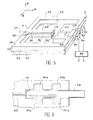
- FIG. 5 represents a device capable of implementing optical fiber positioning structures according to the invention.
- the device shown is an optomechanical device. It comprises a planar layer, or guide structure 50 (which may be composed of one or more layers), which is produced on a substrate 52, for example made of monocrystalline silicon, and which has an entry face E and a face of parallel S outputs, obtained for example by cleavage.
- the guide structure 50 comprises for example a buffer layer 54 made of silicon oxide (8 to 12 ⁇ m thick), and an upper layer 56 made of silica (2 to 10 ⁇ m thick), the latter being able, for certain applications, to be replaced by air.
- the guide structure also includes an input microguide 58 and two output microguides 60 and 62, made of silicon oxide doped for example with phosphorus, from 2 to 6 ⁇ m in height and from 2 to 8 ⁇ m in width as well as a multimode coupler 64 having substantially the same height (from 2 ⁇ m to 6 ⁇ m), for a width typically between 10 ⁇ m and 50 ⁇ m.
- the microguides 58, 60, 62 are parallel to a direction x, itself parallel to the largest surface 59 of the planar layer or guide structure 50, and they are arranged on either side of a recess 66 crossing the guide structure 50.
- the recess 66 defines, in the guiding structure 50 and the substrate a fixed part, a flexible beam 68 oriented at rest parallel to the direction x, this beam being able to move in the recess 66 in a direction y, parallel to the surface 59 of the guide structure and perpendicular to the direction x.
- This beam 68 includes a fixed end 70, integral with the fixed part, and a free end 72 able to move in the recess 66.
- a central microguide 74 extends over the entire length of the beam 68, its end 76 opening out at the end 72 thereof.
- the multimode coupler 64 is placed opposite the end 76 of the microguide 74.
- the term “multimode coupler” is understood to mean a multimode coupler or guide having several propagation modes or several single-mode guides.
- the length L of the multimode coupler 64 is preferably such that, when an incident beam I directed on the input section of the coupler has an intensity distribution comprising a single maximum, an output beam is obtained having a number N maximum, with N ⁇ 2.
- An optical signal is produced by a radiation source (for example at the wavelength 0.78 ⁇ m) not shown in FIG. 5, then is transmitted by an input optical fiber 57 and by the microguide 58 then 74 in direction of the multimode coupler 64.
- Each output microguide is positioned at the location of a maximum, at the output of the coupler, when the input beam is in position centered on the input of the coupler.
- Each detector delivers a signal representative of the optical signal transmitted by the optical fiber at the output of which it is arranged. Finally, these detectors are connected to means 86 for processing the signals which they deliver.
- the free end of the beam 68 moves in the direction y, which modifies the distribution of the radiation at the output of the multimode coupler, therefore of the radiation transmitted by the N output guides 60, 62 , and therefore the signal produced by the detectors 82, 84.
- connection zones thus defined correspond to the groove capable of receiving the optical fibers.
- the connection area 90 provided for the fiber 78 can also be widened in certain places 90a, 90b, 90c , 90d in accordance with the present invention, to facilitate the supply of optical adhesive and allow the fibers to be held in place.
- the widenings 90a-90d are made at the same time as the connection area 90. This can be applied to the connection zone of each of the fibers 57, 78, 80.
Landscapes
- Physics & Mathematics (AREA)
- General Physics & Mathematics (AREA)
- Optics & Photonics (AREA)
- Engineering & Computer Science (AREA)
- Microelectronics & Electronic Packaging (AREA)
- Mechanical Coupling Of Light Guides (AREA)
- Optical Couplings Of Light Guides (AREA)
Applications Claiming Priority (2)
| Application Number | Priority Date | Filing Date | Title |
|---|---|---|---|
| FR9605841A FR2748574B1 (fr) | 1996-05-10 | 1996-05-10 | Procede et dispositif pour le positionnement et le maintien de fibres optiques |
| FR9605841 | 1996-05-10 |
Publications (2)
| Publication Number | Publication Date |
|---|---|
| EP0806686A1 true EP0806686A1 (de) | 1997-11-12 |
| EP0806686B1 EP0806686B1 (de) | 2006-11-02 |
Family
ID=9492016
Family Applications (1)
| Application Number | Title | Priority Date | Filing Date |
|---|---|---|---|
| EP97401031A Expired - Lifetime EP0806686B1 (de) | 1996-05-10 | 1997-05-07 | Verfahren und Vorrichtung zum Ausrichten und Fixieren von optischen Fasern |
Country Status (5)
| Country | Link |
|---|---|
| US (1) | US5937132A (de) |
| EP (1) | EP0806686B1 (de) |
| JP (1) | JPH1048454A (de) |
| DE (1) | DE69736874T2 (de) |
| FR (1) | FR2748574B1 (de) |
Families Citing this family (9)
| Publication number | Priority date | Publication date | Assignee | Title |
|---|---|---|---|---|
| JP3463273B2 (ja) | 1999-11-24 | 2003-11-05 | 勝治 安藤 | 水洗トイレのロータンク |
| EP1186920A1 (de) | 2000-09-08 | 2002-03-13 | Corning Incorporated | Werkzeug und Verfahren zur Positionierung von optischen Fasermatrixen |
| US20020094185A1 (en) * | 2000-12-12 | 2002-07-18 | Ian Hopkin | Holding a component on an optical micro bench |
| US6440776B1 (en) | 2000-12-12 | 2002-08-27 | Jds Uniphase Inc. | Securing an optical component onto a micro bench |
| KR20050021055A (ko) * | 2003-08-26 | 2005-03-07 | 삼성에스디아이 주식회사 | 플라즈마 디스플레이 패널 |
| JP4776464B2 (ja) * | 2006-07-24 | 2011-09-21 | 古河電気工業株式会社 | 光デバイスの製造方法 |
| JP5115774B2 (ja) * | 2011-04-18 | 2013-01-09 | Necエンジニアリング株式会社 | 光ファイバ用クランプ構造 |
| US10739517B2 (en) * | 2018-09-21 | 2020-08-11 | Ofs Fitel, Llc | Cleaving optical fibers |
| DE102021102869B4 (de) | 2021-02-08 | 2022-11-10 | Deutsches Zentrum für Luft- und Raumfahrt e.V. | Verfahren zum Ausrichten von optischen Fasern und Vorrichtungen zur Verwendung bei den Verfahren |
Citations (7)
| Publication number | Priority date | Publication date | Assignee | Title |
|---|---|---|---|---|
| US4183616A (en) * | 1976-07-20 | 1980-01-15 | Societe D'exploitation Des Cables Electriques | Connector for connecting two groups of optical fibres |
| JPS5565913A (en) * | 1978-11-13 | 1980-05-17 | Nippon Telegr & Teleph Corp <Ntt> | Optical fiber multicore connecting method and connector |
| JPS6086514A (ja) * | 1983-10-18 | 1985-05-16 | Nippon Telegr & Teleph Corp <Ntt> | 光フアイバの接続法 |
| WO1987000298A1 (en) * | 1985-07-10 | 1987-01-15 | Plessey Overseas Limited | Methods of positioning an optical fibre |
| JPH03233412A (ja) * | 1990-02-08 | 1991-10-17 | Nec Corp | 光接続方法及びレーザエッチング加工方法 |
| JPH07151929A (ja) * | 1993-11-29 | 1995-06-16 | Hitachi Cable Ltd | ファイバアレイ |
| US5506928A (en) * | 1995-05-30 | 1996-04-09 | Ats Automation Tooling Systems Inc. | Optical fiber gripping and positioning apparatus |
Family Cites Families (1)
| Publication number | Priority date | Publication date | Assignee | Title |
|---|---|---|---|---|
| FR2659148B1 (fr) * | 1990-03-01 | 1993-04-16 | Commissariat Energie Atomique | Procede de connexion entre une fibre optique et un microguide optique. |
-
1996
- 1996-05-10 FR FR9605841A patent/FR2748574B1/fr not_active Expired - Fee Related
-
1997
- 1997-04-29 US US08/848,280 patent/US5937132A/en not_active Expired - Lifetime
- 1997-05-07 DE DE69736874T patent/DE69736874T2/de not_active Expired - Lifetime
- 1997-05-07 EP EP97401031A patent/EP0806686B1/de not_active Expired - Lifetime
- 1997-05-09 JP JP9119900A patent/JPH1048454A/ja not_active Withdrawn
Patent Citations (7)
| Publication number | Priority date | Publication date | Assignee | Title |
|---|---|---|---|---|
| US4183616A (en) * | 1976-07-20 | 1980-01-15 | Societe D'exploitation Des Cables Electriques | Connector for connecting two groups of optical fibres |
| JPS5565913A (en) * | 1978-11-13 | 1980-05-17 | Nippon Telegr & Teleph Corp <Ntt> | Optical fiber multicore connecting method and connector |
| JPS6086514A (ja) * | 1983-10-18 | 1985-05-16 | Nippon Telegr & Teleph Corp <Ntt> | 光フアイバの接続法 |
| WO1987000298A1 (en) * | 1985-07-10 | 1987-01-15 | Plessey Overseas Limited | Methods of positioning an optical fibre |
| JPH03233412A (ja) * | 1990-02-08 | 1991-10-17 | Nec Corp | 光接続方法及びレーザエッチング加工方法 |
| JPH07151929A (ja) * | 1993-11-29 | 1995-06-16 | Hitachi Cable Ltd | ファイバアレイ |
| US5506928A (en) * | 1995-05-30 | 1996-04-09 | Ats Automation Tooling Systems Inc. | Optical fiber gripping and positioning apparatus |
Non-Patent Citations (4)
| Title |
|---|
| PATENT ABSTRACTS OF JAPAN vol. 004, no. 107 (P - 021) 31 July 1980 (1980-07-31) * |
| PATENT ABSTRACTS OF JAPAN vol. 009, no. 232 (P - 389) 18 September 1985 (1985-09-18) * |
| PATENT ABSTRACTS OF JAPAN vol. 016, no. 015 (P - 1298) 14 January 1992 (1992-01-14) * |
| PATENT ABSTRACTS OF JAPAN vol. 95, no. 009 31 October 1995 (1995-10-31) * |
Also Published As
| Publication number | Publication date |
|---|---|
| EP0806686B1 (de) | 2006-11-02 |
| JPH1048454A (ja) | 1998-02-20 |
| FR2748574A1 (fr) | 1997-11-14 |
| FR2748574B1 (fr) | 1998-05-29 |
| DE69736874D1 (de) | 2006-12-14 |
| US5937132A (en) | 1999-08-10 |
| DE69736874T2 (de) | 2007-05-24 |
Similar Documents
| Publication | Publication Date | Title |
|---|---|---|
| EP0637764B1 (de) | Herstellung einer optischen Kopplungsstruktur, die einen abgespaltenen optischen Wellenleiter und eine Halterung für optische Fasern integriert | |
| EP0471066B1 (de) | Verbindungsmethoden zwischen einer optischen faser und einem optischen wellenleiter | |
| EP1269238B1 (de) | Verfahren und vorrichtung für optische fasern und optoelektronische bauelemente passiver ausrichtung | |
| FR3066615B1 (fr) | Puce photonique a structure de collimation integree | |
| EP0603042A1 (de) | Monolithisches System zur Kopplung zwischen einer optischen Faser und optoelektronischem Bauteil | |
| EP1048964A1 (de) | Zusammenbau einer Chipintegrierten optischen Schaltung zur Herstellung eines miniaturisierten optisches Bauelementes | |
| FR2752623A1 (fr) | Procede de fabrication d'un dispositif de couplage optique collectif et dispositif obtenu par un tel procede | |
| EP2216663B1 (de) | Struktur und Verfahren zur Justierung einer optischen Faser mit einem sub-mikronischen Lichtwellenleiter | |
| EP0806686B1 (de) | Verfahren und Vorrichtung zum Ausrichten und Fixieren von optischen Fasern | |
| EP0069054A2 (de) | Vorrichtung zur Verbindung von optischen Fasern und Verfahren zu ihrer Herstellung | |
| EP3538937B1 (de) | Verfahren zur gemeinsamen herstellung einer vielzahl von optoelektronischen chips | |
| EP0863417A1 (de) | Integrierte Multiplex-Verzweigvorrichtung für Mehrkernfasern | |
| EP0677758B1 (de) | Optische Anordnung zum Koppeln einer optischen Faser mit einem kreisförmigen Modenfeld und eines optoelektronischen Wandlers mit einem elliptischen Modenfeld sowie deren Herstellungsverfahren | |
| FR2773222A1 (fr) | Structure pour connecter des fibres optiques a un guide d'onde optique | |
| FR2823859A1 (fr) | Support de positionnement et de maintien de fibres optiques et son procede de realisation | |
| EP0587496A1 (de) | Verfahren zur Vorbereitung einer Verbindung und Verfahren zum Verbinden durch Spleissen von einer integrierten optischen Vorrichtung mit einem optischen Kabel und Verbindungsuntereinheiten zur Ausführung des Verfahrens | |
| EP0190962B1 (de) | Vorrichtung für faseroptische Kupplung und Verfahren zu deren Herstellung | |
| EP1433232B1 (de) | Wellenleiterlaserquelle | |
| EP1621906B1 (de) | Vorrichtung mit bündig montiertem optelektronischem Element das von einem Lichtwellenleiter bedeckt ist | |
| FR2817975A1 (fr) | Procede et dispositif d'alignement passif de fibres optiques et de composants, utilisant des entailles en croix | |
| CH639497A5 (fr) | Procede de realisation d'un coupleur directionnel de fibres optiques et jonction-etoile obtenue par ce procede. | |
| FR2816064A1 (fr) | Procede de realisation d'un guide d'onde, notamment optique, et dispositif de couplage optique comportant un tel guide | |
| FR2815139A1 (fr) | Procede et dispositif d'alignement passif d'un connecteur optique multifibres et d'un composant optique | |
| FR2830628A1 (fr) | Support de positionnement et de maintien de fibres optiques et procede de realisation d'un tel support | |
| WO2007028911A1 (fr) | Couplage optique |
Legal Events
| Date | Code | Title | Description |
|---|---|---|---|
| PUAI | Public reference made under article 153(3) epc to a published international application that has entered the european phase |
Free format text: ORIGINAL CODE: 0009012 |
|
| AK | Designated contracting states |
Kind code of ref document: A1 Designated state(s): CH DE FR GB IT LI |
|
| 17P | Request for examination filed |
Effective date: 19980417 |
|
| 17Q | First examination report despatched |
Effective date: 20050302 |
|
| GRAP | Despatch of communication of intention to grant a patent |
Free format text: ORIGINAL CODE: EPIDOSNIGR1 |
|
| GRAS | Grant fee paid |
Free format text: ORIGINAL CODE: EPIDOSNIGR3 |
|
| GRAA | (expected) grant |
Free format text: ORIGINAL CODE: 0009210 |
|
| AK | Designated contracting states |
Kind code of ref document: B1 Designated state(s): CH DE FR GB IT LI |
|
| PG25 | Lapsed in a contracting state [announced via postgrant information from national office to epo] |
Ref country code: IT Free format text: LAPSE BECAUSE OF FAILURE TO SUBMIT A TRANSLATION OF THE DESCRIPTION OR TO PAY THE FEE WITHIN THE PRE;WARNING: LAPSES OF ITALIAN PATENTS WITH EFFECTIVE DATE BEFORE 2007 MAY HAVE OCCURRED AT ANY TIME BEFORE 2007. THE CORRECT EFFECTIVE DATE MAY BE DIFFERENT FROM THE ONE RECORDED.SCRIBED TIME-LIMIT Effective date: 20061102 |
|
| RAP1 | Party data changed (applicant data changed or rights of an application transferred) |
Owner name: COMMISSARIAT A L'ENERGIE ATOMIQUE |
|
| REG | Reference to a national code |
Ref country code: GB Ref legal event code: FG4D Free format text: NOT ENGLISH |
|
| REG | Reference to a national code |
Ref country code: CH Ref legal event code: EP |
|
| REF | Corresponds to: |
Ref document number: 69736874 Country of ref document: DE Date of ref document: 20061214 Kind code of ref document: P |
|
| GBT | Gb: translation of ep patent filed (gb section 77(6)(a)/1977) |
Effective date: 20070111 |
|
| PLBE | No opposition filed within time limit |
Free format text: ORIGINAL CODE: 0009261 |
|
| STAA | Information on the status of an ep patent application or granted ep patent |
Free format text: STATUS: NO OPPOSITION FILED WITHIN TIME LIMIT |
|
| 26N | No opposition filed |
Effective date: 20070803 |
|
| PGFP | Annual fee paid to national office [announced via postgrant information from national office to epo] |
Ref country code: CH Payment date: 20110524 Year of fee payment: 15 |
|
| REG | Reference to a national code |
Ref country code: CH Ref legal event code: PL |
|
| PG25 | Lapsed in a contracting state [announced via postgrant information from national office to epo] |
Ref country code: LI Free format text: LAPSE BECAUSE OF NON-PAYMENT OF DUE FEES Effective date: 20120531 Ref country code: CH Free format text: LAPSE BECAUSE OF NON-PAYMENT OF DUE FEES Effective date: 20120531 |
|
| PGFP | Annual fee paid to national office [announced via postgrant information from national office to epo] |
Ref country code: IT Payment date: 20130513 Year of fee payment: 17 |
|
| PGFP | Annual fee paid to national office [announced via postgrant information from national office to epo] |
Ref country code: GB Payment date: 20140520 Year of fee payment: 18 |
|
| PGFP | Annual fee paid to national office [announced via postgrant information from national office to epo] |
Ref country code: DE Payment date: 20140509 Year of fee payment: 18 |
|
| PGFP | Annual fee paid to national office [announced via postgrant information from national office to epo] |
Ref country code: FR Payment date: 20140602 Year of fee payment: 18 |
|
| PG25 | Lapsed in a contracting state [announced via postgrant information from national office to epo] |
Ref country code: IT Free format text: LAPSE BECAUSE OF NON-PAYMENT OF DUE FEES Effective date: 20140507 |
|
| REG | Reference to a national code |
Ref country code: DE Ref legal event code: R119 Ref document number: 69736874 Country of ref document: DE |
|
| GBPC | Gb: european patent ceased through non-payment of renewal fee |
Effective date: 20150507 |
|
| REG | Reference to a national code |
Ref country code: FR Ref legal event code: ST Effective date: 20160129 |
|
| PG25 | Lapsed in a contracting state [announced via postgrant information from national office to epo] |
Ref country code: DE Free format text: LAPSE BECAUSE OF NON-PAYMENT OF DUE FEES Effective date: 20151201 Ref country code: GB Free format text: LAPSE BECAUSE OF NON-PAYMENT OF DUE FEES Effective date: 20150507 |
|
| PG25 | Lapsed in a contracting state [announced via postgrant information from national office to epo] |
Ref country code: FR Free format text: LAPSE BECAUSE OF NON-PAYMENT OF DUE FEES Effective date: 20150601 |