EP0806658A1 - Méthode pour détecter des fissures dans des substrats en céramique - Google Patents
Méthode pour détecter des fissures dans des substrats en céramique Download PDFInfo
- Publication number
- EP0806658A1 EP0806658A1 EP97303089A EP97303089A EP0806658A1 EP 0806658 A1 EP0806658 A1 EP 0806658A1 EP 97303089 A EP97303089 A EP 97303089A EP 97303089 A EP97303089 A EP 97303089A EP 0806658 A1 EP0806658 A1 EP 0806658A1
- Authority
- EP
- European Patent Office
- Prior art keywords
- ceramic substrate
- crack
- conductive liquid
- conductors
- insulation resistance
- Prior art date
- Legal status (The legal status is an assumption and is not a legal conclusion. Google has not performed a legal analysis and makes no representation as to the accuracy of the status listed.)
- Granted
Links
Images


Classifications
-
- G—PHYSICS
- G01—MEASURING; TESTING
- G01N—INVESTIGATING OR ANALYSING MATERIALS BY DETERMINING THEIR CHEMICAL OR PHYSICAL PROPERTIES
- G01N27/00—Investigating or analysing materials by the use of electric, electrochemical, or magnetic means
- G01N27/02—Investigating or analysing materials by the use of electric, electrochemical, or magnetic means by investigating impedance
- G01N27/04—Investigating or analysing materials by the use of electric, electrochemical, or magnetic means by investigating impedance by investigating resistance
- G01N27/20—Investigating the presence of flaws
- G01N27/205—Investigating the presence of flaws in insulating materials
Definitions
- the present invention relates to a method of inspecting for cracks in a ceramic substrate, and in particular, a ceramic substrate used in manufacturing a sensor, a resistor element, an actuator for an ink-jet print head, etc.
- a ceramic substrate coated with a conductive film has been used as an electrode, a resistor, a lead, an output terminal, etc. in a sensor, a resistor element, an actuator for an ink-jet print head, etc.
- a method of applying by printing conductive paste on a ceramic substrate is appropriate. It is because a uniform film having a complicated pattern can be efficiently formed and the conductive film can be adjusted to have a wide range of thickness by adjusting the viscosity of the conductive paste.
- a red check test As a method of inspecting any crack in a ceramic substrate, conventionally, there are known a red check test, a method of inspection by visual observation or with microscope using liquid penetrant (liquid penetrant test) such as a fluorescent penetrant test, a method of inspection by detecting leakage of gas such as gaseous helium and air, a method using an image processor, etc.
- the liquid penetrant test suffers from a problem that it depends to a great extent on the skillfulness of the inspector, cracks are likely to be left undetected, and the result of the inspection is difficult to express as numerical data. Further, in case a ceramic substrate applied to, for example, an actuator for an ink-jet print head has a multilayer functional film formed thereon, there is a problem that, according to the method using liquid penetrant, it takes the liquid penetrant much time to ooze.
- the method of inspection by detecting leakage of gas has a problem that, since closed space is necessary, there is technical difficulty and the scale of the apparatus has to be large.
- the method using an image processor has a problem that, depending on the resolution of the apparatus, a microscopic crack may be difficult to detect.
- an object of the present invention is to provide a method of inspecting for cracks in a ceramic substrate which reduces or eliminates the inconveniences mentioned above, and for example detects even a crack that is not exposed on the surface of a ceramic substrate, does not leave a crack undetected, and can make objective judgement possible by expressing the result of inspection, as numerical data.
- a method of inspecting any crack in a ceramic substrate which comprises; disposing conductors on both faces of the ceramic substrate, both of the conductors being conductive liquid, and measuring an insulation resistance value between both faces of the ceramic substrate or an electrically characteristic value which depends on the insulation resistance value with the conductive liquid or other conductors electrically connected to the conductive liquid being as electrodes.
- a method of inspecting any crack in a ceramic substrate which comprises; disposing conductors on both faces of the ceramic substrate, one of the conductors being conductive liquid and the other of the conductors having a plane electrically connected portion or other shape conforming to the face of the substrate, and measuring an insulation resistance value between both faces of the ceramic substrate or an electrically characteristic value which depends on the insulation resistance value with the conductor having the plane electrically connected portion or other shapes and the conductive liquid or another conductor electrically connected to the conductive liquid being as electrodes.
- a method of inspecting any crack in a ceramic substrate including a conductive film at least on one face which comprises; disposing conductive liquid on the other face of the ceramic substrate, and measuring an insulation resistance value between both faces of the ceramic substrate or an electrically characteristic value which depends on the insulation resistance value with the conductive film and the conductive liquid or another conductor electrically connected to the conductive liquid being as electrodes.
- the other conductor may be the whole or a part of a container containing the conductive liquid. Still further, the electrically characteristic value may be dielectric loss.
- a crack in the ceramic substrate is detected.
- conductive liquid is used as at least one of the conductors.
- the principle of the method of the present invention as mentioned in the above requires that at least a conductor on one face of the ceramic substrate is the liquid, but the conductor on the other face of the ceramic substrate is not necessarily required to be the liquid.
- the conductor disposed on the other face has a plane electrically connected portion which can be in close contact with the face of the ceramic substrate.
- a plane conductor having an area and a shape substantially similar to those of the ceramic substrate is used.
- a plastic material is used as the conductor, it can also be applied to inspection of a bent ceramic substrate.
- the conductive film can be used as an electrode.
- one of the electrodes is a conductive film provided on one face of the ceramic substrate while the other of the electrodes is a conductor formed of the conductive liquid disposed on the other face of the ceramic substrate.
- another conductor electrically connected to the conductive liquid may be used as an electrode.
- the whole or a part of a container containing the conductive liquid may be formed of a conductive material such that the container or the conductive portion of the container is used as an electrode.
- the specific resistivity of the conductive liquid used in the present invention is small.
- the specific resistivity is preferably 0-20 ⁇ ⁇ m, and is, more preferably, 0 - 2 ⁇ ⁇ m.
- the surface tension of the conductive liquid is small.
- the surface tension is preferably 0 - 80 dyn/cm, and is, more preferably, 0 - 50 dyn/cm. If the surface tension is more than 80 dyn/cm, the wettability is so small that the capillary phenomenon is difficult to occur, thereby lowering the precision of detecting a crack.
- the viscosity of the conductive liquid is preferable 0 - 1,000 mPa ⁇ s, and is, more preferably, 1 - 300 mPa ⁇ s. If the viscosity is more than 1,000 mPa ⁇ s, the fluidity of the liquid is so small that bubbles are likely to be contained therein.
- the conductive liquid has a high washability and a low foamability. Further, a small amount of a defoaming agent such as alcohol may be added to the conductive liquid optionally. If the conductive liquid has a low washability, a component of the liquid may remain on the ceramic substrate, causing a stain or defective insulation. If the conductive liquid has a high foamability, bubbles between the conductive liquid and the ceramic substrate makes the electric resistance large, thereby increasing noise in the measurement.
- a defoaming agent such as alcohol
- the conductive liquid used in the present invention synthetic detergent, conductive coating, etc. are preferable, and in particular, synthetic detergent having a low foamability is preferable.
- the conductive liquid As the other materials electrically connected to the conductive liquid and, in case the conductive liquid is used only on one side of a ceramic substrate, as a material for the conductor disposed on the opposite side to the conductive liquid, Au, Ag, Pt, Cu, Al, SUS, etc. are used. Preferably, a material having a small specific resistivity is used.
- the measured voltage when the dielectric loss is measured is in the range to which an ordinary LCR meter can be set, that is, from 5 mV to 2 V, around 1.0 V which is popularly used is sufficient.
- the measured frequency is preferably 100 Hz - 100 kHz, and more preferably, 300 Hz - 1 kHz.
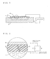
- Fig. 1 shows an inspection apparatus used in the measurement.
- Fig. 2 is an enlarged view of a part shown in Fig. 1.
- a ceramic substrate 3 is mounted on a container 2 formed of a conductive metal filled with conductive liquid 1 such that a face of the ceramic substrate 3 which does not have a conductive film 4 is in contact with the liquid 1.
- the conductive film 4 and the container 2 are connected to an LCR meter via leads 6.
- the inspection was made by measuring dielectric loss under the following conditions: the measured voltage was 1 V; the measured frequency was 1 kHz, the bias voltage was 0 V; and the specific resistivity, the wettability expressed as the surface tension, and the viscosity of the conductive liquid 1 were 1.0 ⁇ ⁇ m, 28.0 dyn/cm, and 50 mPa ⁇ s, respectively.
- Fig. 3 shows the results of the measurement in the inspection of the ceramic substrates for a crack.
- results of inspection according to the liquid penetrant test are put in parentheses in Fig. 3.
- "OK” means that the judgement was that there is no crack
- "NG” means that the judgement was that there is a crack.
- Fig. 4 shows another example of an inspection apparatus used in the method of inspection for a crack according to the present invention.
- the ceramic substrate 3 is connected in series to a reference resistance R ref .
- Voltage V c of the ceramic substrate 3 when constant voltage V s is applied is measured.
Landscapes
- Chemical & Material Sciences (AREA)
- Chemical Kinetics & Catalysis (AREA)
- Electrochemistry (AREA)
- Physics & Mathematics (AREA)
- Health & Medical Sciences (AREA)
- Life Sciences & Earth Sciences (AREA)
- Analytical Chemistry (AREA)
- Biochemistry (AREA)
- General Health & Medical Sciences (AREA)
- General Physics & Mathematics (AREA)
- Immunology (AREA)
- Pathology (AREA)
- Investigating Or Analyzing Materials By The Use Of Electric Means (AREA)
Applications Claiming Priority (3)
| Application Number | Priority Date | Filing Date | Title |
|---|---|---|---|
| JP11461196 | 1996-05-09 | ||
| JP114611/96 | 1996-05-09 | ||
| JP11461196A JP3569072B2 (ja) | 1996-05-09 | 1996-05-09 | セラミック基板のクラック検査方法 |
Publications (2)
| Publication Number | Publication Date |
|---|---|
| EP0806658A1 true EP0806658A1 (fr) | 1997-11-12 |
| EP0806658B1 EP0806658B1 (fr) | 2005-02-09 |
Family
ID=14642198
Family Applications (1)
| Application Number | Title | Priority Date | Filing Date |
|---|---|---|---|
| EP97303089A Expired - Lifetime EP0806658B1 (fr) | 1996-05-09 | 1997-05-07 | Méthode pour détecter des fissures dans des substrats en céramique |
Country Status (4)
| Country | Link |
|---|---|
| US (1) | US5969532A (fr) |
| EP (1) | EP0806658B1 (fr) |
| JP (1) | JP3569072B2 (fr) |
| DE (1) | DE69732445T2 (fr) |
Cited By (5)
| Publication number | Priority date | Publication date | Assignee | Title |
|---|---|---|---|---|
| EP1816470A1 (fr) * | 2006-02-03 | 2007-08-08 | Ngk Insulators, Ltd. | Procédé d'inspection d'un assemblage stratifié et procédé d'inspection d'un module dissipateur thermique |
| RU2446392C1 (ru) * | 2010-11-24 | 2012-03-27 | Открытое акционерное общество Таганрогский авиационный научно-технический комплекс им. Г.М. Бериева | Способ установки датчиков обнаружения трещин |
| CN109142470A (zh) * | 2018-09-29 | 2019-01-04 | 业成科技(成都)有限公司 | 侦测装置及识别系统 |
| US11112626B2 (en) * | 2017-01-27 | 2021-09-07 | Merck Patent Gmbh | Method for detecting breakage of substrate of a switchable optical element and switchable optical device |
| CN113625129A (zh) * | 2021-07-22 | 2021-11-09 | 西安交通大学 | 一种基于等效电容的dbc基板界面裂纹发展状态评估方法 |
Families Citing this family (19)
| Publication number | Priority date | Publication date | Assignee | Title |
|---|---|---|---|---|
| US6411110B1 (en) * | 1999-08-17 | 2002-06-25 | Micron Technology, Inc. | Apparatuses and methods for determining if protective coatings on semiconductor substrate holding devices have been compromised |
| JP3867666B2 (ja) * | 2002-12-13 | 2007-01-10 | 株式会社デンソー | 積層型ガスセンサ素子の検査方法 |
| FR2850459B1 (fr) * | 2003-01-29 | 2005-06-24 | Pass Technologies | Dispositif de surveillance de l'integrite du contact d'un joint |
| US7180302B2 (en) | 2004-07-16 | 2007-02-20 | Simula, Inc | Method and system for determining cracks and broken components in armor |
| JP2006038988A (ja) * | 2004-07-23 | 2006-02-09 | Seiko Epson Corp | 電気光学装置、電子機器、および実装構造体 |
| JP4974936B2 (ja) * | 2008-03-05 | 2012-07-11 | 日本特殊陶業株式会社 | ガスセンサ素子の検査方法 |
| JP5489968B2 (ja) * | 2010-12-09 | 2014-05-14 | 日本発條株式会社 | 圧電素子のクラック検出方法及びその装置 |
| JP5839986B2 (ja) * | 2011-12-26 | 2016-01-06 | 日産自動車株式会社 | 検査方法および検査システム |
| JP5989471B2 (ja) * | 2012-09-14 | 2016-09-07 | 日本発條株式会社 | 圧電素子供給方法 |
| KR102043179B1 (ko) * | 2013-02-18 | 2019-11-12 | 삼성디스플레이 주식회사 | 배리어 막의 결함 검출 방법 및 배리어 막의 결함 검출 장치 |
| KR101448518B1 (ko) * | 2013-04-18 | 2014-10-10 | 현대오트론 주식회사 | 차량용 ecu 제조 방법 및 그 장치 |
| JP6540593B2 (ja) * | 2016-05-11 | 2019-07-10 | 株式会社デンソー | 欠陥検査装置、および、欠陥検査方法 |
| WO2018093895A1 (fr) * | 2016-11-16 | 2018-05-24 | 3M Innovative Properties Company | Suppression de tensions induites thermiquement pour vérifier l'intégrité structurale de matériaux |
| CN108061209A (zh) * | 2017-10-30 | 2018-05-22 | 江阴市恒润环锻有限公司 | 一种可用于法兰外圆裂纹监测的法兰 |
| DE102018111998A1 (de) * | 2018-05-18 | 2019-11-21 | Mack Rides Gmbh & Co. Kg | Sensorik zur frühzeitigen Erkennung physikalischer Veränderungen |
| DE102018210613A1 (de) | 2018-06-28 | 2020-01-02 | Robert Bosch Gmbh | Kontaktsystem mit einer Risserfassungsvorrichtung |
| CN108828071A (zh) * | 2018-07-05 | 2018-11-16 | 江苏德意高航空智能装备股份有限公司 | 着色和荧光两用探伤显像纸巾及纸巾显像应用 |
| US20210293645A1 (en) * | 2020-03-17 | 2021-09-23 | Arris Enterprises Llc | Ceramic based strain detector |
| CN115078480A (zh) * | 2022-06-24 | 2022-09-20 | 东莞市仙桥电子科技有限公司 | 一种ntc锭子烧结微裂纹的快速检验方法 |
Citations (5)
| Publication number | Priority date | Publication date | Assignee | Title |
|---|---|---|---|---|
| FR2304078A1 (fr) * | 1975-03-12 | 1976-10-08 | Goeppner Kaiserslautern Eisen | Procede de detection de nouveaux defauts apparaissant dans des revetements de recipients |
| GB2034898A (en) * | 1978-10-23 | 1980-06-11 | Pecorara G | Device for detecting discontinuities in the structure of ceramic floor tiles |
| JPS58111749A (ja) * | 1981-12-25 | 1983-07-02 | Fuji Ratetsukusu Kk | コンド−ムのピンホ−ルの検査方法 |
| FR2607254A1 (fr) * | 1986-11-25 | 1988-05-27 | Centre Nat Rech Scient | Procede et dispositif de caracterisation d'un film de polymere et application aux films a usage electrique |
| JPH07161570A (ja) * | 1993-12-09 | 1995-06-23 | Murata Mfg Co Ltd | 積層セラミックコンデンサの内部クラック検出方法 |
Family Cites Families (5)
| Publication number | Priority date | Publication date | Assignee | Title |
|---|---|---|---|---|
| US3803485A (en) * | 1970-02-16 | 1974-04-09 | Battelle Development Corp | Indicating coating for locating fatigue cracks |
| US4503710A (en) * | 1983-06-08 | 1985-03-12 | Conoco Inc. | Crack detection by electrical resistance |
| JPS63177051A (ja) * | 1987-01-19 | 1988-07-21 | Nec Corp | 絶縁層のピンホ−ル検出方法 |
| JP2531891B2 (ja) * | 1991-03-20 | 1996-09-04 | 日本碍子株式会社 | セラミック体の欠陥検出方法 |
| US5378991A (en) * | 1992-05-27 | 1995-01-03 | Anderson; Thomas F. | Detecting degradation of non-conductive inert wall layers in fluid containers |
-
1996
- 1996-05-09 JP JP11461196A patent/JP3569072B2/ja not_active Expired - Lifetime
-
1997
- 1997-04-30 US US08/841,105 patent/US5969532A/en not_active Expired - Lifetime
- 1997-05-07 EP EP97303089A patent/EP0806658B1/fr not_active Expired - Lifetime
- 1997-05-07 DE DE69732445T patent/DE69732445T2/de not_active Expired - Lifetime
Patent Citations (5)
| Publication number | Priority date | Publication date | Assignee | Title |
|---|---|---|---|---|
| FR2304078A1 (fr) * | 1975-03-12 | 1976-10-08 | Goeppner Kaiserslautern Eisen | Procede de detection de nouveaux defauts apparaissant dans des revetements de recipients |
| GB2034898A (en) * | 1978-10-23 | 1980-06-11 | Pecorara G | Device for detecting discontinuities in the structure of ceramic floor tiles |
| JPS58111749A (ja) * | 1981-12-25 | 1983-07-02 | Fuji Ratetsukusu Kk | コンド−ムのピンホ−ルの検査方法 |
| FR2607254A1 (fr) * | 1986-11-25 | 1988-05-27 | Centre Nat Rech Scient | Procede et dispositif de caracterisation d'un film de polymere et application aux films a usage electrique |
| JPH07161570A (ja) * | 1993-12-09 | 1995-06-23 | Murata Mfg Co Ltd | 積層セラミックコンデンサの内部クラック検出方法 |
Non-Patent Citations (3)
| Title |
|---|
| ANONIMOUS: "SPONGE PROBE PINPOINTS PINHOLES", MACHINE DESIGN, vol. 53, no. 15, 1981, CLEVELAND US, pages 40, XP002038073 * |
| PATENT ABSTRACTS OF JAPAN vol. 095, no. 009 31 October 1995 (1995-10-31) * |
| PATENT ABSTRACTS OF JAPAN vol. 7, no. 220 (P - 226)<1365> 30 September 1983 (1983-09-30) * |
Cited By (5)
| Publication number | Priority date | Publication date | Assignee | Title |
|---|---|---|---|---|
| EP1816470A1 (fr) * | 2006-02-03 | 2007-08-08 | Ngk Insulators, Ltd. | Procédé d'inspection d'un assemblage stratifié et procédé d'inspection d'un module dissipateur thermique |
| RU2446392C1 (ru) * | 2010-11-24 | 2012-03-27 | Открытое акционерное общество Таганрогский авиационный научно-технический комплекс им. Г.М. Бериева | Способ установки датчиков обнаружения трещин |
| US11112626B2 (en) * | 2017-01-27 | 2021-09-07 | Merck Patent Gmbh | Method for detecting breakage of substrate of a switchable optical element and switchable optical device |
| CN109142470A (zh) * | 2018-09-29 | 2019-01-04 | 业成科技(成都)有限公司 | 侦测装置及识别系统 |
| CN113625129A (zh) * | 2021-07-22 | 2021-11-09 | 西安交通大学 | 一种基于等效电容的dbc基板界面裂纹发展状态评估方法 |
Also Published As
| Publication number | Publication date |
|---|---|
| EP0806658B1 (fr) | 2005-02-09 |
| JPH09304324A (ja) | 1997-11-28 |
| DE69732445D1 (de) | 2005-03-17 |
| DE69732445T2 (de) | 2006-04-27 |
| US5969532A (en) | 1999-10-19 |
| JP3569072B2 (ja) | 2004-09-22 |
Similar Documents
| Publication | Publication Date | Title |
|---|---|---|
| US5969532A (en) | Method of inspecting crack in ceramic substrate | |
| US7429865B2 (en) | Method and system for error checking an electrochemical sensor | |
| US4549134A (en) | Moisture probe and technique | |
| US7378852B2 (en) | Measuring device having a plurality of potentiometric electrode pairs situated on a substrate | |
| EP0587665B1 (fr) | Electro-analyse de liquides et elements de detection a utiliser pour ladite analyse | |
| US4455212A (en) | Gel electrode for early detection of metal fatigue | |
| US3419479A (en) | Anodic printing for detecting defective sites in valve metal oxide films | |
| US2962426A (en) | Electrochemical method for analyzing materials | |
| CN114184689A (zh) | 多层陶瓷电容器端头检测装置及检测方法 | |
| JP4724271B2 (ja) | 分析装置、およびその検査方法 | |
| US5469069A (en) | Method and apparatus for measuring resistivity of geometrically undefined materials | |
| CN213090677U (zh) | 一种印刷线路板表面镀层的测量装置 | |
| Bono | The assessment of the corrosivity of soldering flux residues using printed copper circuit board tracks | |
| US4445999A (en) | Method of manufacturing gel electrode for early detection of metal fatigue | |
| JPS6050461A (ja) | 非破壊絶縁試験方法 | |
| JP2741086B2 (ja) | 検体の腐食特性を測定するための方法及び装置 | |
| RU2618720C1 (ru) | Способ определения сплошности покрытия при его деформации | |
| SU1469426A1 (ru) | Способ контрол качества полимерного покрыти на металлической основе | |
| JP2616881B2 (ja) | 電気部品接続状態の検査方法及び装置 | |
| Baxter | Quantitative Measurement and Imaging of Metal Fatigue | |
| JPH08219708A (ja) | スルーホールのメッキ厚測定方式 | |
| SU358653A1 (ru) | Библиотека ' | |
| Goforth et al. | A comparison of three techniques for measuring strain at feature of thin film materials | |
| JPS6217699B2 (fr) | ||
| Blitz | Miscellaneous methods |
Legal Events
| Date | Code | Title | Description |
|---|---|---|---|
| PUAI | Public reference made under article 153(3) epc to a published international application that has entered the european phase |
Free format text: ORIGINAL CODE: 0009012 |
|
| AK | Designated contracting states |
Kind code of ref document: A1 Designated state(s): DE FR GB |
|
| 17P | Request for examination filed |
Effective date: 19980427 |
|
| 17Q | First examination report despatched |
Effective date: 20020723 |
|
| GRAP | Despatch of communication of intention to grant a patent |
Free format text: ORIGINAL CODE: EPIDOSNIGR1 |
|
| GRAS | Grant fee paid |
Free format text: ORIGINAL CODE: EPIDOSNIGR3 |
|
| GRAA | (expected) grant |
Free format text: ORIGINAL CODE: 0009210 |
|
| AK | Designated contracting states |
Kind code of ref document: B1 Designated state(s): DE FR GB |
|
| REG | Reference to a national code |
Ref country code: GB Ref legal event code: FG4D |
|
| REF | Corresponds to: |
Ref document number: 69732445 Country of ref document: DE Date of ref document: 20050317 Kind code of ref document: P |
|
| PLBE | No opposition filed within time limit |
Free format text: ORIGINAL CODE: 0009261 |
|
| STAA | Information on the status of an ep patent application or granted ep patent |
Free format text: STATUS: NO OPPOSITION FILED WITHIN TIME LIMIT |
|
| 26N | No opposition filed |
Effective date: 20051110 |
|
| ET | Fr: translation filed | ||
| PGFP | Annual fee paid to national office [announced via postgrant information from national office to epo] |
Ref country code: GB Payment date: 20130501 Year of fee payment: 17 |
|
| PGFP | Annual fee paid to national office [announced via postgrant information from national office to epo] |
Ref country code: FR Payment date: 20130531 Year of fee payment: 17 |
|
| GBPC | Gb: european patent ceased through non-payment of renewal fee |
Effective date: 20140507 |
|
| REG | Reference to a national code |
Ref country code: FR Ref legal event code: ST Effective date: 20150130 |
|
| PG25 | Lapsed in a contracting state [announced via postgrant information from national office to epo] |
Ref country code: FR Free format text: LAPSE BECAUSE OF NON-PAYMENT OF DUE FEES Effective date: 20140602 Ref country code: GB Free format text: LAPSE BECAUSE OF NON-PAYMENT OF DUE FEES Effective date: 20140507 |
|
| PGFP | Annual fee paid to national office [announced via postgrant information from national office to epo] |
Ref country code: DE Payment date: 20160504 Year of fee payment: 20 |
|
| REG | Reference to a national code |
Ref country code: DE Ref legal event code: R071 Ref document number: 69732445 Country of ref document: DE |