EP0806109B1 - Strahlungssensoreinrichtung zum erfassen der häufigkeit einer auf dieser auftreffenden strahlung - Google Patents
Strahlungssensoreinrichtung zum erfassen der häufigkeit einer auf dieser auftreffenden strahlung Download PDFInfo
- Publication number
- EP0806109B1 EP0806109B1 EP96906764A EP96906764A EP0806109B1 EP 0806109 B1 EP0806109 B1 EP 0806109B1 EP 96906764 A EP96906764 A EP 96906764A EP 96906764 A EP96906764 A EP 96906764A EP 0806109 B1 EP0806109 B1 EP 0806109B1
- Authority
- EP
- European Patent Office
- Prior art keywords
- output
- radiation sensor
- reset
- sensor element
- radiation
- Prior art date
- Legal status (The legal status is an assumption and is not a legal conclusion. Google has not performed a legal analysis and makes no representation as to the accuracy of the status listed.)
- Expired - Lifetime
Links
- 230000005855 radiation Effects 0.000 title claims abstract description 121
- 238000001514 detection method Methods 0.000 claims abstract description 45
- 239000002800 charge carrier Substances 0.000 claims abstract description 5
- 239000003990 capacitor Substances 0.000 claims description 42
- 238000005259 measurement Methods 0.000 claims description 4
- 230000004044 response Effects 0.000 claims description 4
- 239000000758 substrate Substances 0.000 claims description 3
- 239000011159 matrix material Substances 0.000 description 13
- 238000006243 chemical reaction Methods 0.000 description 7
- 238000000034 method Methods 0.000 description 5
- 230000006798 recombination Effects 0.000 description 4
- 238000005215 recombination Methods 0.000 description 4
- 230000001419 dependent effect Effects 0.000 description 3
- 238000011161 development Methods 0.000 description 2
- 230000018109 developmental process Effects 0.000 description 2
- 230000005611 electricity Effects 0.000 description 2
- 230000036632 reaction speed Effects 0.000 description 2
- 230000035945 sensitivity Effects 0.000 description 2
- 230000005540 biological transmission Effects 0.000 description 1
- 239000000969 carrier Substances 0.000 description 1
- 230000015556 catabolic process Effects 0.000 description 1
- 230000007423 decrease Effects 0.000 description 1
- 230000003111 delayed effect Effects 0.000 description 1
- 230000010354 integration Effects 0.000 description 1
- 238000004886 process control Methods 0.000 description 1
- 238000001228 spectrum Methods 0.000 description 1
- 230000009897 systematic effect Effects 0.000 description 1
Images

Classifications
-
- G—PHYSICS
- G01—MEASURING; TESTING
- G01J—MEASUREMENT OF INTENSITY, VELOCITY, SPECTRAL CONTENT, POLARISATION, PHASE OR PULSE CHARACTERISTICS OF INFRARED, VISIBLE OR ULTRAVIOLET LIGHT; COLORIMETRY; RADIATION PYROMETRY
- G01J1/00—Photometry, e.g. photographic exposure meter
- G01J1/42—Photometry, e.g. photographic exposure meter using electric radiation detectors
- G01J1/44—Electric circuits
- G01J1/46—Electric circuits using a capacitor
-
- H—ELECTRICITY
- H01—ELECTRIC ELEMENTS
- H01L—SEMICONDUCTOR DEVICES NOT COVERED BY CLASS H10
- H01L27/00—Devices consisting of a plurality of semiconductor or other solid-state components formed in or on a common substrate
- H01L27/14—Devices consisting of a plurality of semiconductor or other solid-state components formed in or on a common substrate including semiconductor components sensitive to infrared radiation, light, electromagnetic radiation of shorter wavelength or corpuscular radiation and specially adapted either for the conversion of the energy of such radiation into electrical energy or for the control of electrical energy by such radiation
- H01L27/144—Devices controlled by radiation
- H01L27/146—Imager structures
- H01L27/14643—Photodiode arrays; MOS imagers
-
- H—ELECTRICITY
- H04—ELECTRIC COMMUNICATION TECHNIQUE
- H04N—PICTORIAL COMMUNICATION, e.g. TELEVISION
- H04N5/00—Details of television systems
- H04N5/30—Transforming light or analogous information into electric information
Definitions
- the present invention relates to a radiation sensor device, and in particular to a radiation sensor device to measure the frequency of one on this incident radiation.
- Radiation sensor devices are already in the prior art known, for example for the detection of quantum radiation to serve. There is a disadvantage of such sensors in that when detecting radiation that is relative occur rarely and punctiformly, special problems occur. Because of the low probability of occurrence a large sensor area necessary to capture the events to be able to. On the other hand, the punctiform event averaged over the large area and lose the sensors in sensitivity and the signal-to-noise ratio deteriorated yourself.
- This problem can be solved by using a plurality of individual elements, which are arranged in a matrix will.
- reaction rate of individual Sensor elements can be significantly larger than the system clock for the entire sensor element matrix.
- Response speed in this context means the speed with which the generated by the incident radiation Charge carriers are broken down in the radiation sensor element will. This breakdown is generally recombination called.
- a problem arises if when you try again Passing the system clock, the response time of the sensor, which is determined by the reaction rate after a previous radiation incident has not yet expired is. In this case, the sensor outputs a signal from which it is not known whether it is due to a re-occurring Radiation on the sensor or by not yet complete recombined charge carriers was generated.
- DE-4224358 C1 describes a radiation sensor device, which have a high sensitivity and a high dynamic range and for the detection of quantum radiation serves.
- the problems described above occur the reaction speed and the system clock when reading out the radiation sensor device.
- This well-known Arrangement includes a plurality of in a matrix arranged light or X-ray sensitive Sensors that are dependent on the incident amount of radiation Generate charges.
- the sensors each include one electrical switch.
- the arrangement shows for each sensor line a switching line over which the individual switches can be activated so that the generated charges via assigned Drain the read lines.
- the arrangement comprises residual charges after a readout process a reset arrangement that the sensors after reading activated via their readout line, whereby the electrical Switches of the sensors become conductive and that in the Sensors saved after the previous reading process Remaining loads via the assigned read lines flow away. After a predetermined number of bars one The corresponding read lines are reset clock deactivated again.
- the present Invention the object of a radiation sensor device to develop further in that this one has improved reaction speed.
- This task is accomplished by a radiation sensor device solved according to claim 1.
- the present invention provides a radiation sensor device to record the frequency of one hitting it Radiation, with at least one radiation sensor element, the one through the incident radiation power emits generated electricity; and a detection circuit that detects the current generated by the radiation sensor element; in which a reset circuit is provided which with the radiation sensor element is connected that by the incident radiation power generated charge carriers Control of the reset circuit with a reset signal Recombine at a rate higher than the rate without a reset signal, the reset signal by the detection circuit can be applied to the reset circuit.
- the individual matrix elements are dependent on Readout result and the number of addressed matrix elements reset.
- the detection circuit following features comprises: a capacitor connected between an output of the Radiation sensor element and ground is connected; one Switch that in its closed state the capacitor bridged; a buffer whose input matches the output the radiation sensor element is connected; an analog / digital converter, its input with the output of the inverter connected is; a logic circuit with one input and three outputs, the input of which corresponds to the output of the analog / digital converter which is dependent on at the entrance signals present at the first and second outputs Reset signal generated and an output signal at the third output generated, the first output with the reset circuit is connected, and the second output to the Switch is connected; and a flag storage device, which is connected to the third output of the logic circuit and which depend on the output signal of the logic circuit and from a comparison of a previous value of the output signal a state with the output signal present sets and stores a flag.
- the present invention Invention an intelligent addressing by a radiation sensor device is achieved in which the Detection circuit has the following features: a first Means between an output of the radiation sensor element and ground is connected, which is a first of Radiation sensor element emitted signal with a first Level leads to ground, and for a second from the radiation sensor element emitted signal with a second level blocks, the second level being higher than the first level; a second device connected to the output of the radiation sensor element is connected and for the first signal locks and directs for the second signal; and a buffer, which is connected to the output of the second device, and its output with an output of the detection circuit connected is.
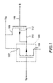
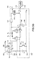
- the sensor device shown in Fig. 1 comprises a Radiation sensor element, which in its entirety with the Reference numeral 100 is provided.
- This radiation sensor element is an exemplary embodiment 100, for example, a MOS transistor, the so-called has floating tub.
- the present invention is not is limited to such radiation sensor elements, but that a variety of radiation sensor elements in question come, such as a J-FET or an SOI transistor.
- the drain-source current of transistor 100 is essentially proportional to the incident radiation power.
- a source terminal 102 of transistor 100 is supplied with a supply potential V DD , while the operating point of the transistor can be set via an operating point setting voltage V B.
- the signal generated by transistor 100 can be tapped at a drain terminal 104 of transistor 100.
- the output signal tapped at the drain terminal 104 becomes fed to a detection circuit (not shown in FIG. 1), that generated by the radiation sensor element Electricity recorded and processed.
- the radiation sensor device shown in Fig. 1 comprises in addition to transistor 100, a reset circuit that in the embodiment shown in Fig. 1 FET switch is on.
- the FET switch includes a gate terminal 106, one Source terminal 108, a drain terminal 110 and one with the substrate terminal 112 connected to the drain terminal 110.
- the source terminal 108 is supplied with the supply potential V DD .
- a reset signal R can be applied to the gate connection 106, generated by the detection circuit (not shown) becomes.
- the radiation sensor element 100 is a MOS transistor with floating tub, so the reset circuit in this Trough be arranged, which gives the advantage that the reset circuit is not part of the active area of the Radiation sensor device is.
- the present invention is not limited to FET switches, it is essentially any type a reset circuit can be used, which makes it possible the recombination rate by applying a reset signal compared to the recombination rate without a reset signal to increase.
- FIG a reset circuit Although only one radiation sensor element is shown in FIG a reset circuit, it is obvious that the invention is not limited to this single element is limited, but also the interconnection of a A plurality of such radiation sensor elements with a reset circuit in a matrix.
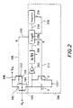
- FIG. 2 shows an exemplary embodiment of a detection circuit which is shown in FIG is designated in its entirety with reference number 200.
- This detection circuit 200 comprises a capacitor C, that between the output 104 of the radiation sensor element 100 and ground is switched.
- a switch S is in parallel to the capacitor C and bridges this in its closed Status.
- the switch S is one FET switch known per se. The representation of this FET switch is only an example, other switch devices can easily replace the FET switch be used.
- the output 104 of the radiation sensor element 100 is included connected to an input of a buffer 202, the output of which connected to the input of an analog / digital converter 204 is.
- a logic circuit 206 includes an input 208 which connected to the output of the analog / digital converter 204 and three outputs 210, 212 and 214. Depending on am The logic circuit generates signals applied to input 208 206 at the first output 210 and at the second output 212 Reset signal R.
- the output 210 of logic circuit 206 is connected to the gate terminal 106 of the reset circuit, and the output 212 of logic circuit 206 is connected to that Gate terminal of the switch S connected.
- the logic circuit 206 generates an output signal at its third output 214, which is entered into a flag memory 216.
- Logic circuit 206 operates to only reset the matrix element (pixel) if the result is valid or the pixel was not reset in the previous cycle.
- the following table shows the algorithm used: Result of the A / D conversion Old value of the readout flag New value of the readout flag Result Minimum or maximum any 0 valid other digital word 0 1 invalid other digital word 1 0 valid
- This algorithm ensures that regardless of Arrival of an event - the arrival of radiation on a sensor element - at least one system period passes. That is why the result is falsified not to be expected.
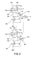
- Fig. 3 shows a so-called intelligent addressing, which saves addressing on the chip surface can be.
- the advantage is that on the Sensor surface essentially only remains active area.
- Fig. 3 is part of a detection circuit shown.
- the detection circuit in Fig. 3 comprises a first transistor 300 between the output of the radiation sensor element 104 and ground is switched, and a second Transistor 302 connected to the output of the radiation sensor element 104 is connected.
- Transistors 300, 302 ensure that during the Reset phase, the signals at output 104 of the radiation sensor element 100 lie on ground.
- the signal at output 304 is exactly appear with the highest level.
- the embodiment shown in Fig. 3 has one A plurality of such detection circuits on whose outputs 304 each connected to the input of a buffer 306 are, the output with another, not shown Part of a detection circuit is connected.
- a reset signal can be applied to the first transistor.
- This intelligent addressing enables that the pixel at which the signal is applied always has the output signal certainly. As soon as a value has been read out or has elapsed a predetermined time, the reset signal spent.
- the first transistor 300 is designed as an NMOS transistor, its source with the output 104 of the radiation sensor element 100 is connected, the drain of which is connected to ground is, and at the gate of the reset signal can be applied.
- the second transistor 302 is an NMOS transistor, which in the so-called diode circuit is connected.
- FIG. 4 A fourth exemplary embodiment is described below with reference to FIG. 4 of the present invention.
- elements that have already been described with reference to FIG. 1 have been provided with the same reference numerals and a renewed description is omitted.
- the detection circuit 400 in the exemplary embodiment in FIG. 4 comprises a first storage capacitor C 1 , the first connection 402 of which is connected to the output 104 of the radiation sensor element 100, and the second connection 404 of which is connected to a power supply V SS .
- a first reset switch R 1 is connected in parallel with the first storage capacitor.
- the detection circuit 400 further comprises a second storage capacitor C 2 , the first connection 406 of which is connected to an output 408 of the detection circuit 400, and the second connection 410 of which is connected to the power supply V ss .
- a second reset switch R 2 is connected in parallel with the second storage capacitor.
- the reset switches R 1 and R 2 are FET switches in this exemplary embodiment.
- An inverting input of a comparator K is connected to the first connection 402 of the first storage capacitor C 1 , and a non-inverting connection of the comparator K is connected to the first connection 406 of the second storage capacitor C 2 .
- a switch S 1 is connected between the output 104 of the radiation sensor element 100 and the output 408 of the detection circuit 400.
- the switch is controlled by a signal at the output of the comparator K and, in its closed state, connects the output 104 and the output 408.
- the output of the comparator is connected to an input 412 of a register REG.
- An output 414 of the register REG is connected to a read terminal 416 of the detection circuit 400.
- a reset input 418 of the register REG is connected to a reset terminal R 3 .
- an output signal of the radiation sensor element 100 is stored on the storage capacitor C 2 . Thereafter, the radiation sensor element 100 is reset.
- the output signal of the radiation sensor element 100 is stored on the storage capacitor C 1 .
- the storage capacitor C 1 is discharged by the first reset switch R. 1
- the voltages across the storage capacitors C 1 and C 2 are compared by the comparator. If the voltage at the storage capacitor C 1 is greater than that at the storage capacitor C 2 , a signal is generated at the output of the comparator.
- This signal causes switch S 1 to be closed , which is open at the beginning of the measuring time. At the same time, a read bit is written into the register REG.
- the readout from the detection circuit 400 is carried out only in the case in which the readout bit is set.
- the readout bit is reset by a reset signal which is present at the reset connection R 3 .
- the reading is controlled by a processing circuit (not shown) arranged at the output 408 of the detection circuit 400.
- both storage capacitors are reset by means of the reset switches R 1 and R 2 before a new measurement.
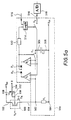
- the intrinsic capacitance C n of the radiation sensor element 100 serves as a memory for the radiation incident on the radiation sensor element 100, as is shown in FIGS. 5a and 5b.
- this intrinsic capacitance C n is the N-well capacitance of the P-MOS phototransistor.
- the detection circuit 500 in the exemplary embodiment shown in FIG. 5a comprises a resistor R 1 , the first connection 502 of which is connected to the output 104 of the radiation sensor element and the second connection 504 of which is connected to a power supply V SS .
- the resistor R 1 has its first connection 502 connected to an inverting connection of a first comparator K 1 and to a non-inverting connection of a second comparator K 2 .
- the first connection 502 of the resistor R 1 is connected to a first connection 506 of a storage capacitor C 2 via a first switch S 1 .
- the storage capacitor C 2 has a second connection 508, which is connected to the power supply V SS .
- the storage capacitor C 2 has its first connection 506 connected to a non-inverting connection of the comparator K 1 and to an inverting connection of the comparator K 2 .
- the storage capacitor C 2 has its first connection 506 connected to an output 510 of the detection circuit 500 via a second switch S 2 .
- the outputs of the comparators K 1 , K 2 are connected to one another via two diodes D 1 and D 2 .
- the output signal of the comparators K 1 , K 2 can be tapped between the diodes D 1 and D 2 .
- the first switch S 1 can be controlled by means of this output signal.
- the output signal of the comparators K 1 , K 2 can be applied to the second switch S 2 for controlling it via a delay circuit 512 and a logic circuit 514.
- the logic circuit 514 receives an external control signal via a connection 516.
- the output of the detection circuit is via an A / D converter 518 connected to a data bus (not shown).
- the current generated by the radiation sensor element 100 is registered at the resistor R 1 as a voltage drop.
- the double comparator K 1 , K 2 compares the voltages across the resistor R 1 and across the storage capacitor C 2 . If both voltages are equal, the first switch S 1 is not closed and no output signal is sent to the second switch S 2 for pulse height processing.
- the first switch S 1 is closed and the storage capacitor C 2 is charged to the potential at the resistor R 1 .
- the output signal is sent via the second switch S 2 to the A / D converter 518 and to the data bus with a slight time delay until the charging process is completed.
- the second switch S 2 and the first switch S 1 are opened and the storage capacitor C 2 stores the charge.
- the radiation sensor element 100 and its intrinsic capacitance C n are then reset.
- This process runs during a defined clock cycle from.
- a first storage capacitor C 1 is used in the detection circuit 500 'according to this exemplary embodiment, to which a reset switch RS is connected in parallel, to which a reset signal R rs can be applied.
- a buffer P which has a gain of one, is provided between the non-inverting input of the comparator K 2 and the first switch S 1 .
- the first storage capacitor C 1 is charged by the current flow resulting from the radiation incident.
- the charges on the first storage capacitor C 1 and the storage capacitor C 2 are compared at defined time intervals.
- the switch S 1 is closed and the charge is transferred from the first storage capacitor C 1 to the storage capacitor C 2 via the buffer P and its low-resistance output.
- the storage capacitor C 2 by means of the second switch S 2 to the output of the detection circuit is connected 500 '.
- both the intrinsic capacitance C n of the radiation sensor element 100 and the first storage capacitor C 1 are reset by means of the reset signals R and R rs .
- the incident Photon current corresponds to the number of photons per Time.
- the processing dynamics can be determined, by specifying how many cycles the quantized Pixel signal in the processing unit to one Data value is composed. Through this procedure very elegantly simplifies the A / D conversion and at the same time data reduction is achieved.
- the interface system between the pixel matrix and the processing unit is thereby related to several orders of magnitude relieved of the data flow.
- New video systems with refresh rates for extreme fast events and for process control are possible.
- aperture systems can be dispensed with, because the dynamic range is high enough.
Landscapes
- Physics & Mathematics (AREA)
- General Physics & Mathematics (AREA)
- Engineering & Computer Science (AREA)
- Power Engineering (AREA)
- Spectroscopy & Molecular Physics (AREA)
- Microelectronics & Electronic Packaging (AREA)
- Condensed Matter Physics & Semiconductors (AREA)
- Computer Hardware Design (AREA)
- Electromagnetism (AREA)
- Multimedia (AREA)
- Signal Processing (AREA)
- Measurement Of Radiation (AREA)
- Light Receiving Elements (AREA)
- Transforming Light Signals Into Electric Signals (AREA)
- Photometry And Measurement Of Optical Pulse Characteristics (AREA)
- Analysing Materials By The Use Of Radiation (AREA)
Applications Claiming Priority (3)
| Application Number | Priority Date | Filing Date | Title |
|---|---|---|---|
| DE19510070A DE19510070C1 (de) | 1995-03-20 | 1995-03-20 | Strahlungssensoreinrichtung zum Erfassen der Häufigkeit einer auf diese auftreffenden Strahlung |
| DE19510070 | 1995-03-20 | ||
| PCT/EP1996/001074 WO1996029820A1 (de) | 1995-03-20 | 1996-03-13 | Strahlungssensoreinrichtung zum erfassen der häufigkeit einer auf dieser auftreffenden strahlung |
Publications (2)
| Publication Number | Publication Date |
|---|---|
| EP0806109A1 EP0806109A1 (de) | 1997-11-12 |
| EP0806109B1 true EP0806109B1 (de) | 1998-06-10 |
Family
ID=7757174
Family Applications (1)
| Application Number | Title | Priority Date | Filing Date |
|---|---|---|---|
| EP96906764A Expired - Lifetime EP0806109B1 (de) | 1995-03-20 | 1996-03-13 | Strahlungssensoreinrichtung zum erfassen der häufigkeit einer auf dieser auftreffenden strahlung |
Country Status (7)
| Country | Link |
|---|---|
| US (1) | US5969336A (ja) |
| EP (1) | EP0806109B1 (ja) |
| JP (1) | JP2986922B2 (ja) |
| KR (1) | KR100265139B1 (ja) |
| AT (1) | ATE167346T1 (ja) |
| DE (2) | DE19510070C1 (ja) |
| WO (1) | WO1996029820A1 (ja) |
Families Citing this family (4)
| Publication number | Priority date | Publication date | Assignee | Title |
|---|---|---|---|---|
| FI954041A0 (fi) * | 1995-08-28 | 1995-08-28 | Hidex Oy | Foerfarande foer detektering av radioaktivitet i ett stoedmaterial genom direkt detektering av jonisation |
| DE19729606C2 (de) * | 1997-07-10 | 2000-06-29 | Thomas Streil | Strahlungssensorvorrichtung |
| DE19953255A1 (de) | 1999-11-04 | 2001-05-10 | Khs Masch & Anlagenbau Ag | Etikettiermaschine für Gegenstände |
| WO2023190086A1 (ja) * | 2022-03-29 | 2023-10-05 | ヌヴォトンテクノロジージャパン株式会社 | 放射線量検知装置および放射線量検知方法 |
Family Cites Families (4)
| Publication number | Priority date | Publication date | Assignee | Title |
|---|---|---|---|---|
| JPS639288A (ja) * | 1986-06-30 | 1988-01-14 | Toshiba Corp | 固体撮像素子の駆動方法 |
| DE4118154A1 (de) * | 1991-06-03 | 1992-12-10 | Philips Patentverwaltung | Anordnung mit einer sensormatrix und einer ruecksetzanordnung |
| JPH0522516A (ja) * | 1991-07-17 | 1993-01-29 | Fuji Xerox Co Ltd | イメージセンサ |
| DE4224358C1 (de) * | 1992-07-23 | 1993-10-28 | Fraunhofer Ges Forschung | Strahlungssensoreinrichtung |
-
1995
- 1995-03-20 DE DE19510070A patent/DE19510070C1/de not_active Expired - Fee Related
-
1996
- 1996-03-13 AT AT96906764T patent/ATE167346T1/de not_active IP Right Cessation
- 1996-03-13 US US08/913,643 patent/US5969336A/en not_active Expired - Fee Related
- 1996-03-13 EP EP96906764A patent/EP0806109B1/de not_active Expired - Lifetime
- 1996-03-13 WO PCT/EP1996/001074 patent/WO1996029820A1/de active IP Right Grant
- 1996-03-13 KR KR1019970706540A patent/KR100265139B1/ko not_active IP Right Cessation
- 1996-03-13 DE DE59600278T patent/DE59600278D1/de not_active Expired - Fee Related
- 1996-03-13 JP JP8528050A patent/JP2986922B2/ja not_active Expired - Fee Related
Also Published As
| Publication number | Publication date |
|---|---|
| KR19980703137A (ko) | 1998-10-15 |
| ATE167346T1 (de) | 1998-06-15 |
| JPH10512416A (ja) | 1998-11-24 |
| JP2986922B2 (ja) | 1999-12-06 |
| EP0806109A1 (de) | 1997-11-12 |
| DE59600278D1 (de) | 1998-07-16 |
| US5969336A (en) | 1999-10-19 |
| DE19510070C1 (de) | 1996-08-08 |
| KR100265139B1 (ko) | 2000-09-01 |
| WO1996029820A1 (de) | 1996-09-26 |
Similar Documents
| Publication | Publication Date | Title |
|---|---|---|
| DE102010041805B4 (de) | Vorrichtung mit mehreren zeilen- oder matrixförmig angeordneten photoempfindlichen Mikrozellen | |
| DE60125097T2 (de) | Kapatizitives Sensorgerät zur Erkennung kleiner Muster | |
| DE2936703C2 (ja) | ||
| DE2939490C2 (ja) | ||
| DE19610555C2 (de) | Leckspannungs-Detektorschaltung für einen MOS Kondensator | |
| DE2609731A1 (de) | Festkoerper-bilderfassungsvorrichtung | |
| DE2707456C3 (ja) | ||
| DE3630679C2 (ja) | ||
| DE4205578A1 (de) | Halbleiterspeichereinrichtung mit adressuebergangsdetektor | |
| EP0806109B1 (de) | Strahlungssensoreinrichtung zum erfassen der häufigkeit einer auf dieser auftreffenden strahlung | |
| DE3105910C2 (ja) | ||
| EP1078371B1 (de) | Schaltungsanordnung mit einem sensorelement und einem nichtflüchtigen speichermittel | |
| DE2234310A1 (de) | Logischer schaltkreis mit mindestens einer taktleitung | |
| WO1995008190A1 (de) | Halbleiter(detektor)struktur | |
| DE1960598A1 (de) | MOS-Schnellesespeicher | |
| DE3923630C2 (ja) | ||
| EP0510408B1 (de) | Photodetektoranordnung | |
| DE60214078T2 (de) | Erfassungsvorrichtung zur Erkennung von Oberflächenmustern | |
| DE2936492C2 (ja) | ||
| EP1379940B1 (de) | Zufallszahlengenerator und verfahren zum erzeugen einer zufallszahl | |
| DE3615925C2 (ja) | ||
| EP1128248A1 (de) | Halbleiterchip mit einem lichtempfindlichen Element | |
| DE3245008A1 (de) | Amplitudenregelsystem | |
| DE19729606C2 (de) | Strahlungssensorvorrichtung | |
| DE4443821A1 (de) | Bildaufnahmevorrichtung |
Legal Events
| Date | Code | Title | Description |
|---|---|---|---|
| PUAI | Public reference made under article 153(3) epc to a published international application that has entered the european phase |
Free format text: ORIGINAL CODE: 0009012 |
|
| 17P | Request for examination filed |
Effective date: 19970910 |
|
| AK | Designated contracting states |
Kind code of ref document: A1 Designated state(s): AT BE CH DE FR GB LI |
|
| GRAG | Despatch of communication of intention to grant |
Free format text: ORIGINAL CODE: EPIDOS AGRA |
|
| GRAG | Despatch of communication of intention to grant |
Free format text: ORIGINAL CODE: EPIDOS AGRA |
|
| GRAH | Despatch of communication of intention to grant a patent |
Free format text: ORIGINAL CODE: EPIDOS IGRA |
|
| 17Q | First examination report despatched |
Effective date: 19971127 |
|
| GRAH | Despatch of communication of intention to grant a patent |
Free format text: ORIGINAL CODE: EPIDOS IGRA |
|
| GRAA | (expected) grant |
Free format text: ORIGINAL CODE: 0009210 |
|
| AK | Designated contracting states |
Kind code of ref document: B1 Designated state(s): AT BE CH DE FR GB LI |
|
| PG25 | Lapsed in a contracting state [announced via postgrant information from national office to epo] |
Ref country code: GB Free format text: LAPSE BECAUSE OF FAILURE TO SUBMIT A TRANSLATION OF THE DESCRIPTION OR TO PAY THE FEE WITHIN THE PRESCRIBED TIME-LIMIT Effective date: 19980610 Ref country code: FR Free format text: LAPSE BECAUSE OF FAILURE TO SUBMIT A TRANSLATION OF THE DESCRIPTION OR TO PAY THE FEE WITHIN THE PRESCRIBED TIME-LIMIT Effective date: 19980610 |
|
| REF | Corresponds to: |
Ref document number: 167346 Country of ref document: AT Date of ref document: 19980615 Kind code of ref document: T |
|
| REG | Reference to a national code |
Ref country code: CH Ref legal event code: EP |
|
| REF | Corresponds to: |
Ref document number: 59600278 Country of ref document: DE Date of ref document: 19980716 |
|
| EN | Fr: translation not filed | ||
| GBV | Gb: ep patent (uk) treated as always having been void in accordance with gb section 77(7)/1977 [no translation filed] |
Effective date: 19980610 |
|
| PG25 | Lapsed in a contracting state [announced via postgrant information from national office to epo] |
Ref country code: AT Free format text: LAPSE BECAUSE OF NON-PAYMENT OF DUE FEES Effective date: 19990313 |
|
| PG25 | Lapsed in a contracting state [announced via postgrant information from national office to epo] |
Ref country code: BE Free format text: LAPSE BECAUSE OF NON-PAYMENT OF DUE FEES Effective date: 19990331 |
|
| PLBE | No opposition filed within time limit |
Free format text: ORIGINAL CODE: 0009261 |
|
| STAA | Information on the status of an ep patent application or granted ep patent |
Free format text: STATUS: NO OPPOSITION FILED WITHIN TIME LIMIT |
|
| 26N | No opposition filed | ||
| BERE | Be: lapsed |
Owner name: SARAD G.- FUR KOMPLEXE LEISTUNGEN ZUR SANIERUNG R Effective date: 19990331 |
|
| PGFP | Annual fee paid to national office [announced via postgrant information from national office to epo] |
Ref country code: DE Payment date: 20000821 Year of fee payment: 5 |
|
| REG | Reference to a national code |
Ref country code: CH Ref legal event code: PL |
|
| PGFP | Annual fee paid to national office [announced via postgrant information from national office to epo] |
Ref country code: CH Payment date: 20010213 Year of fee payment: 5 |
|
| REG | Reference to a national code |
Ref country code: CH Ref legal event code: AEN Free format text: DAS PATENT IST AUFGRUND DES WEITERBEHANDLUNGSANTRAGS VOM 21.12.2000 REAKTIVIERT WORDEN. |
|
| PG25 | Lapsed in a contracting state [announced via postgrant information from national office to epo] |
Ref country code: LI Free format text: LAPSE BECAUSE OF NON-PAYMENT OF DUE FEES Effective date: 20010331 Ref country code: DE Free format text: LAPSE BECAUSE OF NON-PAYMENT OF DUE FEES Effective date: 20010331 Ref country code: CH Free format text: LAPSE BECAUSE OF NON-PAYMENT OF DUE FEES Effective date: 20010331 |
|
| REG | Reference to a national code |
Ref country code: CH Ref legal event code: PL |