WO2023190086A1 - 放射線量検知装置および放射線量検知方法 - Google Patents
放射線量検知装置および放射線量検知方法 Download PDFInfo
- Publication number
- WO2023190086A1 WO2023190086A1 PCT/JP2023/011651 JP2023011651W WO2023190086A1 WO 2023190086 A1 WO2023190086 A1 WO 2023190086A1 JP 2023011651 W JP2023011651 W JP 2023011651W WO 2023190086 A1 WO2023190086 A1 WO 2023190086A1
- Authority
- WO
- WIPO (PCT)
- Prior art keywords
- radiation dose
- circuit
- current
- radiation
- power supply
- Prior art date
Links
- 230000005855 radiation Effects 0.000 title claims abstract description 185
- 238000000034 method Methods 0.000 title description 11
- 229910000314 transition metal oxide Inorganic materials 0.000 claims abstract description 11
- 238000001514 detection method Methods 0.000 claims description 111
- BPUBBGLMJRNUCC-UHFFFAOYSA-N oxygen(2-);tantalum(5+) Chemical compound [O-2].[O-2].[O-2].[O-2].[O-2].[Ta+5].[Ta+5] BPUBBGLMJRNUCC-UHFFFAOYSA-N 0.000 claims description 10
- 229910001936 tantalum oxide Inorganic materials 0.000 claims description 10
- 229910000449 hafnium oxide Inorganic materials 0.000 claims description 2
- WIHZLLGSGQNAGK-UHFFFAOYSA-N hafnium(4+);oxygen(2-) Chemical compound [O-2].[O-2].[Hf+4] WIHZLLGSGQNAGK-UHFFFAOYSA-N 0.000 claims description 2
- TWNQGVIAIRXVLR-UHFFFAOYSA-N oxo(oxoalumanyloxy)alumane Chemical compound O=[Al]O[Al]=O TWNQGVIAIRXVLR-UHFFFAOYSA-N 0.000 claims description 2
- RVTZCBVAJQQJTK-UHFFFAOYSA-N oxygen(2-);zirconium(4+) Chemical compound [O-2].[O-2].[Zr+4] RVTZCBVAJQQJTK-UHFFFAOYSA-N 0.000 claims description 2
- 229910001928 zirconium oxide Inorganic materials 0.000 claims description 2
- 230000008859 change Effects 0.000 abstract description 39
- 230000006870 function Effects 0.000 abstract description 24
- 230000001419 dependent effect Effects 0.000 abstract description 3
- 239000010410 layer Substances 0.000 description 48
- 206010073306 Exposure to radiation Diseases 0.000 description 45
- 238000010586 diagram Methods 0.000 description 14
- 239000004065 semiconductor Substances 0.000 description 13
- 230000000875 corresponding effect Effects 0.000 description 11
- 230000010355 oscillation Effects 0.000 description 6
- 229910052751 metal Inorganic materials 0.000 description 5
- 239000002184 metal Substances 0.000 description 5
- QVGXLLKOCUKJST-UHFFFAOYSA-N atomic oxygen Chemical compound [O] QVGXLLKOCUKJST-UHFFFAOYSA-N 0.000 description 4
- 230000000694 effects Effects 0.000 description 4
- 238000004519 manufacturing process Methods 0.000 description 4
- 239000000463 material Substances 0.000 description 4
- 238000005259 measurement Methods 0.000 description 4
- 229910052760 oxygen Inorganic materials 0.000 description 4
- 239000001301 oxygen Substances 0.000 description 4
- 229910052723 transition metal Inorganic materials 0.000 description 4
- 150000003624 transition metals Chemical class 0.000 description 4
- PXHVJJICTQNCMI-UHFFFAOYSA-N Nickel Chemical compound [Ni] PXHVJJICTQNCMI-UHFFFAOYSA-N 0.000 description 3
- 238000004891 communication Methods 0.000 description 3
- 238000007689 inspection Methods 0.000 description 3
- 238000004377 microelectronic Methods 0.000 description 3
- 238000012544 monitoring process Methods 0.000 description 3
- BASFCYQUMIYNBI-UHFFFAOYSA-N platinum Substances [Pt] BASFCYQUMIYNBI-UHFFFAOYSA-N 0.000 description 3
- 239000000758 substrate Substances 0.000 description 3
- 230000007704 transition Effects 0.000 description 3
- NRTOMJZYCJJWKI-UHFFFAOYSA-N Titanium nitride Chemical compound [Ti]#N NRTOMJZYCJJWKI-UHFFFAOYSA-N 0.000 description 2
- 229910052782 aluminium Inorganic materials 0.000 description 2
- XAGFODPZIPBFFR-UHFFFAOYSA-N aluminium Chemical compound [Al] XAGFODPZIPBFFR-UHFFFAOYSA-N 0.000 description 2
- 230000008901 benefit Effects 0.000 description 2
- 239000010949 copper Substances 0.000 description 2
- 238000012937 correction Methods 0.000 description 2
- 230000001186 cumulative effect Effects 0.000 description 2
- 230000007423 decrease Effects 0.000 description 2
- 230000002542 deteriorative effect Effects 0.000 description 2
- 238000005516 engineering process Methods 0.000 description 2
- 230000002427 irreversible effect Effects 0.000 description 2
- 239000010955 niobium Substances 0.000 description 2
- 239000005022 packaging material Substances 0.000 description 2
- 230000008569 process Effects 0.000 description 2
- 238000012545 processing Methods 0.000 description 2
- 230000001954 sterilising effect Effects 0.000 description 2
- 238000004659 sterilization and disinfection Methods 0.000 description 2
- 229910052715 tantalum Inorganic materials 0.000 description 2
- GUVRBAGPIYLISA-UHFFFAOYSA-N tantalum atom Chemical compound [Ta] GUVRBAGPIYLISA-UHFFFAOYSA-N 0.000 description 2
- 239000010936 titanium Substances 0.000 description 2
- 238000009966 trimming Methods 0.000 description 2
- WFKWXMTUELFFGS-UHFFFAOYSA-N tungsten Chemical compound [W] WFKWXMTUELFFGS-UHFFFAOYSA-N 0.000 description 2
- 229910052721 tungsten Inorganic materials 0.000 description 2
- 239000010937 tungsten Substances 0.000 description 2
- 238000012935 Averaging Methods 0.000 description 1
- RYGMFSIKBFXOCR-UHFFFAOYSA-N Copper Chemical compound [Cu] RYGMFSIKBFXOCR-UHFFFAOYSA-N 0.000 description 1
- XEEYBQQBJWHFJM-UHFFFAOYSA-N Iron Chemical compound [Fe] XEEYBQQBJWHFJM-UHFFFAOYSA-N 0.000 description 1
- RTAQQCXQSZGOHL-UHFFFAOYSA-N Titanium Chemical compound [Ti] RTAQQCXQSZGOHL-UHFFFAOYSA-N 0.000 description 1
- UQZIWOQVLUASCR-UHFFFAOYSA-N alumane;titanium Chemical compound [AlH3].[Ti] UQZIWOQVLUASCR-UHFFFAOYSA-N 0.000 description 1
- 239000002131 composite material Substances 0.000 description 1
- 239000000470 constituent Substances 0.000 description 1
- 229910052802 copper Inorganic materials 0.000 description 1
- 230000002596 correlated effect Effects 0.000 description 1
- 238000013500 data storage Methods 0.000 description 1
- 230000002950 deficient Effects 0.000 description 1
- 230000000593 degrading effect Effects 0.000 description 1
- 238000013461 design Methods 0.000 description 1
- 231100000673 dose–response relationship Toxicity 0.000 description 1
- 230000002349 favourable effect Effects 0.000 description 1
- 235000013305 food Nutrition 0.000 description 1
- 229910052735 hafnium Inorganic materials 0.000 description 1
- VBJZVLUMGGDVMO-UHFFFAOYSA-N hafnium atom Chemical compound [Hf] VBJZVLUMGGDVMO-UHFFFAOYSA-N 0.000 description 1
- 230000009931 harmful effect Effects 0.000 description 1
- 239000011229 interlayer Substances 0.000 description 1
- 229910052741 iridium Inorganic materials 0.000 description 1
- GKOZUEZYRPOHIO-UHFFFAOYSA-N iridium atom Chemical compound [Ir] GKOZUEZYRPOHIO-UHFFFAOYSA-N 0.000 description 1
- 238000012886 linear function Methods 0.000 description 1
- 230000007257 malfunction Effects 0.000 description 1
- 238000007726 management method Methods 0.000 description 1
- 238000012986 modification Methods 0.000 description 1
- 230000004048 modification Effects 0.000 description 1
- 229910052759 nickel Inorganic materials 0.000 description 1
- 229910052758 niobium Inorganic materials 0.000 description 1
- GUCVJGMIXFAOAE-UHFFFAOYSA-N niobium atom Chemical compound [Nb] GUCVJGMIXFAOAE-UHFFFAOYSA-N 0.000 description 1
- 230000003647 oxidation Effects 0.000 description 1
- 238000007254 oxidation reaction Methods 0.000 description 1
- 230000002093 peripheral effect Effects 0.000 description 1
- 229910052697 platinum Inorganic materials 0.000 description 1
- 238000006479 redox reaction Methods 0.000 description 1
- 238000011160 research Methods 0.000 description 1
- 230000004044 response Effects 0.000 description 1
- VSZWPYCFIRKVQL-UHFFFAOYSA-N selanylidenegallium;selenium Chemical compound [Se].[Se]=[Ga].[Se]=[Ga] VSZWPYCFIRKVQL-UHFFFAOYSA-N 0.000 description 1
- 235000013599 spices Nutrition 0.000 description 1
- MZLGASXMSKOWSE-UHFFFAOYSA-N tantalum nitride Chemical compound [Ta]#N MZLGASXMSKOWSE-UHFFFAOYSA-N 0.000 description 1
- 229910052719 titanium Inorganic materials 0.000 description 1
Images


Classifications
-
- G—PHYSICS
- G01—MEASURING; TESTING
- G01T—MEASUREMENT OF NUCLEAR OR X-RADIATION
- G01T1/00—Measuring X-radiation, gamma radiation, corpuscular radiation, or cosmic radiation
- G01T1/16—Measuring radiation intensity
-
- G—PHYSICS
- G01—MEASURING; TESTING
- G01T—MEASUREMENT OF NUCLEAR OR X-RADIATION
- G01T1/00—Measuring X-radiation, gamma radiation, corpuscular radiation, or cosmic radiation
- G01T1/16—Measuring radiation intensity
- G01T1/17—Circuit arrangements not adapted to a particular type of detector
-
- G—PHYSICS
- G11—INFORMATION STORAGE
- G11C—STATIC STORES
- G11C13/00—Digital stores characterised by the use of storage elements not covered by groups G11C11/00, G11C23/00, or G11C25/00
-
- H—ELECTRICITY
- H10—SEMICONDUCTOR DEVICES; ELECTRIC SOLID-STATE DEVICES NOT OTHERWISE PROVIDED FOR
- H10B—ELECTRONIC MEMORY DEVICES
- H10B63/00—Resistance change memory devices, e.g. resistive RAM [ReRAM] devices
-
- H—ELECTRICITY
- H10—SEMICONDUCTOR DEVICES; ELECTRIC SOLID-STATE DEVICES NOT OTHERWISE PROVIDED FOR
- H10B—ELECTRONIC MEMORY DEVICES
- H10B99/00—Subject matter not provided for in other groups of this subclass
-
- H—ELECTRICITY
- H10—SEMICONDUCTOR DEVICES; ELECTRIC SOLID-STATE DEVICES NOT OTHERWISE PROVIDED FOR
- H10N—ELECTRIC SOLID-STATE DEVICES NOT OTHERWISE PROVIDED FOR
- H10N70/00—Solid-state devices without a potential-jump barrier or surface barrier, and specially adapted for rectifying, amplifying, oscillating or switching
-
- H—ELECTRICITY
- H10—SEMICONDUCTOR DEVICES; ELECTRIC SOLID-STATE DEVICES NOT OTHERWISE PROVIDED FOR
- H10N—ELECTRIC SOLID-STATE DEVICES NOT OTHERWISE PROVIDED FOR
- H10N99/00—Subject matter not provided for in other groups of this subclass
Definitions
- the present disclosure relates to a radiation dose detection device and a radiation dose detection method, and more particularly to a radiation dose detection device that has a function that enables response to changes in characteristics due to exposure to radiation.
- RF tags For example, medical equipment, pharmaceutical containers, and food products such as spices are sterilized by radiation.
- the RF tags In order to attach RF tags to such products and packaging materials and ensure product inventory management and traceability, the RF tags must function normally even after radiation exposure.
- the RF tag has a sensing function such as a radiation sensor or a temperature sensor, as exemplified in Patent Document 1, the sensing accuracy is required to maintain a predetermined performance.
- semiconductor integrated circuits are generally provided with a regulator circuit to generate an operating voltage within the integrated circuit from an externally input power supply voltage. Then, in order for the regulator circuit to generate a predetermined voltage, a bandgap reference circuit that generates a reference voltage that is a reference for the regulator circuit is installed. Since the regulator circuit and the bandgap reference circuit are well-known technologies, detailed explanations thereof will be omitted here.
- variations in the reference voltage generated by the bandgap reference circuit are trimmed and adjusted during pre-shipment inspection of the RF tag so that a desired voltage is output.
- the power supply voltage output by the regulator circuit is also adjusted to a voltage within a predetermined range.
- an RF tag similarly equipped with a sensor element undergoes calibration of its sensing operation during post-manufacturing inspection. For example, in the case of a temperature sensor, all RF tags calibrate the relationship between the physical quantity obtained from the sensor element and temperature (in other words, temperature characteristics) under the power supply voltage adjusted to a predetermined range, and then Make sure the exact temperature corresponds.
- the threshold voltage VT of the transistor changes due to exposure to radiation in the field after shipment, the reference voltage changes compared to before exposure, and the generated power supply voltage changes accordingly.
- the relationship between the physical quantity obtained from the sensor element and temperature will change, making it impossible to obtain accurate temperature.
- This also applies to radiation detection circuits using radiation sensor elements. If the tag is exposed to a higher radiation dose and the shift in the threshold voltage VT becomes large and the power supply voltage fluctuates beyond the tag's normal operating limit, the RF tag itself will malfunction.
- Patent Document 2 exemplifies a method of monitoring the effect on a semiconductor integrated circuit and measuring the amount of exposure when the circuit is exposed to radiation.
- Patent Document 2 proposes monitoring the amount of radiation exposure by utilizing the fact that the frequency of pulses generated by a ring oscillator mounted on a semiconductor integrated circuit changes depending on the amount of exposure to radiation.
- Patent Document 3 discloses a method for monitoring the ambient temperature of a semiconductor integrated circuit by making use of the property that the resistance value of a variable resistance element changes depending on the temperature, and changing the oscillation frequency of an oscillator based on the resistance depending on the temperature. is proposed.
- Patent No. 6487070 JP 61-161480 Publication Japanese Patent Application Publication No. 2016-31274
- Patent Documents 1 to 3 are not able to cope with the problem that the sensing accuracy is degraded due to the influence of power supply voltage fluctuations due to exposure to radiation as described above.
- RF tags to sense and collect information on temperature, radiation, and other surrounding environments as in the previous example mentioned above
- the transistors that make up the sensor suffer irreversible damage, and the power supply voltage fluctuates from the beginning, making it impossible to perform normal sensing or deteriorating accuracy.
- the present disclosure provides a radiation dose detection device having a function of detecting not only radiation dose but also temperature and making it possible to respond to changes in characteristics due to exposure to radiation, and a radiation dose detection device using such a radiation dose detection device.
- the purpose is to provide a radiation dose detection method.
- a radiation dose detection device includes a power supply circuit that outputs a power supply voltage, and a first circuit that uses the power supply voltage and is dependent on the ambient temperature of the radiation dose detection device. a first current source that outputs a current; a second current source that uses the power supply voltage to output a second current that depends on the radiation dose irradiated by the radiation dose detection device; and a magnitude of the first current.
- a detection circuit that outputs a first signal indicative of a temperature corresponding to the magnitude of the second current, and a detection circuit that outputs a second signal indicative of a radiation dose corresponding to the magnitude of the second current, the first current source , a second electrode layer, and one or more variable resistance elements having a variable resistance layer containing a transition metal oxide interposed between the first electrode layer and the second electrode layer; a first node that connects the first electrode layers of the variable resistance elements; and a second node that connects the second electrode layers of the one or more variable resistance elements;
- the power supply voltage is applied to one node, the second node outputs the first current, the second current source includes a transistor, and one terminal of the transistor is applied with the power supply voltage. is applied, and the other terminal of the transistor outputs the second current.
- a radiation dose detection method is a radiation dose detection method using the radiation dose detection device, wherein the selection circuit selects the first a first acquisition step of acquiring a first correlation between the ambient temperature and the count value output by the counter circuit with the current selected; and after irradiation with radiation, the selection circuit selects the first current.
- the method includes an adjusting step of adjusting a voltage, and a radiation dose detecting step of detecting a radiation dose after the adjusting step with the selection circuit selecting the second current.
- the present disclosure provides a radiation dose detection device that has a function of detecting not only radiation dose but also temperature and making it possible to respond to changes in characteristics due to exposure to radiation, and a radiation dose detection device using such a radiation dose detection device.
- a detection method is provided.
- FIG. 1 is a diagram showing the structure of a variable resistance element included in a radiation dose detection device according to an embodiment.
- FIG. 2 is a block diagram showing a configuration example of a radiation dose detection device according to an embodiment.
- FIG. 3 is a graph showing an example of the resistance value range of the variable resistance element included in the memory cell shown in FIG.
- FIG. 4 is a graph showing an example of the temperature characteristics of the resistance change element in an initial state, which constitutes the temperature sensor section included in the radiation dose detection device according to the embodiment.
- FIG. 5 is a block diagram showing the circuit configuration of the sensor circuit in FIG. 2.
- FIG. 6 is a diagram illustrating an example of a measurement result obtained by measuring ambient temperature using a temperature sensor section and a sensor circuit included in the radiation dose detection device according to the embodiment.
- FIG. 1 is a diagram showing the structure of a variable resistance element included in a radiation dose detection device according to an embodiment.
- FIG. 2 is a block diagram showing a configuration example of a radiation dose detection device according
- FIG. 7 is a flowchart showing the procedure of a radiation dose detection method including a calibration function by the radiation dose detection device according to the embodiment.
- FIG. 8 is a diagram showing an example of the relationship between the radiation dose irradiated to the radiation dose detection device according to the embodiment and the frequency change rate based on the obtained count value.
- connection means an electrical connection, not only when two circuit elements are directly connected, but also when two circuit elements are inserted between two circuit elements. This also includes cases where circuit elements are indirectly connected.
- “on” A may include cases in which it is in contact with A and cases in which it is not in contact with A.
- FIG. 1 is a diagram showing the structure of a variable resistance element included in a radiation dose detection device according to an embodiment.
- FIG. 1A is a cross-sectional view of a memory cell using a variable resistance element. Source/drain regions are arranged on the semiconductor substrate, and a selection transistor 319 used for selecting a memory cell is formed.
- BL0 represents the 0th bit line
- WL0 and WL1 represent the 0th and 1st word lines, respectively
- SL0 represents the 0th source line.
- FIG. 1A It can be seen from FIG. 1A that the word line, bit line, and source line intersect orthogonally using different wiring layers.
- a plug layer 317 and a metal wiring layer 318 are also shown in FIG. 1(a).
- the nonvolatile memory element used to store information is a variable resistance element 313 whose resistance value changes depending on the voltage applied to electrical stress and its direction (polarity).
- the resistance change element 313 is formed between the second metal wiring layer 318 from the bottom and the third metal wiring layer 318 from the bottom.
- the interlayer position where the variable resistance element 313 is arranged is not limited to between 2-3 layers, and may be changed depending on process convenience.
- the variable resistance layer 315 includes a first tantalum oxide layer 315b (hereinafter also referred to as "first tantalum oxide layer” or simply “first oxide layer”) having a low oxygen content.
- second tantalum oxide layer 315a with a high oxygen content formed on the first tantalum oxide layer 315b hereinafter referred to as “second tantalum oxide layer” or simply “second tantalum oxide layer”). (also called “physical layer”).
- variable resistance layer 315 may be made of an oxygen-deficient variable resistance material and may be composed of two layers having different oxygen contents, so the base material thereof is not limited to tantalum.
- the other metal forming the variable resistance layer 315 at least one of a transition metal and aluminum (Al) can be used.
- transition metal tantalum (Ta), titanium (Ti), hafnium (Hf), zirconium (Zr), niobium (Nb), tungsten (W), nickel (Ni), iron (Fe), etc. can be used. . Since transition metals can have multiple oxidation states, different resistance states can be achieved through redox reactions.
- variable resistance element 313 When driving this variable resistance element 313, a voltage that is generated based on an external power source and satisfies a predetermined condition is applied between the first electrode layer 316 and the second electrode layer 314. According to the direction of voltage application (that is, the polarity), the resistance value of the variable resistance layer 315 of the variable resistance element 313 reversibly increases or decreases, and there is a high resistance state (HR state) in which the resistance value is at least high, and a high resistance state. It is possible to transition to two or more states including a low resistance state (LR state) with a lower resistance value. Even after the voltage application is stopped, the resistance state is maintained and can be used for recording information depending on each state.
- HR state high resistance state
- LR state low resistance state
- Examples of materials for the first electrode layer 316 and the second electrode layer 314 include Pt (platinum), Ir (iridium), W (tungsten), Cu (copper), Al (aluminum), TiN (titanium nitride), and TaN. (tantalum nitride) and TiAlN (titanium aluminum nitride).
- the dotted line area in (a) of FIG. 1 constitutes one memory cell, and the circuit diagram thereof marked is shown in (b) of FIG.
- FIG. 1B it can be seen that in the memory cell, the variable resistance element 313 and the drain terminal of the selection transistor 319 are connected.
- the memory cells will follow the markings in FIG. 1(b).
- FIG. 1(c) is a diagram showing the structure of a resistance change element 313 used as a temperature sensor.
- FIG. 1C shows a structure in which the variable resistance element 313 and the selection transistor 319 in the memory cell shown in FIG. 1A are separated (not connected).
- the circuit diagram marked in the dotted line area in FIG. 1(c) is shown in FIG. 1(d).
- the resistance change element 313 and the drain terminal of the selection transistor 319 used in the temperature sensor are different from the memory cells shown in FIGS. 1(a) and (b). I can understand that it is not connected.
- the variable resistance element 313 shown in FIG. 1(c) does not function as a memory cell but as a temperature sensor.
- the radiation dose detection device includes the variable resistance element 313 as a nonvolatile storage element constituting a memory cell, and the variable resistance element 313 as a temperature sensor.
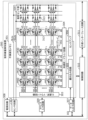
- FIG. 2 is a block diagram showing an example of the configuration of the radiation dose detection device 300 according to the embodiment.
- the radiation dose detection device 300 according to the present embodiment is composed of a semiconductor integrated circuit, and includes a nonvolatile memory 301 on a semiconductor substrate.
- This nonvolatile memory 301 includes a memory array 302 composed of memory cells M00 to Mxy arranged two-dimensionally, a row selection/driver circuit 303, a column selection/driver circuit 304, and a memory array 302 for writing information.
- the amount of current flowing through the write circuit 305 and the selected memory cells M00 to Mxy through the selected bit line is detected, and the information stored in the selected memory cells M00 to Mxy is determined as data "1" or " 0'', and a data input/output circuit 307 that performs input/output processing of input/output data via a signal node DQ.
- the radiation dose detection device 300 also has a power supply circuit 308 that generates various power supplies used inside the memory from an external power supply, an address input circuit 309 that outputs address signals to the nonvolatile memory 301, and the outside of the device. It includes an external interface circuit 311 that transmits and receives address signals, data, and control signals, and a control circuit 310 that controls the entire radiation dose detection device 300 based on signals input and output via the external interface circuit 311.
- the control circuit 310 includes, for example, a memory that stores a control program, a processor that executes the control program, and the like.
- the radiation dose detection device 300 is created using a part of the memory array 302, and includes a temperature sensor unit 320 that senses the ambient temperature, and outputs data correlated with the temperature using the temperature sensor unit 320.
- a sensor circuit 312 is provided.
- the temperature sensor section 320 has the structure and circuit configuration shown in FIGS. 1(c) and 1(d).
- the sensor circuit 312 also has a radiation dose detection function, which will be described later.
- the memory array 302 includes a plurality of word lines WL0, WL1,...WLy formed on a semiconductor substrate, bit lines BL0, BL1,...BLx arranged to cross a plurality of word lines WL0, WL1,...WLy arranged parallel to each other, and a source.
- a plurality of transistors T00, T01, ..., Txy (hereinafter referred to as “transistors T00, T01, ") provided corresponding to the intersections with the lines SL0, SL1, ...SLx, respectively, and a transistor T00. , T01,... and variable resistance elements 313 provided one-to-one are connected in series (hereinafter referred to as "memory cells M00, M01,!). ”).
- Each of the memory cells M00 to Mxy has the structure shown in FIG. 1(a), and the circuit diagram markings thereof are in accordance with FIG. 1(b).
- the variable resistance element 313 operates as a nonvolatile memory element within the memory cells M00 to Mxy.
- Each of such memory cells M00 to Mxy is composed of one selection transistor 319 and one resistance change element 313, and is therefore called a 1T1R type memory cell.
- the column selection/driver circuit 304 selects one bit line (BL) and one source line (SL), and the row selection/driver circuit 303 selects one word line, the selected bit line and source line , one memory cell intersected by the word line is selected. That is, one memory cell is selected from memory array 302. Note that although the configuration of the nonvolatile memory 301 shown in FIG. 2 is such that one memory cell is selected, it is easy to change the configuration so that multiple memory cells can be accessed simultaneously by arranging circuits in parallel. This is a design matter.
- FIG. 3 is a graph showing an example of the resistance value range of the resistance change elements 313 included in the memory cells M00 to Mxy shown in FIG. 2.
- the variable resistance elements 313 included in the memory cells M00 to Mxy have at least two states: a variable state and an initial state.
- the variable state refers to a state in which the resistance value can reversibly transition between variable resistance ranges by applying different electrical signals.
- the initial state refers to a state in which no electrical stress is applied to the variable resistance element 313 after the completion of the semiconductor manufacturing process, and an initial state where the resistance value is high and does not overlap with any of the variable resistance ranges. A state in which the resistance value is within the range.
- variable resistance element 313 in the initial state does not become variable unless forming stress, which is an electrical stress that changes it to the variable state, is applied.
- forming stress may be cumulative electrical stress. In that case, when the cumulative amount of stress exceeds a predetermined amount, the initial state transitions to the variable state.
- the memory array 302 in FIG. 2 can be made variable by individually selecting all the memory cells M00 to Mxy and applying forming stress to the variable resistance element 313 included in the selected memory cell. state, store desired data, and read the stored data as needed.
- the resistance change element 313 included in the temperature sensor section 320 is maintained in its initial state.
- the resistance change element 313 included in the temperature sensor section 320 has the configuration shown in FIGS. 1(c) and 1(d). That is, the drain of the selection transistor 319 has no plug layer 317, is not connected to the variable resistance element 313, and is grounded (grounding is not shown). The source of the selection transistor 319 is not connected to the source line but is grounded (grounding is not shown). All the plurality of variable resistance elements 313 included in the temperature sensor section 320 are connected in parallel between the temperature sensor source line SLts and the temperature sensor bit line BLts.
- FIG. 4 is a graph showing an example of the temperature characteristics of the resistance change element 313 in an initial state that constitutes the temperature sensor section 320 included in the radiation dose detection device 300 according to the embodiment. Good resistance changes are shown with respect to temperature changes.
- the plurality of resistance change elements 313 in the initial state are connected in parallel between the temperature sensor bit line BLts and the temperature sensor source line SLts.
- the resistance value between the source line SLts and the source line SLts is the combined resistance of the plurality of variable resistance elements 313 in the initial state.
- FIG. 5 is a block diagram showing the circuit configuration of the sensor circuit 312 in FIG. 2.
- the detailed circuit configuration of the power supply circuit 308 and the temperature sensor section 320 are also shown in order to show the relationship with peripheral circuits.
- a power supply circuit 308 shown in FIG. 5 includes a bandgap reference circuit BGR that generates an adjustable reference voltage Vref, and a regulator circuit 308a that outputs a power supply voltage Vreg in accordance with the reference voltage Vref.
- Regulator circuit 308a includes an operational amplifier 308b, a transistor 308c, and resistance elements R1 and R2.
- the operational amplifier 308b compares the reference voltage Vref output by the bandgap reference circuit BGR with the voltage divided by the resistors R1 and R2, and adjusts the voltage level at the gate of the transistor 308c so that these voltages become equal. adjust.
- the input voltage Vin input to the transistor 308c is a voltage higher than the output power supply voltage Vreg by more than the drop voltage caused by the transistor 308c.
- the reference voltage Vref output by the bandgap reference circuit BGR is calibrated by the adjustment voltage Vtrim input from the control circuit 310.
- the calibration value of the adjustment voltage Vtrim is determined by inspection before shipping, and is stored in the memory array 302. Therefore, the control circuit 310 reads the calibration value stored in the memory array 302 and outputs it to the bandgap reference circuit BGR as the adjustment voltage Vtrim, so that the reference voltage Vref and power supply voltage Vreg are always calibrated within a predetermined range. is output.
- the bandgap reference circuit BGR is a well-known technology, and detailed circuit configuration and explanation will be omitted. Note that in a wireless communication device such as an RF tag, a DC voltage obtained by rectifying an AC voltage generated in a communication antenna by a rectifier circuit is input to the power supply circuit 308 as an input voltage Vin.
- the temperature sensor section 320 is a temperature sensor that functions as a first current source that outputs a first current that depends on the ambient temperature of the radiation dose detection device 300 using the power supply voltage Vreg, and is shown in (c) of FIG.
- the power supply voltage Vreg is applied to the first node 320a, and the second node 320b outputs the first current.
- the temperature sensor section 320 is configured by connecting a plurality of variable resistance elements 313 in parallel, and the combined resistance is obtained by averaging the variations in resistance value of each of the plurality of variable resistance elements 313. value.
- the temperature sensor section 320 may be configured with one resistance change element 313.
- the sensor circuit 312 includes a radiation sensor unit 340 that functions as a second current source that outputs a second current that depends on the radiation dose with which the radiation dose detection device 300 is irradiated, and a radiation sensor unit 340 that uses the power supply voltage Vreg to output a second current that depends on the radiation dose irradiated with the radiation dose detection device 300. and a detection circuit 350 that outputs a first signal indicating the temperature corresponding to the magnitude of the current and a second signal indicating the radiation dose corresponding to the magnitude of the second current.
- the radiation sensor section 340 includes a transistor TRsp such as a p-type MOS transistor whose threshold voltage VT changes depending on the irradiated radiation dose, a resistance element R4 connected between the source and gate of the transistor TRsp, and a transistor TRsp.
- the resistor element R3 is connected between the gate of the resistor R3 and the ground.
- the power supply voltage Vreg is applied to one terminal (source terminal) of the transistor TRsp, and the other terminal (drain terminal) of the transistor TRsp outputs a second current.
- the detection circuit 350 includes a selection circuit 345 having two switch elements 343 and 344 that are exclusively short-circuited in order to select one of the first current and the second current and output it as a third current as a power supply current Iro.
- the ring oscillator 341 receives the power supply current Iro output from the selection circuit 345 and outputs a clock with a frequency corresponding to the power supply current Iro, and the clock output from the ring oscillator 341 is counted for a predetermined period of time.
- the counter circuit 342 outputs the counted value as a first signal or a second signal.
- the oscillation frequency of the ring oscillator 341 changes depending on the amount of power supply current Iro supplied to the ring oscillator 341.
- the output of the ring oscillator 341 is input to the counter circuit 342 as an operating clock, and when the Reset signal input from the control circuit 310 is H, the count value is reset to zero, and the Enable signal input from the control circuit 310 is H.
- the number of clocks is counted according to the input clock.
- the period during which the Enable signal is high has a certain pulse width, and is designed so that the oscillation frequency of the ring oscillator 341 can be determined from the count value Dat output from the counter circuit 342.
- the count value Dat output by the counter circuit 342 is input to the control circuit 310 and output to the outside of the radiation dose detection device 300.
- the power supply current Iro is supplied from the power supply voltage Vreg via the combined resistance of the plurality of variable resistance elements 313 forming the temperature sensor section 320. Since the combined resistance of the temperature sensor section 320 has good temperature characteristics as shown in FIG. 4, it is possible to obtain a count value Dat corresponding to the ambient temperature.
- the drain-source current determined by the gate voltage Vpg and threshold voltage VT of the transistor TRsp becomes the power supply current Iro
- the power supply current Iro becomes the ring oscillator 341 supplied to
- the oscillation frequency of the ring oscillator 341 changes. This change in oscillation frequency is obtained as a change in the count value Dat obtained from the counter circuit 342, and the degree of exposure to radiation can be quantitatively obtained. Note that the change in the threshold voltage VT of the transistor TRsp due to exposure to radiation is maintained even after the exposure to radiation ends.
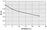
- FIG. 6 is a diagram showing an example of a measurement result obtained by measuring the ambient temperature using the temperature sensor section 320 and the sensor circuit 312 included in the radiation dose detection device 300 according to the embodiment.
- the graph in FIG. 6A shows temperature characteristics in which the horizontal axis is temperature and the vertical axis is a value obtained by converting the count value Dat obtained from the counter circuit 342 into frequency.
- (a) in FIG. 6 shows the initial temperature characteristics before exposing the radiation dose detection device 300 to radiation (dotted line of “0 KGy”) and the temperature characteristics after exposing the radiation dose detection device 300 to a radiation dose of 25 KGy.
- the measured temperature characteristics (solid line of "25 KGy”) are shown.
- the graph in FIG. 6(b) shows radiation dose-dependent characteristics with the horizontal axis representing the amount of radiation exposure and the vertical axis representing the frequency. As can be seen from FIG. 6(b), it is shown that the frequency of each temperature is almost constant. Note that the graphs shown in FIGS. 6(a) and 6(b) show measurement results obtained by adjusting the reference voltage Vref so that the power supply voltage Vreg becomes equal before and after radiation irradiation. ing.
- the parallel combined resistance of the temperature sensor section 320 exhibits favorable changes depending on temperature, and its temperature characteristics are hardly affected by radiation exposure.
- the radiation dose detection device 300 according to the present embodiment utilizes this fact, and can function as a good radiation-resistant temperature sensor without degrading detection accuracy against radiation exposure.
- the semiconductor integrated circuit that constitutes the radiation dose detection device 300 is an assembly of circuits made up of transistors, the threshold voltage VT changes due to exposure to radiation, causing fluctuations in circuit operation.
- the reference voltage Vref output by the bandgap reference circuit BGR is important because it serves as a reference for all built-in analog circuits.
- the radiation dose detection device 300 uses the temperature sensor section 320 whose temperature characteristics hardly change due to radiation exposure, so that the radiation dose of the radiation dose detection device 300 due to radiation exposure is reduced. Equipped with a calibration function that responds to changes in detection characteristics (returns to original characteristics). Calibration performed after radiation exposure will be described below.
- FIG. 7 is a flowchart showing the procedure of a radiation dose detection method including a calibration function by the radiation dose detection device 300 according to the embodiment.
- the adjustment voltage Vtrim is adjusted so that the power supply voltage Vreg shown in FIG. ing.
- the value of the adjusted voltage Vtrim adjusted at this time is set as a value Vtrim0, and the values of the obtained reference voltage Vref and power supply voltage Vreg are set as a value Vref0 and a value Vreg0, respectively.
- temperature characteristics are measured using the temperature sensor section 320 and the sensor circuit 312 under the power supply voltage Vreg of value Vreg0, and the measurement results are stored in the memory array 302 of the nonvolatile memory 301 (S10). More specifically, the control circuit 310 stores in the memory array 302, for example, a count value C25 obtained from the counter circuit 342 of the sensor circuit 312 at a room temperature of 25 degrees and a count value C85 at a temperature of 85 degrees. If the relationship between the temperature at two points and the count value is known, a characteristic function of temperature characteristics as shown in FIG. 4 can be derived, and the ambient temperature can be monitored from the obtained count value.
- the selection circuit 345 selects the first current, and the first correlation between the ambient temperature and the count value output by the counter circuit 342 is calculated before the radiation irradiation. This corresponds to a first acquisition step of acquiring (that is, the temperature characteristics of the temperature sensor section 320).
- control circuit 310 also acquires the already stored temperature characteristics of the radiation sensor section 340 from the memory array 302 of the nonvolatile memory 301 (S11). For example, a function indicating how the measured radiation dose should be corrected depending on the ambient temperature, that is, a function indicating the temperature dependence of the measured radiation dose is obtained.
- This step S11 corresponds to a third acquisition step of acquiring a third correlation indicating the temperature dependence of the count value output by the counter circuit 342 while the selection circuit 345 selects the second current.
- the radiation dose detection device 300 is exposed to radiation for sterilization and the like (S12). After exposure to radiation, the power supply voltage Vreg adjusted by the trimming value Vtrim0 changes due to the influence of the radiation and is no longer the voltage Vreg0.
- step S10 the radiation dose detection device 300 to be calibrated stores the count value C25 and the count value C85 in the memory array 302 before shipping, so the control circuit 310 stores the count value C25 and the count value C85.
- the control circuit 310 By reading out and count value C85 from the memory array 302, a function indicating temperature characteristics is obtained.
- An expected count value Ct corresponding to the current temperature Tc is calculated from the obtained temperature characteristic function.
- step S13 after radiation irradiation, the control circuit 310 obtains a second correlation between the ambient temperature and the count value output by the counter circuit 342 while the selection circuit 345 selects the first current.
- step S14 corresponds to an adjustment step in which the control circuit 310 adjusts the reference voltage so that the first correlation and the second correlation are equal.
- the value Vreg1 will be equal to the value Vreg0 before radiation exposure.
- the calibrated Vtrim value is stored in memory array 302, thereby updating the trim value.
- the control circuit 310 short-circuits only the switch element 344 in the selection circuit 345, operates the radiation sensor section 340, and obtains a count value, thereby calculating the radiation dose (S15).
- This step S15 corresponds to a radiation dose detection step in which the selection circuit 345 selects the second current under the control of the control circuit 310 and detects the radiation dose.
- control circuit 310 uses the temperature characteristics of the radiation sensor unit 340 acquired in step S11 to calculate the radiation dose after temperature correction from the current temperature Tc and the radiation dose obtained in step S15. (S16).
- the temperature characteristics of the temperature sensor section 320 can be adjusted by calibrating the power supply voltage Vreg after radiation exposure to the same voltage as before exposure. are the same before and after radiation irradiation as shown in FIG. Provided as a temperature sensor.
- the above-mentioned power supply voltage is calibrated after exposure to radiation, and the ring oscillator 341 is operated by the power supply current Iro supplied by the radiation sensor section 340 while the power supply voltage Vreg is kept constant, and the counter By obtaining the count value in the circuit 342, it is possible to accurately monitor the amount of radiation exposure that is not affected by radiation exposure.
- step S11 may be performed at any stage before step S16. Further, in step S10, if the obtained first correlation is stored in the memory array 302, the first correlation may be acquired at any stage before step S14. .
- FIG. 8 shows an example of the relationship between the radiation dose irradiated to the radiation dose detection device 300 according to the embodiment (horizontal axis) and the frequency change rate (vertical axis) based on the obtained count value. It is a diagram. Here, the results are obtained by implementing the calibration method shown in FIG. 7. Note that the rate of change on the vertical axis is the rate of change in the measured frequency when the initial frequency before exposure to radiation is set to 1. Because each radiation dose detection device is affected by individual variations due to circuit process variations, etc., the frequency varies, so by using the rate of change instead of frequency, the radiation dose can be measured without depending on the radiation dose detection device. can be monitored. As can be seen from FIG.
- the frequency decreases with a negative correlation with the irradiated radiation dose. Utilizing this characteristic, the count value output from the counter circuit 342 reveals an accurate amount of radiation exposure that is hardly affected by radiation exposure.
- the radiation dose detection device 300 uses the power supply circuit 308 that outputs the power supply voltage Vreg and the first current that depends on the ambient temperature of the radiation dose detection device 300 using the power supply voltage Vreg.
- the radiation dose detection device 300 functions as a second current source that outputs a second current depending on the irradiated radiation dose using the temperature sensor section 320 that functions as a first current source that outputs the radiation dose and the power supply voltage Vreg. It includes a radiation sensor section 340 and a detection circuit 350 that outputs a first signal indicating the temperature corresponding to the magnitude of the first current and a second signal indicating the radiation dose corresponding to the magnitude of the second current.
- the temperature sensor section 320 includes a first electrode layer 316, a second electrode layer 314, and a variable resistance layer 315 containing a transition metal oxide interposed between the first electrode layer 316 and the second electrode layer 314.
- a second node 320b is connected to each other, the power supply voltage Vreg is applied to the first node 320a, the second node 320b outputs the first current, and the second current source is connected to the transistor TRsp.
- a power supply voltage Vreg is applied to one terminal of the transistor TRsp, and the other terminal of the transistor TRsp outputs a second current.
- the radiation dose detection device 300 not only enables the temperature sensor section 320 to detect temperature, but also allows the temperature sensor section 320 to be a resistor containing a transition metal oxide that is hardly affected by radiation exposure. By utilizing the characteristic of being composed of variable elements, it becomes possible to respond to changes in the characteristics of the radiation dose detection device due to radiation exposure.
- the transition metal oxide is, for example, at least one of aluminum oxide, tantalum oxide, hafnium oxide, and zirconium oxide.
- the radiation dose detection device 300 includes a resistance change type nonvolatile memory 301 in which a plurality of resistance change elements 313 are arranged in an array, and one or more resistance change elements 313 included in the temperature sensor section 320 are nonvolatile memory This is a part of a plurality of resistance change elements 313 that constitute 301.
- one or more resistance change elements 313 included in the temperature sensor section 320 are configured as a part of the plurality of resistance change elements 313 that constitute the nonvolatile memory 301, so that the temperature sensor section 320 can be and nonvolatile memory 301 can be manufactured.
- dummy cells that are not used for data storage are generally arranged at the outer periphery of the array in order to ensure processing uniformity in the manufacturing process. Therefore, by using the dummy cell in the temperature sensor section 320, there is no need to add a separate cell for this device, and the circuit area can be used effectively.
- the detection circuit 350 also receives a selection circuit 345 that selects one of the first current and the second current and outputs it as a third current, and a third current output from the selection circuit 345, and outputs the third current as the third current.
- a ring oscillator 341 that outputs a clock of a corresponding frequency
- a counter circuit 342 that counts the clock output from the ring oscillator 341 for a predetermined period of time and outputs the obtained count value as a first signal or a second signal. have This allows the common detection circuit 350 to measure the first current and the second current, thereby reducing the circuit scale.
- the power supply circuit 308 includes a bandgap reference circuit BGR that generates an adjustable reference voltage Vref, and a regulator circuit 308a that outputs a power supply voltage Vreg in accordance with the reference voltage Vref.
- a bandgap reference circuit BGR that generates an adjustable reference voltage Vref
- a regulator circuit 308a that outputs a power supply voltage Vreg in accordance with the reference voltage Vref.
- the radiation dose detection device 300 further calculates the first count value output by the counter circuit 342 before radiation irradiation, the first ambient temperature when the first count value is output, and the counter circuit 342 after radiation irradiation. From the second count value output by the circuit 342 and the second ambient temperature at the time the second count value is output, a first correlation between the first count value and the first ambient temperature and a second count value are determined.
- a control circuit 310 is provided that adjusts the reference voltage Vref so that the second correlation with the second ambient temperature is equal. Thereby, by adjusting the reference voltage Vref so as to match the temperature characteristics of the temperature sensor section 320 before and after radiation exposure, the same power supply voltage Vreg can be maintained before and after radiation exposure.
- the radiation dose detection method is a radiation dose detection method using the radiation dose detection device 300, in which the selection circuit 345 selects the first current and the ambient temperature is adjusted before radiation irradiation.
- the radiation dose detection method further includes a third acquisition step of acquiring a third correlation indicating the temperature dependence of the count value output by the counter circuit 342 while the selection circuit 345 selects the second current;
- the third correlation is used to calculate the temperature-corrected radiation dose from the count value output by the counter circuit 342 obtained by detecting the radiation dose.
- the temperature dependence of the radiation sensor section 340 is corrected, and a radiation dose after temperature correction is obtained.
- the present disclosure is not limited to the embodiments.
- the scope of the present disclosure also includes various modifications that can be thought of by those skilled in the art to the present embodiment, and other forms constructed by combining some of the constituent elements of the embodiments, as long as they do not depart from the spirit of the present disclosure. contained within.
- the detection circuit 350 includes the ring oscillator 341, but it does not necessarily need to include such a configuration.
- the detection circuit 350 may be a circuit configured with a current-voltage converter and an A/D converter, etc., as long as it outputs a digital value that depends on the power supply current Iro output from the temperature sensor section 320 or the radiation sensor section 340. It may also be configured with other circuits.
- the power supply circuit 308 has a function of adjusting the power supply voltage Vreg, but a circuit for adjusting the power supply voltage Vreg output from the power supply circuit 308 may be provided outside the power supply circuit 308. .
- the radiation dose detection device is used as a sensor that maintains good temperature and radiation dose sensing accuracy even after exposure to radiation, and is used as a sensor that is configured of, for example, a semiconductor integrated circuit device and whose life cycle is managed; Alternatively, it is subjected to radiation sterilization while still attached to the packaging material containing it, and by calibrating the circuit operating voltage using RF communication, it is possible to manage the life cycle of the object without deteriorating sensing accuracy. It can be used as an RFID tag. That is, since it can be used as an RFID that excludes the influence of radiation, it is possible to save the effort of attaching and detaching an RFID tag attached to an object whose life cycle is to be managed before and after radiation irradiation.
- Nonvolatile memory 302 Memory array 303 Row selection/driver circuit 304 Column selection/driver circuit 305 Write circuit 306 Sense amplifier 307 Data input/output circuit 308 Power supply circuit 308a Regulator circuit 308b Operational amplifier 308c Transistor 309 Address input circuit 310 Control circuit 311 External interface circuit 312 Sensor circuit 313 Resistance change element 314 Second electrode layer 315 Variable resistance layer 315a Second tantalum oxide layer 315b First tantalum oxide layer 316 First electrode layer 317 Plug layer 318 Metal wiring Layer 319 Selection transistor 320 Temperature sensor section 320a First node 320b Second node 340 Radiation sensor section 341 Ring oscillator 342 Counter circuit 343, 344 Switch element 345 Selection circuit 350 Detection circuit BGR Band gap reference circuit BL0 to BLx Bit line BLts Temperature sensor Bit line for M00 ⁇ Mxy Memory cell SL0 ⁇ SLx Source line SLts Source line for temperature sensor T00 ⁇ Txy, TRsp
Abstract
放射線量検知装置(300)は、電源電圧(Vreg)を出力する電源回路(308)と、電源電圧(Vreg)を用いて周囲温度に依存する第1電流を出力する第1電流源として機能する温度センサ部(320)と、電源電圧(Vreg)を用いて放射線量検知装置(300)が照射された放射線量に依存する第2電流を出力する第2電流源として機能する放射線センサ部(340)と、第1電流の大きさに対応する温度を示す第1信号を出力し、第2電流の大きさに対応する放射線量を示す第2信号を出力する検知回路(350)とを備え、温度センサ部(320)は、遷移金属酸化物を含む可変抵抗層(315)を有する1つ以上の抵抗変化素子(313)を有し、第2電流源は、トランジスタ(TRsp)を有する。
Description
本開示は、放射線量検知装置および放射線量検知方法に関し、より詳しくは放射線への曝露による特性変化への対応を可能にする機能をもつ放射線量検知装置に関する。
ガンマ線などの放射線はマイクロエレクトロニクスに有害な影響を及ぼすおそれがある。長年の研究により、放射線がマイクロエレクトロニクスに及ぼす様々な影響が明らかにされており、これらの影響がマイクロエレクトロニクスの正常な動作・機能に対して問題を引き起こすことが指摘されている。放射線への曝露により集積回路内には一時的な障害と不可逆な固定的障害が生じる。前者はフリップフロップやRAM(ランダムアクセスメモリ)などのデータの論理反転といったソフトエラー(シングルイベント効果ともいう)であらわされ、後者はトランジスタのオン電圧(言い換えると、閾値電圧VT)のシフトやリーク電流の増加が代表的である。
例えば、医療機器や医薬品容器、更に香辛料といった食料品は、放射線による滅菌処理がなされる。そういった製品や梱包材にRFタグを付加し、製品の在庫管理やトレーサビリティーを確保するためには放射線照射後にもRFタグが正常に動作する必要がある。
また、特許文献1で例示されているようにRFタグに放射線センサや温度センサなどのセンシング機能があれば、そのセンシング精度も所定の性能を維持することが求められる。しかしながら、一般に半導体集積回路では、外部から入力される電源電圧から集積回路内の動作電圧を生成するためレギュレータ回路が設けられている。そして、レギュレータ回路が所定の電圧を生成するために、その基準となる基準電圧を生成するバンドギャップレファレンス回路が搭載される。レギュレータ回路およびバンドギャップレファレンス回路は周知の技術であるので、ここでは詳細な説明は省略する。
通常、バンドギャップレファレンス回路が生成するレファレンス電圧のバラツキは、RFタグの出荷前検査によりトリミング調整がなされ、所望な電圧が出力するように処置される。これによりレギュレータ回路が出力する電源電圧も所定の範囲の電圧に調整される。そして、前述したような所定の範囲に調整された電源電圧下のもとで、同様にセンサ素子を搭載したRFタグは、製造後の検査でセンシング動作の校正が実施される。例えば温度センサであれば、全てのRFタグが所定の範囲に調整された電源電圧下においてセンサ素子から得られる物理量と温度との関係性(つまり、温度特性)を校正し、得られた物理量から正確な温度が対応するようにする。
しかし、出荷後のフィールドにおいて放射線への曝露によりトランジスタの閾値電圧VTが変化すると、基準電圧が、曝露前に比べ変化し、それにともなって生成される電源電圧が変化してしまう。これにより、放射線照射後に動作する電源電圧が校正時と異なればセンサ素子から得られる物理量と温度との関係性が変わり正確な温度が得られなくなってしまう。このことは放射線センサ素子を用いた放射線検知回路でも同様である。そして、更に高い放射線量に曝露し、閾値電圧VTのシフトが大きくなり電源電圧がタグの正常動作限界を超えて変動した場合にはRFタグ自体の動作に異常をきたしてしまう。
例えば半導体集積回路が放射線に曝露したときに回路に与える影響をモニタし曝露量を計測する方法が特許文献2に例示されている。特許文献2では、半導体集積回路に搭載されたリングオシレータが発生するパルスの周波数が、放射線への曝露量に応じて変化することを利用して曝露量をモニタすることが提案されている。そして、特許文献3では、抵抗変化素子が温度によって抵抗値が変化する特性を活かし、その抵抗をもとにしたオシレータの発振周波数が温度により変化することで半導体集積回路の周囲温度をモニタすることが提案されている。
しかしながら、特許文献1~3が提案する装置は、前述したような放射線への曝露による電源電圧変動に対して影響を受け、そのセンシング精度が低下してしまうという問題に対応できていない。つまり、前述の先行例のように、RFタグを用いて、温度や放射線、更に別の周囲環境をセンシングし情報収集することが提案されているものの、半導体集積回路が放射線に曝露すると、集積回路を構成するトランジスタが不可逆的なダメージを受け、電源電圧が初期から変動し、正常なセンシングができない、または精度が劣化するといった課題がある。
そこで、本開示は、放射線量だけでなく温度も検知し、かつ、放射線への曝露による特性変化への対応を可能にする機能をもつ放射線量検知装置、および、そのような放射線量検知装置による放射線量検知方法を提供することを目的とする。
上記目的を達成するために、本開示の一形態に係る放射線量検知装置は、電源電圧を出力する電源回路と、前記電源電圧を用いて、前記放射線量検知装置の周囲温度に依存する第1電流を出力する第1電流源と、前記電源電圧を用いて、前記放射線量検知装置が照射された放射線量に依存する第2電流を出力する第2電流源と、前記第1電流の大きさに対応する温度を示す第1信号を出力し、前記第2電流の大きさに対応する放射線量を示す第2信号を出力する検知回路とを備え、前記第1電流源は、第1電極層、第2電極層、および、前記第1電極層と前記第2電極層との間に介在する遷移金属酸化物を含む可変抵抗層を有する1つ以上の抵抗変化素子と、前記1つ以上の抵抗変化素子の前記第1電極層どうしを接続している第1ノードと、前記1つ以上の抵抗変化素子の前記第2電極層どうしを接続している第2ノードとを有し、前記第1ノードには、前記電源電圧が印加され、前記第2ノードは、前記第1電流を出力し、前記第2電流源は、トランジスタを有し、前記トランジスタの一端子には、前記電源電圧が印加され、前記トランジスタの他の一端子は、前記第2電流を出力する。
また、上記目的を達成するために、本開示の一形態に係る放射線量検知方法は、上記放射線量検知装置による放射線量検知方法であって、放射線の照射前に、前記選択回路が前記第1電流を選択した状態で、前記周囲温度と前記カウンタ回路が出力するカウント値との第1相関関係を取得する第1取得ステップと、放射線の照射後に、前記選択回路が前記第1電流を選択した状態で、前記周囲温度と前記カウンタ回路が出力するカウント値との第2相関関係を取得する第2取得ステップと、前記第1相関関係と前記第2相関関係とが等しくなるように、前記レファレンス電圧を調整する調整ステップと、前記調整ステップの後に、前記選択回路が前記第2電流を選択した状態で、放射線量を検知する放射線量検知ステップとを含む。
本開示により、放射線量だけでなく温度も検知し、かつ、放射線への曝露による特性変化への対応を可能にする機能をもつ放射線量検知装置、および、そのような放射線量検知装置による放射線量検知方法が提供される。
(発明者らが得た知見)
本願の発明者らは種々の研究において遷移金属を用いた抵抗変化素子に用いられる遷移金属酸化物が良好な温度変化特性を備えつつ、放射線曝露に対してほとんど影響を受けないことを見出した。よって、放射線量検知装置に、遷移金属酸化物を含む抵抗変化素子を内蔵させることで、放射線曝露後において、放射線量検知装置における電源電圧を放射線曝露前の値に復帰させる(つまり、校正する)ことが可能になる。よって、遷移金属酸化物を含む抵抗変化素子を備える放射線量検知装置にすることで、放射線量に加えて温度も検知できるだけでなく、放射線曝露による放射線量検知装置の特性変化に対応することが可能になる、つまり、放射線耐性をもつ温度検知と放射線量検知とが可能になるという知見を得るに至った。
本願の発明者らは種々の研究において遷移金属を用いた抵抗変化素子に用いられる遷移金属酸化物が良好な温度変化特性を備えつつ、放射線曝露に対してほとんど影響を受けないことを見出した。よって、放射線量検知装置に、遷移金属酸化物を含む抵抗変化素子を内蔵させることで、放射線曝露後において、放射線量検知装置における電源電圧を放射線曝露前の値に復帰させる(つまり、校正する)ことが可能になる。よって、遷移金属酸化物を含む抵抗変化素子を備える放射線量検知装置にすることで、放射線量に加えて温度も検知できるだけでなく、放射線曝露による放射線量検知装置の特性変化に対応することが可能になる、つまり、放射線耐性をもつ温度検知と放射線量検知とが可能になるという知見を得るに至った。
(実施の形態)
以下、本開示の実施の形態について、図面を用いて詳細に説明する。なお、以下で説明する実施の形態は、いずれも本開示の一具体例を示す。以下の実施の形態で示される数値、形状、材料、構成要素、構成要素の配置位置及び接続形態、ステップ、ステップの順序等は、一例であり、本開示を限定する主旨ではない。また、各図は、必ずしも厳密に図示したものではない。各図において、実質的に同一の構成については同一の符号を付し、重複する説明は省略又は簡略化する。また、「接続」とは、電気的な接続を意味し、2つの回路要素が直接的に接続される場合だけでなく、2つの回路要素の間に他の回路要素を挿入した状態で2つの回路要素が間接的に接続される場合も含まれる。また、Aの「上に」とは、Aに接する場合と、接しない場合とが含まれ得る。
以下、本開示の実施の形態について、図面を用いて詳細に説明する。なお、以下で説明する実施の形態は、いずれも本開示の一具体例を示す。以下の実施の形態で示される数値、形状、材料、構成要素、構成要素の配置位置及び接続形態、ステップ、ステップの順序等は、一例であり、本開示を限定する主旨ではない。また、各図は、必ずしも厳密に図示したものではない。各図において、実質的に同一の構成については同一の符号を付し、重複する説明は省略又は簡略化する。また、「接続」とは、電気的な接続を意味し、2つの回路要素が直接的に接続される場合だけでなく、2つの回路要素の間に他の回路要素を挿入した状態で2つの回路要素が間接的に接続される場合も含まれる。また、Aの「上に」とは、Aに接する場合と、接しない場合とが含まれ得る。
はじめに、本開示に係る放射線量検知装置に適用する抵抗変化素子の代表例とともに、温度センサへの適用方法について説明する。
(抵抗変化素子)
図1は、実施の形態に係る放射線量検知装置が備える抵抗変化素子の構造を示す図である。図1の(a)は、抵抗変化素子を用いたメモリセルの断面図である。半導体基板上にソース/ドレイン領域が配置され、メモリセルの選択に用いられる選択トランジスタ319が形成されている。図1の(a)において、BL0は0番目のビット線を示し、WL0,WL1は夫々ワード線の0番目と1番目を示し、SL0はソース線の0番目を示す。図1の(a)からワード線とビット線、ソース線が、異なる配線層を用いて直行するように交差していることがわかる。また、図1の(a)には、プラグ層317、および、金属配線層318もそれぞれ示されている。ここで、情報を記憶するのに使用する不揮発性記憶素子は、電気的ストレスを加える電圧とその方向(極性)によって抵抗値が変化する抵抗変化素子313である。
図1は、実施の形態に係る放射線量検知装置が備える抵抗変化素子の構造を示す図である。図1の(a)は、抵抗変化素子を用いたメモリセルの断面図である。半導体基板上にソース/ドレイン領域が配置され、メモリセルの選択に用いられる選択トランジスタ319が形成されている。図1の(a)において、BL0は0番目のビット線を示し、WL0,WL1は夫々ワード線の0番目と1番目を示し、SL0はソース線の0番目を示す。図1の(a)からワード線とビット線、ソース線が、異なる配線層を用いて直行するように交差していることがわかる。また、図1の(a)には、プラグ層317、および、金属配線層318もそれぞれ示されている。ここで、情報を記憶するのに使用する不揮発性記憶素子は、電気的ストレスを加える電圧とその方向(極性)によって抵抗値が変化する抵抗変化素子313である。
図1の(a)に示すように、抵抗変化素子313は、下層から2層目の金属配線層318と3層目の金属配線層318との間に形成される。なお、抵抗変化素子313が配置される層間位置は2-3層間に限定されず、プロセス上の都合により変更しても良い。図1の(a)に示す抵抗変化素子313は2層目の金属配線層318上に形成された第1電極層316と、第2電極層314と、第1電極層316および第2電極層314に挟まれた可変抵抗層315とを備えている。本実施の形態では、一例として可変抵抗層315が、酸素含有率が低い第1のタンタル酸化物層315b(以下、「第1のタンタル酸化物層」または単に「第1の酸化物層」ともいう)と、その第1のタンタル酸化物層315b上に形成された酸素含有率が高い第2のタンタル酸化物層315a(以下、「第2のタンタル酸化物層」または単に「第2の酸化物層」ともいう)とで構成されている。
なお、可変抵抗層315は酸素欠損型抵抗変化材料であって酸素含有率が異なる2層から構成されれば良いので、そのベースの材料がタンタルに限定されるものでない。その他の可変抵抗層315を構成する金属としては、遷移金属、およびアルミニウム(Al)の少なくともいずれかを用いることができる。遷移金属としては、タンタル(Ta)、チタン(Ti)、ハフニウム(Hf)、ジルコニウム(Zr)、ニオブ(Nb)、タングステン(W)、ニッケル(Ni)、鉄(Fe)等を用いることができる。遷移金属は複数の酸化状態をとることができるため、異なる抵抗状態を酸化還元反応により実現することが可能である。
この抵抗変化素子313を駆動する場合、外部の電源をもとにして生成される所定の条件を満たす電圧を第1電極層316と第2電極層314との間に印加する。電圧印加の方向(つまり、極性)に従い、抵抗変化素子313の可変抵抗層315の抵抗値が、可逆的に増加または減少し、少なくとも抵抗値が高い高抵抗状態(HR状態)と、高抵抗状態より抵抗値の低い低抵抗状態(LR状態)の2つ以上の状態に遷移可能である。電圧印加を停止した後も、抵抗状態が保持され、各状態に応じて情報の記録に用いることができる。
第1電極層316および第2電極層314の材料としては、例えば、Pt(白金)、Ir(イリジウム)、W(タングステン)、Cu(銅)、Al(アルミニウム)、TiN(窒化チタン)、TaN(窒化タンタル)およびTiAlN(窒化チタンアルミニウム)などがある。
図1の(a)における点線エリアが1つのメモリセルをなし、その回路図標記したものが図1の(b)である。図1の(b)からも分かるように、メモリセルでは、抵抗変化素子313と選択トランジスタ319のドレイン端子とが接続されていることが理解できる。以降において、不揮発性メモリの全体の構成要素を説明する上でメモリセルは図1の(b)の標記に従うものとする。
一方、図1の(c)は、温度センサとして用いられる抵抗変化素子313の構造を示す図である。図1の(c)は、図1の(a)に示されるメモリセルにおける抵抗変化素子313と選択トランジスタ319とが切り離された(非接続の)構造を示している。図1の(c)における点線エリアの回路図標記したものが図1の(d)である。図1の(d)からも分かるように、温度センサに用いられる抵抗変化素子313と選択トランジスタ319のドレイン端子とは、図1の(a)および(b)に示されたメモリセルと異なり、接続されていないことが理解できる。つまり、図1の(c)に示される抵抗変化素子313は、メモリセルとして機能するのではなく、温度センサとして機能する。
このように、本実施の形態に係る放射線量検知装置は、メモリセルを構成する不揮発性記憶素子としての抵抗変化素子313と、温度センサとしての抵抗変化素子313とを有する。
次に図1に示される抵抗変化素子313が用いられた不揮発性メモリを備える放射線量検知装置の一構成例を説明する。
図2は、実施の形態に係る放射線量検知装置300の一構成例を示すブロック図である。図2に示すように、本実施の形態に係る放射線量検知装置300は、半導体集積回路で構成され、半導体基板上に、不揮発性メモリ301を備えている。この不揮発性メモリ301は、2次元状に配置されたメモリセルM00~Mxyで構成されるメモリアレイ302と、行選択/ドライバ回路303と、列選択/ドライバ回路304と、情報の書き込みを行うための書き込み回路305と、選択されたビット線を介して選択されたメモリセルM00~Mxyに流れる電流量を検出し、選択されたメモリセルM00~Mxyに記憶された情報がデータ「1」または「0」のいずれであるかを判定するセンスアンプ306と、信号ノードDQを介して入出力データの入出力処理を行うデータ入出力回路307とを具備している。
また、放射線量検知装置300は、外部電源からメモリ内部で使用される各種電源を生成する電源回路308と、不揮発性メモリ301にアドレス信号を出力するアドレス入力回路309と、装置外部との間でアドレス信号、データ、コントロール信号を送受信する外部インターフェース回路311と、外部インターフェース回路311を介して入出力される信号をもとに放射線量検知装置300全体を制御する制御回路310とを備えている。なお、制御回路310は、例えば、制御プログラムを記憶するメモリ、および、制御プログラムを実行するプロセッサなどで構成される。
更に、放射線量検知装置300は、メモリアレイ302の一部を利用して作成され、周囲温度をセンシングする温度センサ部320、および、温度センサ部320を用いて温度と相関のあるデータを出力するセンサ回路312を備えている。温度センサ部320は、図1の(c)および(d)に示される構造および回路構成を備える。センサ回路312は、後述する放射線量検知機能も有している。
メモリアレイ302は、半導体基板の上に形成された、互いに平行するように配列された複数のワード線WL0,WL1,…WLyと交差するように配列されたビット線BL0,BL1,…BLxおよびソース線SL0,SL1,・・・SLxとの交点に対応してそれぞれ設けられた複数のトランジスタT00,T01,・・・,Txy(以下、「トランジスタT00,T01,…」と表す)と、トランジスタT00,T01,…と1対1に設けられた抵抗変化素子313とが直列に接続された構成を有する複数のメモリセルM00,M01,・・・,Mxy(以下、「メモリセルM00,M01,…」と表す)とを備えている。
各メモリセルM00~Mxyは、図1の(a)に示される構造を有し、その回路図標記は図1の(b)にしたがっている。このとき抵抗変化素子313はメモリセルM00~Mxy内で不揮発性記憶素子として動作する。このようなメモリセルM00~Mxyのそれぞれは、1つの選択トランジスタ319と1つの抵抗変化素子313とから構成されていることから、1T1R型メモリセルと呼ばれる。
列選択/ドライバ回路304により一本のビットライン(BL)とソースライン(SL)が選択され、行選択/ドライバ回路303が、一つのワード線を選択するとき、選択されたビット線、ソース線、ワード線が交差するメモリセルが1つ選択される。すなわち、メモリアレイ302から、1つのメモリセルが選択される。なお、図2に示した不揮発性メモリ301の構成は1つのメモリセルが選択されるものであるが、回路を並列に配置することで複数のメモリセルを同時にアクセスするように変更することは容易な設計事項である。
図3は、図2に示されるメモリセルM00~Mxyに含まれる抵抗変化素子313の抵抗値範囲の一例を示すグラフである。図3に例示するように、メモリセルM00~Mxyに含まれる抵抗変化素子313は、少なくとも可変状態と初期状態の2つの状態を備えている。可変状態とは、異なる電気的信号が印加されることによって、抵抗値が可変抵抗範囲の間を可逆的に遷移できる状態をいう。初期状態とは、半導体製造プロセスの完了後で、抵抗変化素子313に一度も電気的ストレスが印加されていない状態をさし、抵抗値が可変抵抗範囲のいずれとも重複しない、抵抗値が高い初期抵抗値範囲にある状態をいう。
初期状態にある抵抗変化素子313は、可変状態に変化させるような電気的ストレスであるフォーミングストレスが印加されない限り可変状態とならない。例えば、フォーミングストレスは累積的な電気的ストレスであってもよい。その場合、ストレスの累積量が所定量を超えたときに、初期状態から可変状態に遷移する。
図2のメモリアレイ302は、半導体製造プロセス完了後、全てのメモリセルM00~Mxyを個別に選択し、選択したメモリセルに含まれる抵抗変化素子313に対して、フォーミングストレスを印加することで可変状態に遷移させ、所望なデータを記憶し、必要に応じて記憶したデータを読み出せるようにする。
一方で、温度センサ部320に含まれる抵抗変化素子313は、初期状態のまま維持される。温度センサ部320に含まれる抵抗変化素子313は、図1の(c)および(d)に示す構成になっている。つまり、選択トランジスタ319のドレインは、プラグ層317が無く抵抗変化素子313に接続されずグランドに接地される(グランドへの接地については図示せず)。そして選択トランジスタ319のソースはソースラインに接続されずグランドに接地される(グランドへの接地については図示せず)。温度センサ部320に含まれる複数の全ての抵抗変化素子313は、温度センサ用ソースラインSLtsと温度センサ用ビットラインBLts間に並列して接続される。
図4は、実施の形態に係る放射線量検知装置300が備える温度センサ部320を構成する初期状態の抵抗変化素子313の温度特性の一例を示すグラフである。温度変化に対して良好な抵抗値変化が示されている。温度センサ部320は、複数の初期状態の抵抗変化素子313が温度センサ用ビットラインBLtsと温度センサ用ソースラインSLtsとの間に並列に接続されるため、温度センサ用ビットラインBLtsと温度センサ用ソースラインSLtsとの間の抵抗値は、初期状態にある複数の抵抗変化素子313の合成抵抗となる。
図5は、図2におけるセンサ回路312の回路構成を示すブロック図である。本図には、周辺回路との関係を示すために、電源回路308の詳細な回路構成と温度センサ部320とが併記されている。
図5に示す電源回路308は、調整可能なレファレンス電圧Vrefを生成するバンドギャップレファレンス回路BGRと、レファレンス電圧Vrefに従って、電源電圧Vregを出力するレギュレータ回路308aとを有する。レギュレータ回路308aは、演算増幅器308b、トランジスタ308c、抵抗素子R1およびR2を有する。演算増幅器308bは、バンドギャップレファレンス回路BGRが出力するレファレンス電圧Vrefと、抵抗素子R1およびR2による分圧電圧Vfbとを比較し、これらの電圧が等しくなるように、トランジスタ308cのゲートの電圧レベルを調整する。このため演算増幅器308bの-入力端子に流れ込む電流をIfbとすると、電源回路308の出力電圧である電源電圧Vregは、Vreg=Vref×(1+R2/R2)+Ifb×R2であらわされる。電流Ifdは非常に小さいため、この式の右辺は、ほぼVref×(1+R2/R2)となる。このときトランジスタ308cに入力される入力電圧Vinは、出力される電源電圧Vregよりトランジスタ308cによるドロップ電圧以上大きい電圧である。
バンドギャップレファレンス回路BGRが出力するレファレンス電圧Vrefは、制御回路310から入力される調整電圧Vtrimによって校正される。調整電圧Vtrimの校正値は、出荷前の検査によって決定されており、メモリアレイ302に格納されている。よって、制御回路310が、メモリアレイ302に格納された校正値を読み出し、調整電圧Vtrimとしてバンドギャップレファレンス回路BGRに出力することで、常に校正された所定の範囲内のレファレンス電圧Vrefと電源電圧Vregとが出力される。
バンドギャップレファレンス回路BGRは、周知の技術であり、詳細な回路構成および説明を省略する。なお、RFタグのような無線通信装置では、通信用アンテナに発生する交流電圧を整流回路により整流した直流電圧が入力電圧Vinとして電源回路308に入力される。
温度センサ部320は、電源電圧Vregを用いて、放射線量検知装置300の周囲温度に依存する第1電流を出力する第1電流源として機能する温度センサであり、図1の(c)に示される構造を有する複数の抵抗変化素子313と、複数の抵抗変化素子313の第1電極層316どうしを接続している第1ノード320aと、複数の抵抗変化素子313の第2電極層314どうしを接続している第2ノード320bとを有する。第1ノード320aには、電源電圧Vregが印加され、第2ノード320bは、第1電流を出力する。
なお、本実施の形態では、温度センサ部320が複数の抵抗変化素子313の並列接続で構成され、その合成抵抗は、複数の抵抗変化素子313のそれぞれがもつ抵抗値のばらつきが平均化された値となる。ただし、このような構成は必須ではなく、温度センサ部320が1つの抵抗変化素子313で構成されてもよい。
センサ回路312は、電源電圧Vregを用いて、放射線量検知装置300が照射された放射線量に依存する第2電流を出力する第2電流源として機能する放射線センサ部340と、第1電流の大きさに対応する温度を示す第1信号を出力し、第2電流の大きさに対応する放射線量を示す第2信号を出力する検知回路350とを備える。
放射線センサ部340は、照射された放射線量に応じて閾値電圧VTが変化するp型MOSトランジスタ等のトランジスタTRsp、トランジスタTRspのソースとゲートとの間に接続される抵抗素子R4、および、トランジスタTRspのゲートとグランドとの間に接続される抵抗素子R3を有する。トランジスタTRspの一端子(ソース端子)には、電源電圧Vregが印加され、トランジスタTRspの他の一端子(ドレイン端子)は、第2電流を出力する。
検知回路350は、第1電流および第2電流の一方を選択し、第3電流としての電源電流Iroとして出力するために、排他的にショートとなる2つのスイッチ素子343および344を有する選択回路345と、選択回路345から出力される電源電流Iroの供給を受け、電源電流Iroに応じた周波数のクロックを出力するリングオシレータ341と、リングオシレータ341が出力するクロックを所定の時間カウントし、得られたカウント値を、第1信号または第2信号として、出力するカウンタ回路342とで構成される。
より詳しくは、リングオシレータ341は、リングオシレータ341に供給される電源電流Iroの量により発振周波数が変化する。リングオシレータ341の出力は、動作クロックとしてカウンタ回路342に入力され、制御回路310から入力されるReset信号がHのとき、カウント値がゼロにリセットされ、制御回路310から入力されるEnable信号がHのとき、入力されるクロックに従いクロック数をカウントする。Enable信号がHとなる期間は、一定のパルス幅分あり、カウンタ回路342から出力されるカウント値Datからリングオシレータ341の発振周波数が判別できるように設計されている。
カウンタ回路342が出力するカウント値Datは、制御回路310に入力され、放射線量検知装置300の外に出力される。
選択回路345においてスイッチ素子343だけがショート状態の時は、電源電流Iroは、温度センサ部320を構成する複数の抵抗変化素子313の合成抵抗を介して、電源電圧Vregから供給される。温度センサ部320の合成抵抗は図4で示すように良好な温度特性を備えているため、周囲温度に対応したカウント値Datを得ることができる。
一方、選択回路345においてスイッチ素子344だけがショートされるとき、トランジスタTRspのゲート電圧Vpgと閾値電圧VTとで決定されるドレイン-ソース間電流が電源電流Iroとなり、その電源電流Iroがリングオシレータ341に供給される。放射線量検知装置300が放射線に曝露し、トランジスタTRspの閾値電圧VTが変化すると、それに応じて電源電流Iroが変化し、その結果、リングオシレータ341の発振周波数が変化する。この発振周波数の変化はカウンタ回路342から得られるカウント値Datの変化として得られ、放射線への曝露程度を定量的に得ることができる。なお、放射線への曝露によるトランジスタTRspの閾値電圧VTの変化は、放射線への曝露が終わった後も保持される。
図6は、実施の形態に係る放射線量検知装置300が備える温度センサ部320とセンサ回路312とにより周囲温度を測定して得られた測定結果の一例を示す図である。図6の(a)のグラフは、横軸を温度とし、縦軸をカウンタ回路342から得られたカウント値Datを周波数に変換した値とする温度特性を示している。なお、図6の(a)には、放射線量検知装置300を放射線に曝露する前の初期の温度特性(「0KGy」の点線)と、放射線量検知装置300を25KGyの放射線量に曝露した後に測定した温度特性(「25KGy」の実線)とが示されている。「0KGy」の点線と「25KGy」の実線とが重なっていることからわかるように、放射線曝露前後で温度特性に変化がほとんど無いことが見て取れる。また、温度と周波数との関係は、ほぼ線形な関数であらわされることが分かる。
また、図6の(b)のグラフは、横軸を放射線への曝露量とし、縦軸を上記周波数とする放射線量依存特性を示している。図6の(b)からわかるように、各温度の周波数がほとんど一定であることが示されている。なお、図6の(a)と図6の(b)に示されるグラフは、放射線照射前後で、電源電圧Vregが等しくなるように、レファレンス電圧Vrefが調整されて得られた測定結果が示されている。
すなわち、遷移金属酸化物を抵抗変化素子に用いたメモリアレイの内、一部の抵抗変化素子を初期状態のままとし、その抵抗変化素子を複数並列配置することで合成抵抗をなし温度センサ部320とする。この温度センサ部320の並列合成抵抗は温度により良好な変化を示すとともに、放射線曝露に対して温度特性はほとんど影響を受けない。本実施の形態に係る放射線量検知装置300は、このことを利用したものであり、放射線曝露に対して検出精度を悪化させず良好な耐放射線温度センサとして機能し得るものである。
しかしながら、放射線量検知装置300を構成する半導体集積回路はトランジスタで構成された回路の集合体であるため、放射線への曝露により閾値電圧VTなど変化し、回路動作に変動を生じる。特にバンドギャップレファレンス回路BGRが出力するレファレンス電圧Vrefは、内蔵されるあらゆるアナログ回路の基準となるため重要である。
図5に示したセンサ回路312は、電源電圧Vregが変化すると、温度センサ部320が検知する温度とリングオシレータ341の発振周波数との関係(つまり、温度特性)が変化するためセンシング精度が劣化する問題が発生し得る。この問題を鑑みて、本実施の形態に係る放射線量検知装置300は、放射線曝露によって温度特性の変化がほとんどない温度センサ部320を利用することで、放射線曝露による放射線量検知装置300の放射線量検知についての特性変化に対応する(元の特性に復帰させる)校正機能を備えている。以下、放射線曝露後に行う校正について説明する。
図7は、実施の形態に係る放射線量検知装置300による校正機能を含む放射線量検知方法の手順を示すフローチャートである。
なお、本実施の形態に係る放射線量検知装置300は、放射線量検知装置300の出荷前検査において、図5に示される電源電圧Vregは、所定の範囲になるように、調整電圧Vtrimが調整されている。このとき調整された調整電圧Vtrimの値を値Vtrim0とし、得られたレファレンス電圧Vref,電源電圧Vregの値を、それぞれ、値Vref0と値Vreg0とする。
まず、値Vreg0の電源電圧Vregのもとで温度センサ部320とセンサ回路312とを用いて、温度特性を測定し測定結果を不揮発性メモリ301のメモリアレイ302に保存する(S10)。より具体的には、制御回路310は、例えば室温25度においてセンサ回路312のカウンタ回路342から得られるカウント値C25と、温度85度におけるカウント値C85とをメモリアレイ302に保存する。2点の温度とカウント値の関係が分かれば図4で示したような温度特性の特性関数を導くことができ、得られるカウント値から周囲温度をモニタすることが可能になる。このステップS10は、放射線の照射前に、制御回路310による制御の下で、選択回路345が第1電流を選択した状態で、周囲温度とカウンタ回路342が出力するカウント値との第1相関関係(つまり、温度センサ部320の温度特性)を取得する第1取得ステップに相当する。
続いて、制御回路310は、不揮発性メモリ301のメモリアレイ302から、既に格納されている、放射線センサ部340の温度特性についても、取得する(S11)。例えば、測定された放射線量を、周囲温度に依存して、どのように補正すべきかを示す関数、つまり、測定された放射線量の温度依存性を示す関数を取得する。このステップS11は、選択回路345が第2電流を選択した状態でカウンタ回路342が出力するカウント値の温度依存性を示す第3相関関係を取得する第3取得ステップに相当する。
そして、滅菌等のために、放射線量検知装置300に対して、放射線への曝露を行う(S12)。放射線への曝露後、値Vtrim0のトリミング値で調整された電源電圧Vregは放射線の影響により変化し、値Vreg0の電圧ではなくなっている。
そこで、放射線への曝露後に校正を行う。いま、その周囲温度は別の温度計により事前にわかっているとし、その温度をTcとする。校正対象である放射線量検知装置300は、上述したように(ステップS10)、出荷前にカウント値C25とカウント値C85とをメモリアレイ302に格納しているので、制御回路310は、カウント値C25とカウント値C85とをメモリアレイ302から読み出すことで、温度特性を示す関数を得る。得られた温度特性の関数から、現在の温度Tcに対応するカウント期待値Ctを算出する。そして、制御回路310は、選択回路345におけるスイッチ素子343だけをショートし、センサ回路312を動作させカウント値を得て(S13)、そのカウント値がカウント期待値Ctとなるよう調整電圧Vtrimを調整する(S14)。このステップS13は、放射線の照射後に、制御回路310が、選択回路345が第1電流を選択した状態で、周囲温度とカウンタ回路342が出力するカウント値との第2相関関係を取得する第2取得ステップに相当する。またステップS14は、第1相関関係と第2相関関係とが等しくなるように、制御回路310がレファレンス電圧を調整する調整ステップに相当する。
なお、調整後のVtrim値を値Vtrim1とし、そのトリミング値でのレファレンス電圧Vref,電源電圧Vregを、それぞれ値Vref1、値Vreg1とすると、値Vreg1は、放射線曝露前における値Vreg0と等しい値となる。校正されたVtrim値は、メモリアレイ302に格納され、これにより、トリミング値が更新される。
そこで、Vtrim値が調整された後に、制御回路310は、選択回路345におけるスイッチ素子344だけをショートし、放射線センサ部340を動作させカウント値を得ることで、放射線量を算出する(S15)。このステップS15は、制御回路310による制御の下で、選択回路345が第2電流を選択した状態で、放射線量を検知する放射線量検知ステップに相当する。
最後に、制御回路310は、ステップS11で取得していた放射線センサ部340の温度特性を用いて、現在の温度Tcと、ステップS15で得た放射線量とから、温度補正後の放射線量を算出する(S16)。
このように、温度センサ部320が放射線曝露に対してほとんど影響を受けないことを利用して、放射線曝露後に電源電圧Vregを曝露前と同じ電圧に校正することで、温度センサ部320の温度特性は、図4に示すように放射線照射前後で一致し、かつ、放射線センサ部340が放射線曝露前と同じ電源電圧Vreg下で動作し、放射線量測定の精度の劣化が解消されるため、耐放射線温度センサとして提供される。
つまり、前述した電源電圧の校正を放射線への曝露後に行い、電源電圧Vreg電圧を常に一定に保った状態に置いて放射線センサ部340により供給される電源電流Iroによってリングオシレータ341を動作させ、カウンタ回路342にてカウント値を得ることで、放射線曝露の影響を受けない正確な放射線曝露量をモニタできる。
なお、図7において、各ステップの手順は、厳格なものではない。例えば、ステップS11は、ステップS16の前であれば、どの段階で行われてもよい。また、ステップS10において、得られた第1相関関係がメモリアレイ302に格納されている場合には、第1相関関係の取得は、ステップS14の前であれば、どの段階で行われてもよい。
図8は、実施の形態に係る放射線量検知装置300に照射された放射線量(横軸)と得られたカウント値をもとにした周波数の変化率(縦軸)との関係の一例を示す図である。ここでは、図7に示された校正方法を実施したうえで得られた結果である。なお、縦軸の変化率は、放射線に曝露する前の初期周波数を1としたときの測定周波数の変化率である。回路のプロセスバラツキ等により放射線量検知装置ごとに、固体ばらつきの影響を受けて、周波数は、ばらつくため、周波数に代えて、変化率とすることで、放射線量検知装置に依存することなく放射線量をモニタすることができる。図8からわかるように、本実施の形態に係る放射線量検知装置300は、照射された放射線量に対して、負の相関をもって周波数が低下する。この特性を利用して、カウンタ回路342から出力されるカウント値から、放射線曝露の影響をほとんど受けない、正確な放射線曝露量が判明する。
以上のように、本実施の形態に係る放射線量検知装置300は、電源電圧Vregを出力する電源回路308と、電源電圧Vregを用いて、放射線量検知装置300の周囲温度に依存する第1電流を出力する第1電流源として機能する温度センサ部320と、電源電圧Vregを用いて、放射線量検知装置300が照射された放射線量に依存する第2電流を出力する第2電流源として機能する放射線センサ部340と、第1電流の大きさに対応する温度を示す第1信号を出力し、第2電流の大きさに対応する放射線量を示す第2信号を出力する検知回路350とを備え、温度センサ部320は、第1電極層316、第2電極層314、および、第1電極層316と第2電極層314との間に介在する遷移金属酸化物を含む可変抵抗層315を有する1つ以上の抵抗変化素子313と、1つ以上の抵抗変化素子313の第1電極層316どうしを接続している第1ノード320aと、1つ以上の抵抗変化素子313の第2電極層314どうしを接続している第2ノード320bとを有し、第1ノード320aには、電源電圧Vregが印加され、第2ノード320bは、第1電流を出力し、第2電流源は、トランジスタTRspを有し、トランジスタTRspの一端子には、電源電圧Vregが印加され、トランジスタTRspの他の一端子は、第2電流を出力する。
これにより、放射線量検知装置300は、温度センサ部320によって温度を検知することが可能になるだけでなく、温度センサ部320が放射線曝露に対してほとんど影響を受けない遷移金属酸化物を含む抵抗変化素子で構成されているという特性を利用することで、放射線曝露による放射線量検知装置の特性変化に対応することが可能になる。
ここで、遷移金属酸化物は、例えば、アルミニウム酸化物、タンタル酸化物、ハフニウム酸化物およびジルコニウム酸化物の少なくとも一つである。
また、放射線量検知装置300は、抵抗変化素子313をアレイ状に複数配置した抵抗変化型の不揮発性メモリ301を備え、温度センサ部320が有する1つ以上の抵抗変化素子313は、不揮発性メモリ301を構成する複数の抵抗変化素子313の一部である。これにより、温度センサ部320が有する1つ以上の抵抗変化素子313は、不揮発性メモリ301を構成する複数の抵抗変化素子313の一部で構成されるので、共通のプロセスで、温度センサ部320と不揮発性メモリ301とを製造できる。また、不揮発性メモリ301を構成するメモリアレイは、一般に製造プロセス上の加工均一性を確保するためアレイ外周部にデータ記憶用に用いないダミーセルを配置する。このため、温度センサ部320に、そのダミーセルを用いることで、本装置用に別途追加する必要がなく回路面積を有効に使用できる。
また、検知回路350は、第1電流および第2電流の一方を選択し、第3電流として出力する選択回路345と、選択回路345から出力される第3電流の供給を受け、第3電流に応じた周波数のクロックを出力するリングオシレータ341と、リングオシレータ341が出力するクロックを所定の時間カウントし、得られたカウント値を、第1信号または第2信号として、出力するカウンタ回路342とを有する。これにより、共通の検知回路350で、第1電流および第2電流を測定できるので、回路規模が縮小化される。
また、電源回路308は、調整可能なレファレンス電圧Vrefを生成するバンドギャップレファレンス回路BGRと、レファレンス電圧Vrefに従って、電源電圧Vregを出力するレギュレータ回路308aとを有する。これにより、電源電圧Vregの調整が可能になるので、温度センサ部320が放射線曝露に対してほとんど影響を受けないことを利用して、放射線曝露の前後において同じ電源電圧Vregを維持するようにレファレンス電圧Vrefを校正することで、放射線への曝露による特性変化に対応することができる。その結果、放射線耐性をもつ温度検知および放射線量検知が実現される。
また、放射線量検知装置300は、さらに、放射線の照射前においてカウンタ回路342が出力する第1カウント値と、第1カウント値が出力された時の第1周囲温度と、放射線の照射後においてカウンタ回路342が出力する第2カウント値と、第2カウント値が出力された時の第2周囲温度とから、第1カウント値と第1周囲温度との第1相関関係と、第2カウント値と第2周囲温度との第2相関関係とが等しくなるように、レファレンス電圧Vrefを調整する制御回路310を備える。これにより、放射線曝露の前後における温度センサ部320の温度特性を一致させるようにレファレンス電圧Vrefを調整することで、放射線曝露の前後において同じ電源電圧Vregを維持できる。
また、本実施の形態に係る放射線量検知方法は、放射線量検知装置300による放射線量検知方法であって、放射線の照射前に、選択回路345が第1電流を選択した状態で、周囲温度とカウンタ回路342が出力するカウント値との第1相関関係を取得する第1取得ステップと、放射線の照射後に、選択回路345が第1電流を選択した状態で、周囲温度とカウンタ回路342が出力するカウント値との第2相関関係を取得する第2取得ステップと、第1相関関係と第2相関関係とが等しくなるように、レファレンス電圧を調整する調整ステップと、調整ステップの後に、選択回路345が第2電流を選択した状態で、放射線量を検知する放射線量検知ステップとを含む。
これにより、温度センサ部320が放射線曝露に対してほとんど影響を受けないことを利用し、放射線曝露の前後における温度センサ部320の温度特性を一致させるようにレファレンス電圧Vrefを調整することで、放射線曝露の前後において同じ電源電圧Vregを維持できる。その結果、放射線耐性をもつ温度検知および放射線量検知が実現される。
また、放射線量検知方法は、さらに、選択回路345が第2電流を選択した状態でカウンタ回路342が出力するカウント値の温度依存性を示す第3相関関係を取得する第3取得ステップを含み、放射線量検知ステップでは、第3相関関係を用いて、放射線量の検知によって得られたカウンタ回路342が出力するカウント値から、温度補正後の放射線量を算出する。これにより、放射線センサ部340がもつ温度依存が補正され、温度補正後の放射線量が得られる。
以上、本開示に係る放射線量検知装置および放射線量検知方法について、実施の形態に基づいて説明したが、本開示は、この実施の形態に限定されるものではない。本開示の主旨を逸脱しない限り、当業者が思いつく各種変形を本実施の形態に施したものや、実施の形態における一部の構成要素を組み合わせて構築される別の形態も、本開示の範囲内に含まれる。
例えば、実施の形態では、検知回路350は、リングオシレータ341を備えたが、必ずしもこのような構成を備える必要はない。検知回路350は、温度センサ部320または放射線センサ部340から出力される電源電流Iroに依存するデジタル値を出力するものであれば、電流電圧変換器およびA/D変換器で構成される回路等の他の回路で構成されてもよい。
また、実施の形態では、電源回路308が電源電圧Vregを調整する機能を有したが、電源回路308の外部に、電源回路308から出力された電源電圧Vregを調整する回路が設けられてもよい。
本開示にかかる放射線量検知装置は、放射線曝露後であっても温度および放射線量のセンシング精度を良好に維持するセンサとして、例えば、半導体集積回路装置で構成され、ライフサイクルを管理する対象物、またはそれを収める梱包材に装着したまま放射線滅菌の処理が施され、RF通信を用いて回路動作電圧の校正を行うことで、センシング精度を劣化させること無く対象物のライフサイクルを管理することができるRFIDタグとして、利用できる。すなわち、放射線に対しての影響を除外したRFIDとして利用できるため、ライフサイクルを管理する対象物に装着したRFIDタグを放射線照射前後で付け外しする手間を省くことができる。
300 放射線量検知装置
301 不揮発性メモリ
302 メモリアレイ
303 行選択/ドライバ回路
304 列選択/ドライバ回路
305 書き込み回路
306 センスアンプ
307 データ入出力回路
308 電源回路
308a レギュレータ回路
308b 演算増幅器
308c トランジスタ
309 アドレス入力回路
310 制御回路
311 外部インターフェース回路
312 センサ回路
313 抵抗変化素子
314 第2電極層
315 可変抵抗層
315a 第2のタンタル酸化物層
315b 第1のタンタル酸化物層
316 第1電極層
317 プラグ層
318 金属配線層
319 選択トランジスタ
320 温度センサ部
320a 第1ノード
320b 第2ノード
340 放射線センサ部
341 リングオシレータ
342 カウンタ回路
343、344 スイッチ素子
345 選択回路
350 検知回路
BGR バンドギャップレファレンス回路
BL0~BLx ビット線
BLts 温度センサ用ビットライン
M00~Mxy メモリセル
SL0~SLx ソース線
SLts 温度センサ用ソースライン
T00~Txy、TRsp トランジスタ
R1~R4 抵抗素子
WL0~WLy ワード線
Claims (8)
- 放射線量検知装置であって、
電源電圧を出力する電源回路と、
前記電源電圧を用いて、前記放射線量検知装置の周囲温度に依存する第1電流を出力する第1電流源と、
前記電源電圧を用いて、前記放射線量検知装置が照射された放射線量に依存する第2電流を出力する第2電流源と、
前記第1電流の大きさに対応する温度を示す第1信号を出力し、前記第2電流の大きさに対応する放射線量を示す第2信号を出力する検知回路とを備え、
前記第1電流源は、
第1電極層、第2電極層、および、前記第1電極層と前記第2電極層との間に介在する遷移金属酸化物を含む可変抵抗層を有する1つ以上の抵抗変化素子と、
前記1つ以上の抵抗変化素子の前記第1電極層どうしを接続している第1ノードと、
前記1つ以上の抵抗変化素子の前記第2電極層どうしを接続している第2ノードとを有し、
前記第1ノードには、前記電源電圧が印加され、
前記第2ノードは、前記第1電流を出力し、
前記第2電流源は、トランジスタを有し、
前記トランジスタの一端子には、前記電源電圧が印加され、
前記トランジスタの他の一端子は、前記第2電流を出力する、
放射線量検知装置。 - 前記遷移金属酸化物は、アルミニウム酸化物、タンタル酸化物、ハフニウム酸化物およびジルコニウム酸化物の少なくとも一つである、
請求項1に記載の放射線量検知装置。 - 抵抗変化素子をアレイ状に複数配置した抵抗変化型の不揮発性メモリを備え、
前記第1電流源が有する前記1つ以上の抵抗変化素子は、前記不揮発性メモリを構成する複数の抵抗変化素子の一部である、
請求項1または2記載の放射線量検知装置。 - 前記検知回路は、
前記第1電流および前記第2電流の一方を選択し、第3電流として出力する選択回路と、
前記選択回路から出力される前記第3電流の供給を受け、前記第3電流に応じた周波数のクロックを出力するリングオシレータと、
前記リングオシレータが出力する前記クロックを所定の時間カウントし、得られたカウント値を、前記第1信号または前記第2信号として、出力するカウンタ回路とを有する、
請求項1~3のいずれか1項に記載の放射線量検知装置。 - 前記電源回路は、
調整可能なレファレンス電圧を生成するバンドギャップレファレンス回路と、
前記レファレンス電圧に従って、前記電源電圧を出力するレギュレータ回路とを有する、
請求項4記載の放射線量検知装置。 - さらに、放射線の照射前において前記カウンタ回路が出力する第1カウント値と、前記第1カウント値が出力された時の第1周囲温度と、放射線の照射後において前記カウンタ回路が出力する第2カウント値と、前記第2カウント値が出力された時の第2周囲温度とから、前記第1カウント値と前記第1周囲温度との第1相関関係と、前記第2カウント値と前記第2周囲温度との第2相関関係とが等しくなるように、前記レファレンス電圧を調整する制御回路を備える、
請求項5記載の放射線量検知装置。 - 請求項5記載の放射線量検知装置による放射線量検知方法であって、
放射線の照射前に、前記選択回路が前記第1電流を選択した状態で、前記周囲温度と前記カウンタ回路が出力するカウント値との第1相関関係を取得する第1取得ステップと、
放射線の照射後に、前記選択回路が前記第1電流を選択した状態で、前記周囲温度と前記カウンタ回路が出力するカウント値との第2相関関係を取得する第2取得ステップと、
前記第1相関関係と前記第2相関関係とが等しくなるように、前記レファレンス電圧を調整する調整ステップと、
前記調整ステップの後に、前記選択回路が前記第2電流を選択した状態で、放射線量を検知する放射線量検知ステップとを含む、
放射線量検知方法。 - さらに、前記選択回路が前記第2電流を選択した状態で前記カウンタ回路が出力するカウント値の温度依存性を示す第3相関関係を取得する第3取得ステップを含み、
前記放射線量検知ステップでは、前記第3相関関係を用いて、前記放射線量の検知によって得られた前記カウンタ回路が出力するカウント値から、温度補正後の放射線量を算出する、
請求項7記載の放射線量検知方法。
Applications Claiming Priority (2)
| Application Number | Priority Date | Filing Date | Title |
|---|---|---|---|
| JP2022-053592 | 2022-03-29 | ||
| JP2022053592 | 2022-03-29 |
Publications (1)
| Publication Number | Publication Date |
|---|---|
| WO2023190086A1 true WO2023190086A1 (ja) | 2023-10-05 |
Family
ID=88202147
Family Applications (1)
| Application Number | Title | Priority Date | Filing Date |
|---|---|---|---|
| PCT/JP2023/011651 WO2023190086A1 (ja) | 2022-03-29 | 2023-03-23 | 放射線量検知装置および放射線量検知方法 |
Country Status (1)
| Country | Link |
|---|---|
| WO (1) | WO2023190086A1 (ja) |
Citations (7)
| Publication number | Priority date | Publication date | Assignee | Title |
|---|---|---|---|---|
| JPH10512416A (ja) * | 1995-03-20 | 1998-11-24 | サラド ゲゼルシャフト フア コンプレックス ライスツンゲン ツア ザニールンク ラジオローギッシュ ベラステーテル オブジェクテ エム・ベー・ハー | 放射線の入射頻度を検出するための放射線センサ手段 |
| JP2002277556A (ja) * | 2001-02-22 | 2002-09-25 | Koninkl Philips Electronics Nv | コンピュータ断層撮影装置用の放射線センサ及び放射線検出器 |
| JP2013088380A (ja) * | 2011-10-21 | 2013-05-13 | Furukawa Co Ltd | 携帯型放射線検出器 |
| JP2015190819A (ja) * | 2014-03-28 | 2015-11-02 | 三菱電機株式会社 | 放射性ガスモニタ |
| JP2016015192A (ja) * | 2014-06-12 | 2016-01-28 | パナソニックIpマネジメント株式会社 | データ記録方法および不揮発性記憶装置 |
| JP2016031274A (ja) * | 2014-07-29 | 2016-03-07 | 日本電気株式会社 | 抵抗変化素子を用いたデジタル温度センサ及びコントローラ |
| US20210097363A1 (en) * | 2019-09-26 | 2021-04-01 | Best Medical Canada Ltd. | Low power non-volatile non-charge-based variable supply rfid tag memory |
-
2023
- 2023-03-23 WO PCT/JP2023/011651 patent/WO2023190086A1/ja unknown
Patent Citations (7)
| Publication number | Priority date | Publication date | Assignee | Title |
|---|---|---|---|---|
| JPH10512416A (ja) * | 1995-03-20 | 1998-11-24 | サラド ゲゼルシャフト フア コンプレックス ライスツンゲン ツア ザニールンク ラジオローギッシュ ベラステーテル オブジェクテ エム・ベー・ハー | 放射線の入射頻度を検出するための放射線センサ手段 |
| JP2002277556A (ja) * | 2001-02-22 | 2002-09-25 | Koninkl Philips Electronics Nv | コンピュータ断層撮影装置用の放射線センサ及び放射線検出器 |
| JP2013088380A (ja) * | 2011-10-21 | 2013-05-13 | Furukawa Co Ltd | 携帯型放射線検出器 |
| JP2015190819A (ja) * | 2014-03-28 | 2015-11-02 | 三菱電機株式会社 | 放射性ガスモニタ |
| JP2016015192A (ja) * | 2014-06-12 | 2016-01-28 | パナソニックIpマネジメント株式会社 | データ記録方法および不揮発性記憶装置 |
| JP2016031274A (ja) * | 2014-07-29 | 2016-03-07 | 日本電気株式会社 | 抵抗変化素子を用いたデジタル温度センサ及びコントローラ |
| US20210097363A1 (en) * | 2019-09-26 | 2021-04-01 | Best Medical Canada Ltd. | Low power non-volatile non-charge-based variable supply rfid tag memory |
Similar Documents
| Publication | Publication Date | Title |
|---|---|---|
| US7896545B2 (en) | Apparatus and methods for temperature calibration and sensing | |
| JP6067792B2 (ja) | 半導体プロセスセンサおよび半導体プロセスを特徴付ける方法 | |
| US7656734B2 (en) | Methods and apparatus for extending the effective thermal operating range of a memory | |
| US7383149B1 (en) | Semiconductor device having variable parameter selection based on temperature and test method | |
| US7417448B2 (en) | System to calibrate on-die temperature sensor | |
| US7773446B2 (en) | Methods and apparatus for extending the effective thermal operating range of a memory | |
| JP5479657B1 (ja) | 不揮発性記憶装置、およびそのフォーミング方法 | |
| US7502710B2 (en) | Temperature detection circuit | |
| US8027207B2 (en) | Leakage compensated reference voltage generation system | |
| US20100013543A1 (en) | Temperature sensing device and electric device including the same | |
| US20020173930A1 (en) | Method and device for determining an operating temperature of a semiconductor component | |
| WO2023190086A1 (ja) | 放射線量検知装置および放射線量検知方法 | |
| KR20230169011A (ko) | 기입 펄스 트리밍을 갖는 메모리 디바이스 | |
| US7139186B2 (en) | Failure detection circuit | |
| US20130160518A1 (en) | Relative humidity sensor and method for calibration thereof | |
| US11081177B2 (en) | Generating a reference current for sensing | |
| US11619961B1 (en) | Bandgap reference compensation circuit | |
| US11378603B2 (en) | Voltage or current detector for a memory component | |
| JP2005116634A (ja) | 複数の基準電圧発生回路を含む半導体装置及びその製造方法 | |
| US11636896B2 (en) | Memory cell array circuit and method of forming the same |
Legal Events
| Date | Code | Title | Description |
|---|---|---|---|
| 121 | Ep: the epo has been informed by wipo that ep was designated in this application |
Ref document number: 23780096 Country of ref document: EP Kind code of ref document: A1 |