WO2023190086A1 - Dispositif de détection de quantité de rayonnement et procédé de détection de quantité de rayonnement - Google Patents
Dispositif de détection de quantité de rayonnement et procédé de détection de quantité de rayonnement Download PDFInfo
- Publication number
- WO2023190086A1 WO2023190086A1 PCT/JP2023/011651 JP2023011651W WO2023190086A1 WO 2023190086 A1 WO2023190086 A1 WO 2023190086A1 JP 2023011651 W JP2023011651 W JP 2023011651W WO 2023190086 A1 WO2023190086 A1 WO 2023190086A1
- Authority
- WO
- WIPO (PCT)
- Prior art keywords
- radiation dose
- circuit
- current
- radiation
- power supply
- Prior art date
Links
- 230000005855 radiation Effects 0.000 title claims abstract description 185
- 238000000034 method Methods 0.000 title description 11
- 229910000314 transition metal oxide Inorganic materials 0.000 claims abstract description 11
- 238000001514 detection method Methods 0.000 claims description 111
- BPUBBGLMJRNUCC-UHFFFAOYSA-N oxygen(2-);tantalum(5+) Chemical compound [O-2].[O-2].[O-2].[O-2].[O-2].[Ta+5].[Ta+5] BPUBBGLMJRNUCC-UHFFFAOYSA-N 0.000 claims description 10
- 229910001936 tantalum oxide Inorganic materials 0.000 claims description 10
- 229910000449 hafnium oxide Inorganic materials 0.000 claims description 2
- WIHZLLGSGQNAGK-UHFFFAOYSA-N hafnium(4+);oxygen(2-) Chemical compound [O-2].[O-2].[Hf+4] WIHZLLGSGQNAGK-UHFFFAOYSA-N 0.000 claims description 2
- TWNQGVIAIRXVLR-UHFFFAOYSA-N oxo(oxoalumanyloxy)alumane Chemical compound O=[Al]O[Al]=O TWNQGVIAIRXVLR-UHFFFAOYSA-N 0.000 claims description 2
- RVTZCBVAJQQJTK-UHFFFAOYSA-N oxygen(2-);zirconium(4+) Chemical compound [O-2].[O-2].[Zr+4] RVTZCBVAJQQJTK-UHFFFAOYSA-N 0.000 claims description 2
- 229910001928 zirconium oxide Inorganic materials 0.000 claims description 2
- 230000008859 change Effects 0.000 abstract description 39
- 230000006870 function Effects 0.000 abstract description 24
- 230000001419 dependent effect Effects 0.000 abstract description 3
- 239000010410 layer Substances 0.000 description 48
- 206010073306 Exposure to radiation Diseases 0.000 description 45
- 238000010586 diagram Methods 0.000 description 14
- 239000004065 semiconductor Substances 0.000 description 13
- 230000000875 corresponding effect Effects 0.000 description 11
- 230000010355 oscillation Effects 0.000 description 6
- 229910052751 metal Inorganic materials 0.000 description 5
- 239000002184 metal Substances 0.000 description 5
- QVGXLLKOCUKJST-UHFFFAOYSA-N atomic oxygen Chemical compound [O] QVGXLLKOCUKJST-UHFFFAOYSA-N 0.000 description 4
- 230000000694 effects Effects 0.000 description 4
- 238000004519 manufacturing process Methods 0.000 description 4
- 239000000463 material Substances 0.000 description 4
- 238000005259 measurement Methods 0.000 description 4
- 229910052760 oxygen Inorganic materials 0.000 description 4
- 239000001301 oxygen Substances 0.000 description 4
- 229910052723 transition metal Inorganic materials 0.000 description 4
- 150000003624 transition metals Chemical class 0.000 description 4
- PXHVJJICTQNCMI-UHFFFAOYSA-N Nickel Chemical compound [Ni] PXHVJJICTQNCMI-UHFFFAOYSA-N 0.000 description 3
- 238000004891 communication Methods 0.000 description 3
- 238000007689 inspection Methods 0.000 description 3
- 238000004377 microelectronic Methods 0.000 description 3
- 238000012544 monitoring process Methods 0.000 description 3
- BASFCYQUMIYNBI-UHFFFAOYSA-N platinum Substances [Pt] BASFCYQUMIYNBI-UHFFFAOYSA-N 0.000 description 3
- 239000000758 substrate Substances 0.000 description 3
- 230000007704 transition Effects 0.000 description 3
- NRTOMJZYCJJWKI-UHFFFAOYSA-N Titanium nitride Chemical compound [Ti]#N NRTOMJZYCJJWKI-UHFFFAOYSA-N 0.000 description 2
- 229910052782 aluminium Inorganic materials 0.000 description 2
- XAGFODPZIPBFFR-UHFFFAOYSA-N aluminium Chemical compound [Al] XAGFODPZIPBFFR-UHFFFAOYSA-N 0.000 description 2
- 230000008901 benefit Effects 0.000 description 2
- 239000010949 copper Substances 0.000 description 2
- 238000012937 correction Methods 0.000 description 2
- 230000001186 cumulative effect Effects 0.000 description 2
- 230000007423 decrease Effects 0.000 description 2
- 230000002542 deteriorative effect Effects 0.000 description 2
- 238000005516 engineering process Methods 0.000 description 2
- 230000002427 irreversible effect Effects 0.000 description 2
- 239000010955 niobium Substances 0.000 description 2
- 239000005022 packaging material Substances 0.000 description 2
- 230000008569 process Effects 0.000 description 2
- 238000012545 processing Methods 0.000 description 2
- 230000001954 sterilising effect Effects 0.000 description 2
- 238000004659 sterilization and disinfection Methods 0.000 description 2
- 229910052715 tantalum Inorganic materials 0.000 description 2
- GUVRBAGPIYLISA-UHFFFAOYSA-N tantalum atom Chemical compound [Ta] GUVRBAGPIYLISA-UHFFFAOYSA-N 0.000 description 2
- 239000010936 titanium Substances 0.000 description 2
- 238000009966 trimming Methods 0.000 description 2
- WFKWXMTUELFFGS-UHFFFAOYSA-N tungsten Chemical compound [W] WFKWXMTUELFFGS-UHFFFAOYSA-N 0.000 description 2
- 229910052721 tungsten Inorganic materials 0.000 description 2
- 239000010937 tungsten Substances 0.000 description 2
- 238000012935 Averaging Methods 0.000 description 1
- RYGMFSIKBFXOCR-UHFFFAOYSA-N Copper Chemical compound [Cu] RYGMFSIKBFXOCR-UHFFFAOYSA-N 0.000 description 1
- XEEYBQQBJWHFJM-UHFFFAOYSA-N Iron Chemical compound [Fe] XEEYBQQBJWHFJM-UHFFFAOYSA-N 0.000 description 1
- RTAQQCXQSZGOHL-UHFFFAOYSA-N Titanium Chemical compound [Ti] RTAQQCXQSZGOHL-UHFFFAOYSA-N 0.000 description 1
- UQZIWOQVLUASCR-UHFFFAOYSA-N alumane;titanium Chemical compound [AlH3].[Ti] UQZIWOQVLUASCR-UHFFFAOYSA-N 0.000 description 1
- 239000002131 composite material Substances 0.000 description 1
- 239000000470 constituent Substances 0.000 description 1
- 229910052802 copper Inorganic materials 0.000 description 1
- 230000002596 correlated effect Effects 0.000 description 1
- 238000013500 data storage Methods 0.000 description 1
- 230000002950 deficient Effects 0.000 description 1
- 230000000593 degrading effect Effects 0.000 description 1
- 238000013461 design Methods 0.000 description 1
- 231100000673 dose–response relationship Toxicity 0.000 description 1
- 230000002349 favourable effect Effects 0.000 description 1
- 235000013305 food Nutrition 0.000 description 1
- 229910052735 hafnium Inorganic materials 0.000 description 1
- VBJZVLUMGGDVMO-UHFFFAOYSA-N hafnium atom Chemical compound [Hf] VBJZVLUMGGDVMO-UHFFFAOYSA-N 0.000 description 1
- 230000009931 harmful effect Effects 0.000 description 1
- 239000011229 interlayer Substances 0.000 description 1
- 229910052741 iridium Inorganic materials 0.000 description 1
- GKOZUEZYRPOHIO-UHFFFAOYSA-N iridium atom Chemical compound [Ir] GKOZUEZYRPOHIO-UHFFFAOYSA-N 0.000 description 1
- 238000012886 linear function Methods 0.000 description 1
- 230000007257 malfunction Effects 0.000 description 1
- 238000007726 management method Methods 0.000 description 1
- 238000012986 modification Methods 0.000 description 1
- 230000004048 modification Effects 0.000 description 1
- 229910052759 nickel Inorganic materials 0.000 description 1
- 229910052758 niobium Inorganic materials 0.000 description 1
- GUCVJGMIXFAOAE-UHFFFAOYSA-N niobium atom Chemical compound [Nb] GUCVJGMIXFAOAE-UHFFFAOYSA-N 0.000 description 1
- 230000003647 oxidation Effects 0.000 description 1
- 238000007254 oxidation reaction Methods 0.000 description 1
- 230000002093 peripheral effect Effects 0.000 description 1
- 229910052697 platinum Inorganic materials 0.000 description 1
- 238000006479 redox reaction Methods 0.000 description 1
- 238000011160 research Methods 0.000 description 1
- 230000004044 response Effects 0.000 description 1
- VSZWPYCFIRKVQL-UHFFFAOYSA-N selanylidenegallium;selenium Chemical compound [Se].[Se]=[Ga].[Se]=[Ga] VSZWPYCFIRKVQL-UHFFFAOYSA-N 0.000 description 1
- 235000013599 spices Nutrition 0.000 description 1
- MZLGASXMSKOWSE-UHFFFAOYSA-N tantalum nitride Chemical compound [Ta]#N MZLGASXMSKOWSE-UHFFFAOYSA-N 0.000 description 1
- 229910052719 titanium Inorganic materials 0.000 description 1
Images


Classifications
-
- G—PHYSICS
- G01—MEASURING; TESTING
- G01T—MEASUREMENT OF NUCLEAR OR X-RADIATION
- G01T1/00—Measuring X-radiation, gamma radiation, corpuscular radiation, or cosmic radiation
- G01T1/16—Measuring radiation intensity
-
- G—PHYSICS
- G01—MEASURING; TESTING
- G01T—MEASUREMENT OF NUCLEAR OR X-RADIATION
- G01T1/00—Measuring X-radiation, gamma radiation, corpuscular radiation, or cosmic radiation
- G01T1/16—Measuring radiation intensity
- G01T1/17—Circuit arrangements not adapted to a particular type of detector
-
- G—PHYSICS
- G11—INFORMATION STORAGE
- G11C—STATIC STORES
- G11C13/00—Digital stores characterised by the use of storage elements not covered by groups G11C11/00, G11C23/00, or G11C25/00
-
- H—ELECTRICITY
- H10—SEMICONDUCTOR DEVICES; ELECTRIC SOLID-STATE DEVICES NOT OTHERWISE PROVIDED FOR
- H10B—ELECTRONIC MEMORY DEVICES
- H10B63/00—Resistance change memory devices, e.g. resistive RAM [ReRAM] devices
-
- H—ELECTRICITY
- H10—SEMICONDUCTOR DEVICES; ELECTRIC SOLID-STATE DEVICES NOT OTHERWISE PROVIDED FOR
- H10B—ELECTRONIC MEMORY DEVICES
- H10B99/00—Subject matter not provided for in other groups of this subclass
-
- H—ELECTRICITY
- H10—SEMICONDUCTOR DEVICES; ELECTRIC SOLID-STATE DEVICES NOT OTHERWISE PROVIDED FOR
- H10N—ELECTRIC SOLID-STATE DEVICES NOT OTHERWISE PROVIDED FOR
- H10N70/00—Solid-state devices without a potential-jump barrier or surface barrier, and specially adapted for rectifying, amplifying, oscillating or switching
-
- H—ELECTRICITY
- H10—SEMICONDUCTOR DEVICES; ELECTRIC SOLID-STATE DEVICES NOT OTHERWISE PROVIDED FOR
- H10N—ELECTRIC SOLID-STATE DEVICES NOT OTHERWISE PROVIDED FOR
- H10N99/00—Subject matter not provided for in other groups of this subclass
Definitions
- the present disclosure relates to a radiation dose detection device and a radiation dose detection method, and more particularly to a radiation dose detection device that has a function that enables response to changes in characteristics due to exposure to radiation.
- RF tags For example, medical equipment, pharmaceutical containers, and food products such as spices are sterilized by radiation.
- the RF tags In order to attach RF tags to such products and packaging materials and ensure product inventory management and traceability, the RF tags must function normally even after radiation exposure.
- the RF tag has a sensing function such as a radiation sensor or a temperature sensor, as exemplified in Patent Document 1, the sensing accuracy is required to maintain a predetermined performance.
- semiconductor integrated circuits are generally provided with a regulator circuit to generate an operating voltage within the integrated circuit from an externally input power supply voltage. Then, in order for the regulator circuit to generate a predetermined voltage, a bandgap reference circuit that generates a reference voltage that is a reference for the regulator circuit is installed. Since the regulator circuit and the bandgap reference circuit are well-known technologies, detailed explanations thereof will be omitted here.
- variations in the reference voltage generated by the bandgap reference circuit are trimmed and adjusted during pre-shipment inspection of the RF tag so that a desired voltage is output.
- the power supply voltage output by the regulator circuit is also adjusted to a voltage within a predetermined range.
- an RF tag similarly equipped with a sensor element undergoes calibration of its sensing operation during post-manufacturing inspection. For example, in the case of a temperature sensor, all RF tags calibrate the relationship between the physical quantity obtained from the sensor element and temperature (in other words, temperature characteristics) under the power supply voltage adjusted to a predetermined range, and then Make sure the exact temperature corresponds.
- the threshold voltage VT of the transistor changes due to exposure to radiation in the field after shipment, the reference voltage changes compared to before exposure, and the generated power supply voltage changes accordingly.
- the relationship between the physical quantity obtained from the sensor element and temperature will change, making it impossible to obtain accurate temperature.
- This also applies to radiation detection circuits using radiation sensor elements. If the tag is exposed to a higher radiation dose and the shift in the threshold voltage VT becomes large and the power supply voltage fluctuates beyond the tag's normal operating limit, the RF tag itself will malfunction.
- Patent Document 2 exemplifies a method of monitoring the effect on a semiconductor integrated circuit and measuring the amount of exposure when the circuit is exposed to radiation.
- Patent Document 2 proposes monitoring the amount of radiation exposure by utilizing the fact that the frequency of pulses generated by a ring oscillator mounted on a semiconductor integrated circuit changes depending on the amount of exposure to radiation.
- Patent Document 3 discloses a method for monitoring the ambient temperature of a semiconductor integrated circuit by making use of the property that the resistance value of a variable resistance element changes depending on the temperature, and changing the oscillation frequency of an oscillator based on the resistance depending on the temperature. is proposed.
- Patent No. 6487070 JP 61-161480 Publication Japanese Patent Application Publication No. 2016-31274
- Patent Documents 1 to 3 are not able to cope with the problem that the sensing accuracy is degraded due to the influence of power supply voltage fluctuations due to exposure to radiation as described above.
- RF tags to sense and collect information on temperature, radiation, and other surrounding environments as in the previous example mentioned above
- the transistors that make up the sensor suffer irreversible damage, and the power supply voltage fluctuates from the beginning, making it impossible to perform normal sensing or deteriorating accuracy.
- the present disclosure provides a radiation dose detection device having a function of detecting not only radiation dose but also temperature and making it possible to respond to changes in characteristics due to exposure to radiation, and a radiation dose detection device using such a radiation dose detection device.
- the purpose is to provide a radiation dose detection method.
- a radiation dose detection device includes a power supply circuit that outputs a power supply voltage, and a first circuit that uses the power supply voltage and is dependent on the ambient temperature of the radiation dose detection device. a first current source that outputs a current; a second current source that uses the power supply voltage to output a second current that depends on the radiation dose irradiated by the radiation dose detection device; and a magnitude of the first current.
- a detection circuit that outputs a first signal indicative of a temperature corresponding to the magnitude of the second current, and a detection circuit that outputs a second signal indicative of a radiation dose corresponding to the magnitude of the second current, the first current source , a second electrode layer, and one or more variable resistance elements having a variable resistance layer containing a transition metal oxide interposed between the first electrode layer and the second electrode layer; a first node that connects the first electrode layers of the variable resistance elements; and a second node that connects the second electrode layers of the one or more variable resistance elements;
- the power supply voltage is applied to one node, the second node outputs the first current, the second current source includes a transistor, and one terminal of the transistor is applied with the power supply voltage. is applied, and the other terminal of the transistor outputs the second current.
- a radiation dose detection method is a radiation dose detection method using the radiation dose detection device, wherein the selection circuit selects the first a first acquisition step of acquiring a first correlation between the ambient temperature and the count value output by the counter circuit with the current selected; and after irradiation with radiation, the selection circuit selects the first current.
- the method includes an adjusting step of adjusting a voltage, and a radiation dose detecting step of detecting a radiation dose after the adjusting step with the selection circuit selecting the second current.
- the present disclosure provides a radiation dose detection device that has a function of detecting not only radiation dose but also temperature and making it possible to respond to changes in characteristics due to exposure to radiation, and a radiation dose detection device using such a radiation dose detection device.
- a detection method is provided.
- FIG. 1 is a diagram showing the structure of a variable resistance element included in a radiation dose detection device according to an embodiment.
- FIG. 2 is a block diagram showing a configuration example of a radiation dose detection device according to an embodiment.
- FIG. 3 is a graph showing an example of the resistance value range of the variable resistance element included in the memory cell shown in FIG.
- FIG. 4 is a graph showing an example of the temperature characteristics of the resistance change element in an initial state, which constitutes the temperature sensor section included in the radiation dose detection device according to the embodiment.
- FIG. 5 is a block diagram showing the circuit configuration of the sensor circuit in FIG. 2.
- FIG. 6 is a diagram illustrating an example of a measurement result obtained by measuring ambient temperature using a temperature sensor section and a sensor circuit included in the radiation dose detection device according to the embodiment.
- FIG. 1 is a diagram showing the structure of a variable resistance element included in a radiation dose detection device according to an embodiment.
- FIG. 2 is a block diagram showing a configuration example of a radiation dose detection device according
- FIG. 7 is a flowchart showing the procedure of a radiation dose detection method including a calibration function by the radiation dose detection device according to the embodiment.
- FIG. 8 is a diagram showing an example of the relationship between the radiation dose irradiated to the radiation dose detection device according to the embodiment and the frequency change rate based on the obtained count value.
- connection means an electrical connection, not only when two circuit elements are directly connected, but also when two circuit elements are inserted between two circuit elements. This also includes cases where circuit elements are indirectly connected.
- “on” A may include cases in which it is in contact with A and cases in which it is not in contact with A.
- FIG. 1 is a diagram showing the structure of a variable resistance element included in a radiation dose detection device according to an embodiment.
- FIG. 1A is a cross-sectional view of a memory cell using a variable resistance element. Source/drain regions are arranged on the semiconductor substrate, and a selection transistor 319 used for selecting a memory cell is formed.
- BL0 represents the 0th bit line
- WL0 and WL1 represent the 0th and 1st word lines, respectively
- SL0 represents the 0th source line.
- FIG. 1A It can be seen from FIG. 1A that the word line, bit line, and source line intersect orthogonally using different wiring layers.
- a plug layer 317 and a metal wiring layer 318 are also shown in FIG. 1(a).
- the nonvolatile memory element used to store information is a variable resistance element 313 whose resistance value changes depending on the voltage applied to electrical stress and its direction (polarity).
- the resistance change element 313 is formed between the second metal wiring layer 318 from the bottom and the third metal wiring layer 318 from the bottom.
- the interlayer position where the variable resistance element 313 is arranged is not limited to between 2-3 layers, and may be changed depending on process convenience.
- the variable resistance layer 315 includes a first tantalum oxide layer 315b (hereinafter also referred to as "first tantalum oxide layer” or simply “first oxide layer”) having a low oxygen content.
- second tantalum oxide layer 315a with a high oxygen content formed on the first tantalum oxide layer 315b hereinafter referred to as “second tantalum oxide layer” or simply “second tantalum oxide layer”). (also called “physical layer”).
- variable resistance layer 315 may be made of an oxygen-deficient variable resistance material and may be composed of two layers having different oxygen contents, so the base material thereof is not limited to tantalum.
- the other metal forming the variable resistance layer 315 at least one of a transition metal and aluminum (Al) can be used.
- transition metal tantalum (Ta), titanium (Ti), hafnium (Hf), zirconium (Zr), niobium (Nb), tungsten (W), nickel (Ni), iron (Fe), etc. can be used. . Since transition metals can have multiple oxidation states, different resistance states can be achieved through redox reactions.
- variable resistance element 313 When driving this variable resistance element 313, a voltage that is generated based on an external power source and satisfies a predetermined condition is applied between the first electrode layer 316 and the second electrode layer 314. According to the direction of voltage application (that is, the polarity), the resistance value of the variable resistance layer 315 of the variable resistance element 313 reversibly increases or decreases, and there is a high resistance state (HR state) in which the resistance value is at least high, and a high resistance state. It is possible to transition to two or more states including a low resistance state (LR state) with a lower resistance value. Even after the voltage application is stopped, the resistance state is maintained and can be used for recording information depending on each state.
- HR state high resistance state
- LR state low resistance state
- Examples of materials for the first electrode layer 316 and the second electrode layer 314 include Pt (platinum), Ir (iridium), W (tungsten), Cu (copper), Al (aluminum), TiN (titanium nitride), and TaN. (tantalum nitride) and TiAlN (titanium aluminum nitride).
- the dotted line area in (a) of FIG. 1 constitutes one memory cell, and the circuit diagram thereof marked is shown in (b) of FIG.
- FIG. 1B it can be seen that in the memory cell, the variable resistance element 313 and the drain terminal of the selection transistor 319 are connected.
- the memory cells will follow the markings in FIG. 1(b).
- FIG. 1(c) is a diagram showing the structure of a resistance change element 313 used as a temperature sensor.
- FIG. 1C shows a structure in which the variable resistance element 313 and the selection transistor 319 in the memory cell shown in FIG. 1A are separated (not connected).
- the circuit diagram marked in the dotted line area in FIG. 1(c) is shown in FIG. 1(d).
- the resistance change element 313 and the drain terminal of the selection transistor 319 used in the temperature sensor are different from the memory cells shown in FIGS. 1(a) and (b). I can understand that it is not connected.
- the variable resistance element 313 shown in FIG. 1(c) does not function as a memory cell but as a temperature sensor.
- the radiation dose detection device includes the variable resistance element 313 as a nonvolatile storage element constituting a memory cell, and the variable resistance element 313 as a temperature sensor.
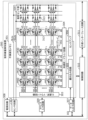
- FIG. 2 is a block diagram showing an example of the configuration of the radiation dose detection device 300 according to the embodiment.
- the radiation dose detection device 300 according to the present embodiment is composed of a semiconductor integrated circuit, and includes a nonvolatile memory 301 on a semiconductor substrate.
- This nonvolatile memory 301 includes a memory array 302 composed of memory cells M00 to Mxy arranged two-dimensionally, a row selection/driver circuit 303, a column selection/driver circuit 304, and a memory array 302 for writing information.
- the amount of current flowing through the write circuit 305 and the selected memory cells M00 to Mxy through the selected bit line is detected, and the information stored in the selected memory cells M00 to Mxy is determined as data "1" or " 0'', and a data input/output circuit 307 that performs input/output processing of input/output data via a signal node DQ.
- the radiation dose detection device 300 also has a power supply circuit 308 that generates various power supplies used inside the memory from an external power supply, an address input circuit 309 that outputs address signals to the nonvolatile memory 301, and the outside of the device. It includes an external interface circuit 311 that transmits and receives address signals, data, and control signals, and a control circuit 310 that controls the entire radiation dose detection device 300 based on signals input and output via the external interface circuit 311.
- the control circuit 310 includes, for example, a memory that stores a control program, a processor that executes the control program, and the like.
- the radiation dose detection device 300 is created using a part of the memory array 302, and includes a temperature sensor unit 320 that senses the ambient temperature, and outputs data correlated with the temperature using the temperature sensor unit 320.
- a sensor circuit 312 is provided.
- the temperature sensor section 320 has the structure and circuit configuration shown in FIGS. 1(c) and 1(d).
- the sensor circuit 312 also has a radiation dose detection function, which will be described later.
- the memory array 302 includes a plurality of word lines WL0, WL1,...WLy formed on a semiconductor substrate, bit lines BL0, BL1,...BLx arranged to cross a plurality of word lines WL0, WL1,...WLy arranged parallel to each other, and a source.
- a plurality of transistors T00, T01, ..., Txy (hereinafter referred to as “transistors T00, T01, ") provided corresponding to the intersections with the lines SL0, SL1, ...SLx, respectively, and a transistor T00. , T01,... and variable resistance elements 313 provided one-to-one are connected in series (hereinafter referred to as "memory cells M00, M01,!). ”).
- Each of the memory cells M00 to Mxy has the structure shown in FIG. 1(a), and the circuit diagram markings thereof are in accordance with FIG. 1(b).
- the variable resistance element 313 operates as a nonvolatile memory element within the memory cells M00 to Mxy.
- Each of such memory cells M00 to Mxy is composed of one selection transistor 319 and one resistance change element 313, and is therefore called a 1T1R type memory cell.
- the column selection/driver circuit 304 selects one bit line (BL) and one source line (SL), and the row selection/driver circuit 303 selects one word line, the selected bit line and source line , one memory cell intersected by the word line is selected. That is, one memory cell is selected from memory array 302. Note that although the configuration of the nonvolatile memory 301 shown in FIG. 2 is such that one memory cell is selected, it is easy to change the configuration so that multiple memory cells can be accessed simultaneously by arranging circuits in parallel. This is a design matter.
- FIG. 3 is a graph showing an example of the resistance value range of the resistance change elements 313 included in the memory cells M00 to Mxy shown in FIG. 2.
- the variable resistance elements 313 included in the memory cells M00 to Mxy have at least two states: a variable state and an initial state.
- the variable state refers to a state in which the resistance value can reversibly transition between variable resistance ranges by applying different electrical signals.
- the initial state refers to a state in which no electrical stress is applied to the variable resistance element 313 after the completion of the semiconductor manufacturing process, and an initial state where the resistance value is high and does not overlap with any of the variable resistance ranges. A state in which the resistance value is within the range.
- variable resistance element 313 in the initial state does not become variable unless forming stress, which is an electrical stress that changes it to the variable state, is applied.
- forming stress may be cumulative electrical stress. In that case, when the cumulative amount of stress exceeds a predetermined amount, the initial state transitions to the variable state.
- the memory array 302 in FIG. 2 can be made variable by individually selecting all the memory cells M00 to Mxy and applying forming stress to the variable resistance element 313 included in the selected memory cell. state, store desired data, and read the stored data as needed.
- the resistance change element 313 included in the temperature sensor section 320 is maintained in its initial state.
- the resistance change element 313 included in the temperature sensor section 320 has the configuration shown in FIGS. 1(c) and 1(d). That is, the drain of the selection transistor 319 has no plug layer 317, is not connected to the variable resistance element 313, and is grounded (grounding is not shown). The source of the selection transistor 319 is not connected to the source line but is grounded (grounding is not shown). All the plurality of variable resistance elements 313 included in the temperature sensor section 320 are connected in parallel between the temperature sensor source line SLts and the temperature sensor bit line BLts.
- FIG. 4 is a graph showing an example of the temperature characteristics of the resistance change element 313 in an initial state that constitutes the temperature sensor section 320 included in the radiation dose detection device 300 according to the embodiment. Good resistance changes are shown with respect to temperature changes.
- the plurality of resistance change elements 313 in the initial state are connected in parallel between the temperature sensor bit line BLts and the temperature sensor source line SLts.
- the resistance value between the source line SLts and the source line SLts is the combined resistance of the plurality of variable resistance elements 313 in the initial state.
- FIG. 5 is a block diagram showing the circuit configuration of the sensor circuit 312 in FIG. 2.
- the detailed circuit configuration of the power supply circuit 308 and the temperature sensor section 320 are also shown in order to show the relationship with peripheral circuits.
- a power supply circuit 308 shown in FIG. 5 includes a bandgap reference circuit BGR that generates an adjustable reference voltage Vref, and a regulator circuit 308a that outputs a power supply voltage Vreg in accordance with the reference voltage Vref.
- Regulator circuit 308a includes an operational amplifier 308b, a transistor 308c, and resistance elements R1 and R2.
- the operational amplifier 308b compares the reference voltage Vref output by the bandgap reference circuit BGR with the voltage divided by the resistors R1 and R2, and adjusts the voltage level at the gate of the transistor 308c so that these voltages become equal. adjust.
- the input voltage Vin input to the transistor 308c is a voltage higher than the output power supply voltage Vreg by more than the drop voltage caused by the transistor 308c.
- the reference voltage Vref output by the bandgap reference circuit BGR is calibrated by the adjustment voltage Vtrim input from the control circuit 310.
- the calibration value of the adjustment voltage Vtrim is determined by inspection before shipping, and is stored in the memory array 302. Therefore, the control circuit 310 reads the calibration value stored in the memory array 302 and outputs it to the bandgap reference circuit BGR as the adjustment voltage Vtrim, so that the reference voltage Vref and power supply voltage Vreg are always calibrated within a predetermined range. is output.
- the bandgap reference circuit BGR is a well-known technology, and detailed circuit configuration and explanation will be omitted. Note that in a wireless communication device such as an RF tag, a DC voltage obtained by rectifying an AC voltage generated in a communication antenna by a rectifier circuit is input to the power supply circuit 308 as an input voltage Vin.
- the temperature sensor section 320 is a temperature sensor that functions as a first current source that outputs a first current that depends on the ambient temperature of the radiation dose detection device 300 using the power supply voltage Vreg, and is shown in (c) of FIG.
- the power supply voltage Vreg is applied to the first node 320a, and the second node 320b outputs the first current.
- the temperature sensor section 320 is configured by connecting a plurality of variable resistance elements 313 in parallel, and the combined resistance is obtained by averaging the variations in resistance value of each of the plurality of variable resistance elements 313. value.
- the temperature sensor section 320 may be configured with one resistance change element 313.
- the sensor circuit 312 includes a radiation sensor unit 340 that functions as a second current source that outputs a second current that depends on the radiation dose with which the radiation dose detection device 300 is irradiated, and a radiation sensor unit 340 that uses the power supply voltage Vreg to output a second current that depends on the radiation dose irradiated with the radiation dose detection device 300. and a detection circuit 350 that outputs a first signal indicating the temperature corresponding to the magnitude of the current and a second signal indicating the radiation dose corresponding to the magnitude of the second current.
- the radiation sensor section 340 includes a transistor TRsp such as a p-type MOS transistor whose threshold voltage VT changes depending on the irradiated radiation dose, a resistance element R4 connected between the source and gate of the transistor TRsp, and a transistor TRsp.
- the resistor element R3 is connected between the gate of the resistor R3 and the ground.
- the power supply voltage Vreg is applied to one terminal (source terminal) of the transistor TRsp, and the other terminal (drain terminal) of the transistor TRsp outputs a second current.
- the detection circuit 350 includes a selection circuit 345 having two switch elements 343 and 344 that are exclusively short-circuited in order to select one of the first current and the second current and output it as a third current as a power supply current Iro.
- the ring oscillator 341 receives the power supply current Iro output from the selection circuit 345 and outputs a clock with a frequency corresponding to the power supply current Iro, and the clock output from the ring oscillator 341 is counted for a predetermined period of time.
- the counter circuit 342 outputs the counted value as a first signal or a second signal.
- the oscillation frequency of the ring oscillator 341 changes depending on the amount of power supply current Iro supplied to the ring oscillator 341.
- the output of the ring oscillator 341 is input to the counter circuit 342 as an operating clock, and when the Reset signal input from the control circuit 310 is H, the count value is reset to zero, and the Enable signal input from the control circuit 310 is H.
- the number of clocks is counted according to the input clock.
- the period during which the Enable signal is high has a certain pulse width, and is designed so that the oscillation frequency of the ring oscillator 341 can be determined from the count value Dat output from the counter circuit 342.
- the count value Dat output by the counter circuit 342 is input to the control circuit 310 and output to the outside of the radiation dose detection device 300.
- the power supply current Iro is supplied from the power supply voltage Vreg via the combined resistance of the plurality of variable resistance elements 313 forming the temperature sensor section 320. Since the combined resistance of the temperature sensor section 320 has good temperature characteristics as shown in FIG. 4, it is possible to obtain a count value Dat corresponding to the ambient temperature.
- the drain-source current determined by the gate voltage Vpg and threshold voltage VT of the transistor TRsp becomes the power supply current Iro
- the power supply current Iro becomes the ring oscillator 341 supplied to
- the oscillation frequency of the ring oscillator 341 changes. This change in oscillation frequency is obtained as a change in the count value Dat obtained from the counter circuit 342, and the degree of exposure to radiation can be quantitatively obtained. Note that the change in the threshold voltage VT of the transistor TRsp due to exposure to radiation is maintained even after the exposure to radiation ends.
- FIG. 6 is a diagram showing an example of a measurement result obtained by measuring the ambient temperature using the temperature sensor section 320 and the sensor circuit 312 included in the radiation dose detection device 300 according to the embodiment.
- the graph in FIG. 6A shows temperature characteristics in which the horizontal axis is temperature and the vertical axis is a value obtained by converting the count value Dat obtained from the counter circuit 342 into frequency.
- (a) in FIG. 6 shows the initial temperature characteristics before exposing the radiation dose detection device 300 to radiation (dotted line of “0 KGy”) and the temperature characteristics after exposing the radiation dose detection device 300 to a radiation dose of 25 KGy.
- the measured temperature characteristics (solid line of "25 KGy”) are shown.
- the graph in FIG. 6(b) shows radiation dose-dependent characteristics with the horizontal axis representing the amount of radiation exposure and the vertical axis representing the frequency. As can be seen from FIG. 6(b), it is shown that the frequency of each temperature is almost constant. Note that the graphs shown in FIGS. 6(a) and 6(b) show measurement results obtained by adjusting the reference voltage Vref so that the power supply voltage Vreg becomes equal before and after radiation irradiation. ing.
- the parallel combined resistance of the temperature sensor section 320 exhibits favorable changes depending on temperature, and its temperature characteristics are hardly affected by radiation exposure.
- the radiation dose detection device 300 according to the present embodiment utilizes this fact, and can function as a good radiation-resistant temperature sensor without degrading detection accuracy against radiation exposure.
- the semiconductor integrated circuit that constitutes the radiation dose detection device 300 is an assembly of circuits made up of transistors, the threshold voltage VT changes due to exposure to radiation, causing fluctuations in circuit operation.
- the reference voltage Vref output by the bandgap reference circuit BGR is important because it serves as a reference for all built-in analog circuits.
- the radiation dose detection device 300 uses the temperature sensor section 320 whose temperature characteristics hardly change due to radiation exposure, so that the radiation dose of the radiation dose detection device 300 due to radiation exposure is reduced. Equipped with a calibration function that responds to changes in detection characteristics (returns to original characteristics). Calibration performed after radiation exposure will be described below.
- FIG. 7 is a flowchart showing the procedure of a radiation dose detection method including a calibration function by the radiation dose detection device 300 according to the embodiment.
- the adjustment voltage Vtrim is adjusted so that the power supply voltage Vreg shown in FIG. ing.
- the value of the adjusted voltage Vtrim adjusted at this time is set as a value Vtrim0, and the values of the obtained reference voltage Vref and power supply voltage Vreg are set as a value Vref0 and a value Vreg0, respectively.
- temperature characteristics are measured using the temperature sensor section 320 and the sensor circuit 312 under the power supply voltage Vreg of value Vreg0, and the measurement results are stored in the memory array 302 of the nonvolatile memory 301 (S10). More specifically, the control circuit 310 stores in the memory array 302, for example, a count value C25 obtained from the counter circuit 342 of the sensor circuit 312 at a room temperature of 25 degrees and a count value C85 at a temperature of 85 degrees. If the relationship between the temperature at two points and the count value is known, a characteristic function of temperature characteristics as shown in FIG. 4 can be derived, and the ambient temperature can be monitored from the obtained count value.
- the selection circuit 345 selects the first current, and the first correlation between the ambient temperature and the count value output by the counter circuit 342 is calculated before the radiation irradiation. This corresponds to a first acquisition step of acquiring (that is, the temperature characteristics of the temperature sensor section 320).
- control circuit 310 also acquires the already stored temperature characteristics of the radiation sensor section 340 from the memory array 302 of the nonvolatile memory 301 (S11). For example, a function indicating how the measured radiation dose should be corrected depending on the ambient temperature, that is, a function indicating the temperature dependence of the measured radiation dose is obtained.
- This step S11 corresponds to a third acquisition step of acquiring a third correlation indicating the temperature dependence of the count value output by the counter circuit 342 while the selection circuit 345 selects the second current.
- the radiation dose detection device 300 is exposed to radiation for sterilization and the like (S12). After exposure to radiation, the power supply voltage Vreg adjusted by the trimming value Vtrim0 changes due to the influence of the radiation and is no longer the voltage Vreg0.
- step S10 the radiation dose detection device 300 to be calibrated stores the count value C25 and the count value C85 in the memory array 302 before shipping, so the control circuit 310 stores the count value C25 and the count value C85.
- the control circuit 310 By reading out and count value C85 from the memory array 302, a function indicating temperature characteristics is obtained.
- An expected count value Ct corresponding to the current temperature Tc is calculated from the obtained temperature characteristic function.
- step S13 after radiation irradiation, the control circuit 310 obtains a second correlation between the ambient temperature and the count value output by the counter circuit 342 while the selection circuit 345 selects the first current.
- step S14 corresponds to an adjustment step in which the control circuit 310 adjusts the reference voltage so that the first correlation and the second correlation are equal.
- the value Vreg1 will be equal to the value Vreg0 before radiation exposure.
- the calibrated Vtrim value is stored in memory array 302, thereby updating the trim value.
- the control circuit 310 short-circuits only the switch element 344 in the selection circuit 345, operates the radiation sensor section 340, and obtains a count value, thereby calculating the radiation dose (S15).
- This step S15 corresponds to a radiation dose detection step in which the selection circuit 345 selects the second current under the control of the control circuit 310 and detects the radiation dose.
- control circuit 310 uses the temperature characteristics of the radiation sensor unit 340 acquired in step S11 to calculate the radiation dose after temperature correction from the current temperature Tc and the radiation dose obtained in step S15. (S16).
- the temperature characteristics of the temperature sensor section 320 can be adjusted by calibrating the power supply voltage Vreg after radiation exposure to the same voltage as before exposure. are the same before and after radiation irradiation as shown in FIG. Provided as a temperature sensor.
- the above-mentioned power supply voltage is calibrated after exposure to radiation, and the ring oscillator 341 is operated by the power supply current Iro supplied by the radiation sensor section 340 while the power supply voltage Vreg is kept constant, and the counter By obtaining the count value in the circuit 342, it is possible to accurately monitor the amount of radiation exposure that is not affected by radiation exposure.
- step S11 may be performed at any stage before step S16. Further, in step S10, if the obtained first correlation is stored in the memory array 302, the first correlation may be acquired at any stage before step S14. .
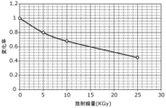
- FIG. 8 shows an example of the relationship between the radiation dose irradiated to the radiation dose detection device 300 according to the embodiment (horizontal axis) and the frequency change rate (vertical axis) based on the obtained count value. It is a diagram. Here, the results are obtained by implementing the calibration method shown in FIG. 7. Note that the rate of change on the vertical axis is the rate of change in the measured frequency when the initial frequency before exposure to radiation is set to 1. Because each radiation dose detection device is affected by individual variations due to circuit process variations, etc., the frequency varies, so by using the rate of change instead of frequency, the radiation dose can be measured without depending on the radiation dose detection device. can be monitored. As can be seen from FIG.
- the frequency decreases with a negative correlation with the irradiated radiation dose. Utilizing this characteristic, the count value output from the counter circuit 342 reveals an accurate amount of radiation exposure that is hardly affected by radiation exposure.
- the radiation dose detection device 300 uses the power supply circuit 308 that outputs the power supply voltage Vreg and the first current that depends on the ambient temperature of the radiation dose detection device 300 using the power supply voltage Vreg.
- the radiation dose detection device 300 functions as a second current source that outputs a second current depending on the irradiated radiation dose using the temperature sensor section 320 that functions as a first current source that outputs the radiation dose and the power supply voltage Vreg. It includes a radiation sensor section 340 and a detection circuit 350 that outputs a first signal indicating the temperature corresponding to the magnitude of the first current and a second signal indicating the radiation dose corresponding to the magnitude of the second current.
- the temperature sensor section 320 includes a first electrode layer 316, a second electrode layer 314, and a variable resistance layer 315 containing a transition metal oxide interposed between the first electrode layer 316 and the second electrode layer 314.
- a second node 320b is connected to each other, the power supply voltage Vreg is applied to the first node 320a, the second node 320b outputs the first current, and the second current source is connected to the transistor TRsp.
- a power supply voltage Vreg is applied to one terminal of the transistor TRsp, and the other terminal of the transistor TRsp outputs a second current.
- the radiation dose detection device 300 not only enables the temperature sensor section 320 to detect temperature, but also allows the temperature sensor section 320 to be a resistor containing a transition metal oxide that is hardly affected by radiation exposure. By utilizing the characteristic of being composed of variable elements, it becomes possible to respond to changes in the characteristics of the radiation dose detection device due to radiation exposure.
- the transition metal oxide is, for example, at least one of aluminum oxide, tantalum oxide, hafnium oxide, and zirconium oxide.
- the radiation dose detection device 300 includes a resistance change type nonvolatile memory 301 in which a plurality of resistance change elements 313 are arranged in an array, and one or more resistance change elements 313 included in the temperature sensor section 320 are nonvolatile memory This is a part of a plurality of resistance change elements 313 that constitute 301.
- one or more resistance change elements 313 included in the temperature sensor section 320 are configured as a part of the plurality of resistance change elements 313 that constitute the nonvolatile memory 301, so that the temperature sensor section 320 can be and nonvolatile memory 301 can be manufactured.
- dummy cells that are not used for data storage are generally arranged at the outer periphery of the array in order to ensure processing uniformity in the manufacturing process. Therefore, by using the dummy cell in the temperature sensor section 320, there is no need to add a separate cell for this device, and the circuit area can be used effectively.
- the detection circuit 350 also receives a selection circuit 345 that selects one of the first current and the second current and outputs it as a third current, and a third current output from the selection circuit 345, and outputs the third current as the third current.
- a ring oscillator 341 that outputs a clock of a corresponding frequency
- a counter circuit 342 that counts the clock output from the ring oscillator 341 for a predetermined period of time and outputs the obtained count value as a first signal or a second signal. have This allows the common detection circuit 350 to measure the first current and the second current, thereby reducing the circuit scale.
- the power supply circuit 308 includes a bandgap reference circuit BGR that generates an adjustable reference voltage Vref, and a regulator circuit 308a that outputs a power supply voltage Vreg in accordance with the reference voltage Vref.
- a bandgap reference circuit BGR that generates an adjustable reference voltage Vref
- a regulator circuit 308a that outputs a power supply voltage Vreg in accordance with the reference voltage Vref.
- the radiation dose detection device 300 further calculates the first count value output by the counter circuit 342 before radiation irradiation, the first ambient temperature when the first count value is output, and the counter circuit 342 after radiation irradiation. From the second count value output by the circuit 342 and the second ambient temperature at the time the second count value is output, a first correlation between the first count value and the first ambient temperature and a second count value are determined.
- a control circuit 310 is provided that adjusts the reference voltage Vref so that the second correlation with the second ambient temperature is equal. Thereby, by adjusting the reference voltage Vref so as to match the temperature characteristics of the temperature sensor section 320 before and after radiation exposure, the same power supply voltage Vreg can be maintained before and after radiation exposure.
- the radiation dose detection method is a radiation dose detection method using the radiation dose detection device 300, in which the selection circuit 345 selects the first current and the ambient temperature is adjusted before radiation irradiation.
- the radiation dose detection method further includes a third acquisition step of acquiring a third correlation indicating the temperature dependence of the count value output by the counter circuit 342 while the selection circuit 345 selects the second current;
- the third correlation is used to calculate the temperature-corrected radiation dose from the count value output by the counter circuit 342 obtained by detecting the radiation dose.
- the temperature dependence of the radiation sensor section 340 is corrected, and a radiation dose after temperature correction is obtained.
- the present disclosure is not limited to the embodiments.
- the scope of the present disclosure also includes various modifications that can be thought of by those skilled in the art to the present embodiment, and other forms constructed by combining some of the constituent elements of the embodiments, as long as they do not depart from the spirit of the present disclosure. contained within.
- the detection circuit 350 includes the ring oscillator 341, but it does not necessarily need to include such a configuration.
- the detection circuit 350 may be a circuit configured with a current-voltage converter and an A/D converter, etc., as long as it outputs a digital value that depends on the power supply current Iro output from the temperature sensor section 320 or the radiation sensor section 340. It may also be configured with other circuits.
- the power supply circuit 308 has a function of adjusting the power supply voltage Vreg, but a circuit for adjusting the power supply voltage Vreg output from the power supply circuit 308 may be provided outside the power supply circuit 308. .
- the radiation dose detection device is used as a sensor that maintains good temperature and radiation dose sensing accuracy even after exposure to radiation, and is used as a sensor that is configured of, for example, a semiconductor integrated circuit device and whose life cycle is managed; Alternatively, it is subjected to radiation sterilization while still attached to the packaging material containing it, and by calibrating the circuit operating voltage using RF communication, it is possible to manage the life cycle of the object without deteriorating sensing accuracy. It can be used as an RFID tag. That is, since it can be used as an RFID that excludes the influence of radiation, it is possible to save the effort of attaching and detaching an RFID tag attached to an object whose life cycle is to be managed before and after radiation irradiation.
- Nonvolatile memory 302 Memory array 303 Row selection/driver circuit 304 Column selection/driver circuit 305 Write circuit 306 Sense amplifier 307 Data input/output circuit 308 Power supply circuit 308a Regulator circuit 308b Operational amplifier 308c Transistor 309 Address input circuit 310 Control circuit 311 External interface circuit 312 Sensor circuit 313 Resistance change element 314 Second electrode layer 315 Variable resistance layer 315a Second tantalum oxide layer 315b First tantalum oxide layer 316 First electrode layer 317 Plug layer 318 Metal wiring Layer 319 Selection transistor 320 Temperature sensor section 320a First node 320b Second node 340 Radiation sensor section 341 Ring oscillator 342 Counter circuit 343, 344 Switch element 345 Selection circuit 350 Detection circuit BGR Band gap reference circuit BL0 to BLx Bit line BLts Temperature sensor Bit line for M00 ⁇ Mxy Memory cell SL0 ⁇ SLx Source line SLts Source line for temperature sensor T00 ⁇ Txy, TRsp
Abstract
Dispositif de détection de quantité de rayonnement (300) comprenant : un circuit d'alimentation électrique (308) qui délivre une tension d'alimentation électrique (Vreg); un ensemble capteur de température (320) qui fonctionne en tant que première source de courant pour délivrer un premier courant en fonction de la température ambiante à l'aide de la tension d'alimentation électrique (Vreg) ; un ensemble capteur de rayonnement (340) qui fonctionne en tant que seconde source de courant pour délivrer, à l'aide de la tension d'alimentation électrique (Vreg), un second courant en fonction de la quantité de rayonnement à laquelle le dispositif de détection de quantité de rayonnement (300) a été exposé ; et un circuit de détection (350) qui délivre un premier signal indiquant une température correspondant à l'intensité du premier courant, et qui délivre un second signal indiquant une quantité de rayonnement correspondant à l'intensité du second courant. L'ensemble capteur de température (320) comprend un ou plusieurs éléments de variation de la résistance (313) qui comprennent une couche à résistance variable (315) contenant un oxyde de métal de transition. La seconde source de courant comprend un transistor (TRsp).
Applications Claiming Priority (2)
| Application Number | Priority Date | Filing Date | Title |
|---|---|---|---|
| JP2022-053592 | 2022-03-29 | ||
| JP2022053592 | 2022-03-29 |
Publications (1)
| Publication Number | Publication Date |
|---|---|
| WO2023190086A1 true WO2023190086A1 (fr) | 2023-10-05 |
Family
ID=88202147
Family Applications (1)
| Application Number | Title | Priority Date | Filing Date |
|---|---|---|---|
| PCT/JP2023/011651 WO2023190086A1 (fr) | 2022-03-29 | 2023-03-23 | Dispositif de détection de quantité de rayonnement et procédé de détection de quantité de rayonnement |
Country Status (1)
| Country | Link |
|---|---|
| WO (1) | WO2023190086A1 (fr) |
Citations (7)
| Publication number | Priority date | Publication date | Assignee | Title |
|---|---|---|---|---|
| JPH10512416A (ja) * | 1995-03-20 | 1998-11-24 | サラド ゲゼルシャフト フア コンプレックス ライスツンゲン ツア ザニールンク ラジオローギッシュ ベラステーテル オブジェクテ エム・ベー・ハー | 放射線の入射頻度を検出するための放射線センサ手段 |
| JP2002277556A (ja) * | 2001-02-22 | 2002-09-25 | Koninkl Philips Electronics Nv | コンピュータ断層撮影装置用の放射線センサ及び放射線検出器 |
| JP2013088380A (ja) * | 2011-10-21 | 2013-05-13 | Furukawa Co Ltd | 携帯型放射線検出器 |
| JP2015190819A (ja) * | 2014-03-28 | 2015-11-02 | 三菱電機株式会社 | 放射性ガスモニタ |
| JP2016015192A (ja) * | 2014-06-12 | 2016-01-28 | パナソニックIpマネジメント株式会社 | データ記録方法および不揮発性記憶装置 |
| JP2016031274A (ja) * | 2014-07-29 | 2016-03-07 | 日本電気株式会社 | 抵抗変化素子を用いたデジタル温度センサ及びコントローラ |
| US20210097363A1 (en) * | 2019-09-26 | 2021-04-01 | Best Medical Canada Ltd. | Low power non-volatile non-charge-based variable supply rfid tag memory |
-
2023
- 2023-03-23 WO PCT/JP2023/011651 patent/WO2023190086A1/fr unknown
Patent Citations (7)
| Publication number | Priority date | Publication date | Assignee | Title |
|---|---|---|---|---|
| JPH10512416A (ja) * | 1995-03-20 | 1998-11-24 | サラド ゲゼルシャフト フア コンプレックス ライスツンゲン ツア ザニールンク ラジオローギッシュ ベラステーテル オブジェクテ エム・ベー・ハー | 放射線の入射頻度を検出するための放射線センサ手段 |
| JP2002277556A (ja) * | 2001-02-22 | 2002-09-25 | Koninkl Philips Electronics Nv | コンピュータ断層撮影装置用の放射線センサ及び放射線検出器 |
| JP2013088380A (ja) * | 2011-10-21 | 2013-05-13 | Furukawa Co Ltd | 携帯型放射線検出器 |
| JP2015190819A (ja) * | 2014-03-28 | 2015-11-02 | 三菱電機株式会社 | 放射性ガスモニタ |
| JP2016015192A (ja) * | 2014-06-12 | 2016-01-28 | パナソニックIpマネジメント株式会社 | データ記録方法および不揮発性記憶装置 |
| JP2016031274A (ja) * | 2014-07-29 | 2016-03-07 | 日本電気株式会社 | 抵抗変化素子を用いたデジタル温度センサ及びコントローラ |
| US20210097363A1 (en) * | 2019-09-26 | 2021-04-01 | Best Medical Canada Ltd. | Low power non-volatile non-charge-based variable supply rfid tag memory |
Similar Documents
| Publication | Publication Date | Title |
|---|---|---|
| US7896545B2 (en) | Apparatus and methods for temperature calibration and sensing | |
| JP6067792B2 (ja) | 半導体プロセスセンサおよび半導体プロセスを特徴付ける方法 | |
| US7656734B2 (en) | Methods and apparatus for extending the effective thermal operating range of a memory | |
| US7383149B1 (en) | Semiconductor device having variable parameter selection based on temperature and test method | |
| US7417448B2 (en) | System to calibrate on-die temperature sensor | |
| US7773446B2 (en) | Methods and apparatus for extending the effective thermal operating range of a memory | |
| JP5479657B1 (ja) | 不揮発性記憶装置、およびそのフォーミング方法 | |
| US7502710B2 (en) | Temperature detection circuit | |
| US20110141824A1 (en) | Leakage compensated reference voltage generation system | |
| US20080106322A1 (en) | On die thermal sensor in semiconductor memory device | |
| US20020173930A1 (en) | Method and device for determining an operating temperature of a semiconductor component | |
| WO2023190086A1 (fr) | Dispositif de détection de quantité de rayonnement et procédé de détection de quantité de rayonnement | |
| KR20230169011A (ko) | 기입 펄스 트리밍을 갖는 메모리 디바이스 | |
| US7139186B2 (en) | Failure detection circuit | |
| US20130160518A1 (en) | Relative humidity sensor and method for calibration thereof | |
| US11081177B2 (en) | Generating a reference current for sensing | |
| US11619961B1 (en) | Bandgap reference compensation circuit | |
| US11378603B2 (en) | Voltage or current detector for a memory component | |
| JP2005116634A (ja) | 複数の基準電圧発生回路を含む半導体装置及びその製造方法 | |
| US11636896B2 (en) | Memory cell array circuit and method of forming the same |
Legal Events
| Date | Code | Title | Description |
|---|---|---|---|
| 121 | Ep: the epo has been informed by wipo that ep was designated in this application |
Ref document number: 23780096 Country of ref document: EP Kind code of ref document: A1 |