EP0803943A2 - Oberflächenemittierende Diodenlasereinheit mit optischer Leistungsüberwachung - Google Patents
Oberflächenemittierende Diodenlasereinheit mit optischer Leistungsüberwachung Download PDFInfo
- Publication number
- EP0803943A2 EP0803943A2 EP97302521A EP97302521A EP0803943A2 EP 0803943 A2 EP0803943 A2 EP 0803943A2 EP 97302521 A EP97302521 A EP 97302521A EP 97302521 A EP97302521 A EP 97302521A EP 0803943 A2 EP0803943 A2 EP 0803943A2
- Authority
- EP
- European Patent Office
- Prior art keywords
- surface laser
- laser diode
- optical power
- monitor
- lower mirror
- Prior art date
- Legal status (The legal status is an assumption and is not a legal conclusion. Google has not performed a legal analysis and makes no representation as to the accuracy of the status listed.)
- Granted
Links
Images
Classifications
-
- H—ELECTRICITY
- H01—ELECTRIC ELEMENTS
- H01S—DEVICES USING THE PROCESS OF LIGHT AMPLIFICATION BY STIMULATED EMISSION OF RADIATION [LASER] TO AMPLIFY OR GENERATE LIGHT; DEVICES USING STIMULATED EMISSION OF ELECTROMAGNETIC RADIATION IN WAVE RANGES OTHER THAN OPTICAL
- H01S3/00—Lasers, i.e. devices using stimulated emission of electromagnetic radiation in the infrared, visible or ultraviolet wave range
- H01S3/09—Processes or apparatus for excitation, e.g. pumping
- H01S3/091—Processes or apparatus for excitation, e.g. pumping using optical pumping
- H01S3/094—Processes or apparatus for excitation, e.g. pumping using optical pumping by coherent light
- H01S3/0941—Processes or apparatus for excitation, e.g. pumping using optical pumping by coherent light of a laser diode
-
- H—ELECTRICITY
- H01—ELECTRIC ELEMENTS
- H01S—DEVICES USING THE PROCESS OF LIGHT AMPLIFICATION BY STIMULATED EMISSION OF RADIATION [LASER] TO AMPLIFY OR GENERATE LIGHT; DEVICES USING STIMULATED EMISSION OF ELECTROMAGNETIC RADIATION IN WAVE RANGES OTHER THAN OPTICAL
- H01S5/00—Semiconductor lasers
- H01S5/02—Structural details or components not essential to laser action
- H01S5/026—Monolithically integrated components, e.g. waveguides, monitoring photo-detectors, drivers
- H01S5/0262—Photo-diodes, e.g. transceiver devices, bidirectional devices
- H01S5/0264—Photo-diodes, e.g. transceiver devices, bidirectional devices for monitoring the laser-output
-
- H—ELECTRICITY
- H01—ELECTRIC ELEMENTS
- H01S—DEVICES USING THE PROCESS OF LIGHT AMPLIFICATION BY STIMULATED EMISSION OF RADIATION [LASER] TO AMPLIFY OR GENERATE LIGHT; DEVICES USING STIMULATED EMISSION OF ELECTROMAGNETIC RADIATION IN WAVE RANGES OTHER THAN OPTICAL
- H01S5/00—Semiconductor lasers
- H01S5/10—Construction or shape of the optical resonator, e.g. extended or external cavity, coupled cavities, bent-guide, varying width, thickness or composition of the active region
- H01S5/18—Surface-emitting [SE] lasers, e.g. having both horizontal and vertical cavities
- H01S5/183—Surface-emitting [SE] lasers, e.g. having both horizontal and vertical cavities having only vertical cavities, e.g. vertical cavity surface-emitting lasers [VCSEL]
- H01S5/18308—Surface-emitting [SE] lasers, e.g. having both horizontal and vertical cavities having only vertical cavities, e.g. vertical cavity surface-emitting lasers [VCSEL] having a special structure for lateral current or light confinement
- H01S5/18311—Surface-emitting [SE] lasers, e.g. having both horizontal and vertical cavities having only vertical cavities, e.g. vertical cavity surface-emitting lasers [VCSEL] having a special structure for lateral current or light confinement using selective oxidation
-
- H—ELECTRICITY
- H01—ELECTRIC ELEMENTS
- H01S—DEVICES USING THE PROCESS OF LIGHT AMPLIFICATION BY STIMULATED EMISSION OF RADIATION [LASER] TO AMPLIFY OR GENERATE LIGHT; DEVICES USING STIMULATED EMISSION OF ELECTROMAGNETIC RADIATION IN WAVE RANGES OTHER THAN OPTICAL
- H01S5/00—Semiconductor lasers
- H01S5/10—Construction or shape of the optical resonator, e.g. extended or external cavity, coupled cavities, bent-guide, varying width, thickness or composition of the active region
- H01S5/1078—Construction or shape of the optical resonator, e.g. extended or external cavity, coupled cavities, bent-guide, varying width, thickness or composition of the active region with means to control the spontaneous emission, e.g. reducing or reinjection
Definitions
- the present invention relates to a surface laser diode package having a monitor diode for monitoring an optical power of a surface laser diode.
- a general optical disc system such as a compact disc player projects laser light on an information recording surface of a disc and reads information recorded on the disc.
- the optical disc system includes an automatic laser power control (ALPC) servo circuit to stably control the output of the laser light.
- the ALPC servo circuit includes a photodiode for monitoring an optical power of a laser diode, and keeps a driving current of the laser diode constant according to the current flowing through the photodiode.
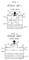
- Conventional surface laser diode packages will be described below with reference to Figures 1 and 2.
- a monitor diode 15 has a cylindrical shape wrapping around a surface laser diode 12.
- the monitor diode 15 detects a spontaneous emission beam emitted from the lateral surface of the surface laser diode 12.
- the detected beam is used to monitor an optical power of the surface laser diode 12. If a current is applied to an electrode 11 of the surface laser diode 12, the current is supplied to an active region 13. If the current is supplied to the active region 13, the surface laser diode 12 generates a spontaneous emission beam. If the current supplied to the active region 13 is not less than a current value necessary for laser oscillation, the spontaneous emission beam generated from the active region 13 is transformed into a surface laser beam by the laser oscillation.
- the beam emitted from the active region 13 oscillates in an upper mirror 121 and a lower mirror 123, and is emitted outwards via the upper mirror 121 and absorbed into a substrate 14 via the lower mirror 123.
- the upper mirror 121 and the lower mirror 123 interposing the active region 13 are used as a resonator.
- a current density should be large to generate a surface laser beam.
- portions outside a laser oscillation area between the upper mirror 121 and the lower mirror 123 are processed by oxidation or proton implantation to form a high ohmic layer to thereby enlarge a current density.
- the spontaneous emission beam generated by the active region 13 does not completely vanish and is minutely emitted in proportion to the optical power of the surface laser diode 12.
- the monitor diode 15 receives the spontaneous emission beam emitted from the sides of the surface laser diode 12 when current is applied to an electrode 16 of the monitor diode 15, and outputs a monitor current in proportion to the received beam.
- the surface laser diode package of Figure 1 is poor in terms of temperature characteristic. Thus, if temperature varies, an accurate monitor current cannot be output. Also, a spontaneous emission beam is used instead of a surface laser beam, to thereby cause an error in the optical power monitoring.
- a surface laser diode package of Figure 2 has a structure where a monitor diode 15 is installed on a surface laser diode 12.
- the monitor diode 15 detects part of a surface laser beam emitted from the surface laser diode 12 when current is applied to an electrode 16 of the monitor diode 15.
- the detected beam is used for monitoring an optical power of the surface laser diode 12.
- the monitor diode 15 detects the spontaneous emission beam as well as the surface laser beam emitted from the surface laser diode 12, an error has occurred in the optical power monitoring.
- the surface laser beam emitted to the external is used, the optical power of the surface laser diode 12 is lost and the manufacturing process becomes complicated.
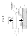
- a surface laser diode package capable of monitoring an optical power by detecting a surface laser beam except a spontaneous emission beam among beams emitted toward a substrate via a lower mirror of a surface laser diode.
- a surface laser diode package having an optical power monitoring function for a surface laser beam
- the surface laser diode package comprising: a substrate; a surface laser diode for making a spontaneous emission beam generated from an active region oscillate by means of an upper mirror and a lower mirror, and emitting a surface laser beam obtained by the oscillation; and a monitor diode, installed between the substrate and the lower mirror of the surface laser diode, for performing a light detection operation with respect to the surface laser beam emitted toward the substrate via the lower mirror, in order to monitor the optical power of the surface laser diode.
- the package comprises a light scattering portion, installed on a junction surface of said monitor diode and the lower mirror of said surface laser diode, for scattering the spontaneous emission beam incident via said lower mirror.
- said light scattering portion is installed on a region outside of a portion of said lower mirror corresponding to the surface from which the surface beam of said upper mirror is emitted.
- said light scattering portion is processed by oxidation.
- the present invention uses the fact that light emitted from an active region of a surface laser diode package is emitted in both the directions of an upper mirror and a lower mirror.
- a monitor diode 15 performs a light detection operation with respect to a laser beam emitted toward a substrate 14 via a lower mirror 123 of the surface laser diode 12.
- the monitor diode 15 is installed on a junction surface of a P-type substrate 14 and an N-type lower mirror 123 of the surface laser diode 12, and performs a light detection operation with respect to the beam emitted via the lower mirror 123.
- the monitor diode 15 generates a monitor current in proportion to the intensity of the incident laser beam.
- a reference numeral 16 represents the electrode of the monitor diode 15.
- Spontaneous emission beams generated by the active region 13 are randomly emitted in various directions, part of which oscillates by the upper mirror 121 and the lower mirror 123.
- the spontaneous emission beam which do not oscillate by the mirrors 121 and 123 causes incorrect monitoring of the optical power of the surface laser diode 12.
- a light scattering portion 30 is used to avoid the detection of the spontaneous emission beam.
- the light scattering portion 30 is formed by an oxidation process and is installed on the surface of the lower mirror 123 except a portion from which the surface laser beam is emitted.
- the spontaneous emission beam incident to the light scattering portion 30 is scattered therefrom. As a result, most of the spontaneous emission beam which do not oscillate is scattered by the light scattering portion 30 constituted by the oxidation processed layer.
- the surface laser beam generated by the surface laser diode 12 is incident to the monitor diode 15 via a portion where the light scattering portion 30 is absent. In this case, a little spontaneous emission beam is incident to the monitor diode 15 via the portion where the light scattering portion 30 is absent. However, since the incident spontaneous emission beam has very little intensity, the monitor current generated according to the optical power of the surface laser beam does not change. Thus, the monitor diode can output the monitor current which is proportional to the optical power of the surface laser diode 12.
- the surface laser diode package having an optical power monitoring function can monitor an optical power of the surface laser diode with more accuracy.
Landscapes
- Physics & Mathematics (AREA)
- Electromagnetism (AREA)
- Optics & Photonics (AREA)
- Condensed Matter Physics & Semiconductors (AREA)
- General Physics & Mathematics (AREA)
- Engineering & Computer Science (AREA)
- Plasma & Fusion (AREA)
- Semiconductor Lasers (AREA)
- Optical Head (AREA)
Applications Claiming Priority (2)
| Application Number | Priority Date | Filing Date | Title |
|---|---|---|---|
| KR1019960012985A KR0185950B1 (ko) | 1996-04-25 | 1996-04-25 | 레이저다이오드의 광출력모니터링패케지 |
| KR9612985 | 1996-04-25 |
Publications (3)
| Publication Number | Publication Date |
|---|---|
| EP0803943A2 true EP0803943A2 (de) | 1997-10-29 |
| EP0803943A3 EP0803943A3 (de) | 1998-04-29 |
| EP0803943B1 EP0803943B1 (de) | 2000-03-29 |
Family
ID=19456756
Family Applications (1)
| Application Number | Title | Priority Date | Filing Date |
|---|---|---|---|
| EP97302521A Expired - Lifetime EP0803943B1 (de) | 1996-04-25 | 1997-04-14 | Oberflächenemittierende Diodenlasereinheit mit optischer Leistungsüberwachung |
Country Status (6)
| Country | Link |
|---|---|
| US (1) | US6034981A (de) |
| EP (1) | EP0803943B1 (de) |
| JP (1) | JP2823849B2 (de) |
| KR (1) | KR0185950B1 (de) |
| CN (1) | CN1083600C (de) |
| DE (1) | DE69701544T2 (de) |
Cited By (3)
| Publication number | Priority date | Publication date | Assignee | Title |
|---|---|---|---|---|
| GB2346258A (en) * | 1999-01-30 | 2000-08-02 | Mitel Semiconductor Ab | Monitoring the light output of surface emitting lasers |
| DE10055884C2 (de) * | 1999-11-08 | 2002-10-24 | Korea Advanced Inst Sci & Tech | Oberflächenemissionslaser-Vorrichtung mit monolithisch integriertem Kontrollphotodetektor und Verfahren zu ihrer Herstellung |
| EP1513235A1 (de) * | 2003-08-07 | 2005-03-09 | Seiko Epson Corporation | VCSEL mit monolitisch integriertem Photodetektor und hybriden Spiegeln |
Families Citing this family (10)
| Publication number | Priority date | Publication date | Assignee | Title |
|---|---|---|---|---|
| US6368890B1 (en) * | 1999-05-05 | 2002-04-09 | Mitel Semiconductor Ab | Top contact VCSEL with monitor |
| KR20050019485A (ko) * | 2003-08-19 | 2005-03-03 | 삼성전자주식회사 | 광검출소자가 일체적으로 형성되는 수직 면발광 레이저 |
| US7418021B2 (en) * | 2004-06-25 | 2008-08-26 | Finisar Corporation | Optical apertures for reducing spontaneous emissions in photodiodes |
| US7746911B2 (en) * | 2004-06-25 | 2010-06-29 | Finisar Corporation | Geometric optimizations for reducing spontaneous emissions in photodiodes |
| US7310153B2 (en) * | 2004-08-23 | 2007-12-18 | Palo Alto Research Center, Incorporated | Using position-sensitive detectors for wavelength determination |
| JP4019285B2 (ja) * | 2005-02-04 | 2007-12-12 | セイコーエプソン株式会社 | 面発光型装置及びその製造方法 |
| US8437582B2 (en) | 2005-12-22 | 2013-05-07 | Palo Alto Research Center Incorporated | Transmitting light with lateral variation |
| US7718948B2 (en) * | 2006-12-04 | 2010-05-18 | Palo Alto Research Center Incorporated | Monitoring light pulses |
| JP2011096787A (ja) * | 2009-10-28 | 2011-05-12 | Sony Corp | 半導体発光装置 |
| TWI675522B (zh) * | 2019-01-15 | 2019-10-21 | 晶智達光電股份有限公司 | 發光元件 |
Family Cites Families (6)
| Publication number | Priority date | Publication date | Assignee | Title |
|---|---|---|---|---|
| JPS63118259U (de) * | 1987-01-24 | 1988-07-30 | ||
| JPS63118259A (ja) * | 1987-07-21 | 1988-05-23 | Canon Inc | インクカセット |
| JPH01146142A (ja) * | 1987-12-02 | 1989-06-08 | Mitsubishi Electric Corp | 2ビーム半導体レーザ装置 |
| JP3099921B2 (ja) * | 1992-09-11 | 2000-10-16 | 株式会社東芝 | 受光素子付き面発光型半導体レーザ装置 |
| US5475701A (en) * | 1993-12-29 | 1995-12-12 | Honeywell Inc. | Integrated laser power monitor |
| KR100259490B1 (ko) * | 1995-04-28 | 2000-06-15 | 윤종용 | 광검출기 일체형 표면광 레이저와 이를 채용한 광픽업 장치 |
-
1996
- 1996-04-25 KR KR1019960012985A patent/KR0185950B1/ko not_active Expired - Fee Related
-
1997
- 1997-04-14 EP EP97302521A patent/EP0803943B1/de not_active Expired - Lifetime
- 1997-04-14 DE DE69701544T patent/DE69701544T2/de not_active Expired - Fee Related
- 1997-04-18 CN CN97110583A patent/CN1083600C/zh not_active Expired - Fee Related
- 1997-04-23 JP JP9106183A patent/JP2823849B2/ja not_active Expired - Fee Related
- 1997-04-25 US US08/845,470 patent/US6034981A/en not_active Expired - Fee Related
Cited By (5)
| Publication number | Priority date | Publication date | Assignee | Title |
|---|---|---|---|---|
| GB2346258A (en) * | 1999-01-30 | 2000-08-02 | Mitel Semiconductor Ab | Monitoring the light output of surface emitting lasers |
| US6879611B1 (en) | 1999-01-30 | 2005-04-12 | Zarlink Semiconductor Ab | VCSEL with monitor emission through high reflectivity mirror |
| DE10055884C2 (de) * | 1999-11-08 | 2002-10-24 | Korea Advanced Inst Sci & Tech | Oberflächenemissionslaser-Vorrichtung mit monolithisch integriertem Kontrollphotodetektor und Verfahren zu ihrer Herstellung |
| EP1513235A1 (de) * | 2003-08-07 | 2005-03-09 | Seiko Epson Corporation | VCSEL mit monolitisch integriertem Photodetektor und hybriden Spiegeln |
| US7221693B2 (en) | 2003-08-07 | 2007-05-22 | Seiko Epson Corporation | Surface-emitting type semiconductor laser, optical module, and optical transmission device |
Also Published As
| Publication number | Publication date |
|---|---|
| KR0185950B1 (ko) | 1999-04-15 |
| CN1083600C (zh) | 2002-04-24 |
| KR970072569A (ko) | 1997-11-07 |
| JPH1055560A (ja) | 1998-02-24 |
| US6034981A (en) | 2000-03-07 |
| DE69701544T2 (de) | 2000-08-24 |
| JP2823849B2 (ja) | 1998-11-11 |
| CN1165372A (zh) | 1997-11-19 |
| DE69701544D1 (de) | 2000-05-04 |
| EP0803943B1 (de) | 2000-03-29 |
| EP0803943A3 (de) | 1998-04-29 |
Similar Documents
| Publication | Publication Date | Title |
|---|---|---|
| EP0803943A2 (de) | Oberflächenemittierende Diodenlasereinheit mit optischer Leistungsüberwachung | |
| EP0786839B1 (de) | Lichtquelle und optisches Abtastgerät | |
| JP2915345B2 (ja) | 光検出器一体型表面光レーザとこれを用いた光ピックアップ装置 | |
| JP3131152B2 (ja) | 垂直共振器の面発光レーザーダイオードを用いた光ピックアップ | |
| KR100323928B1 (ko) | 반도체 레이저 및 이 반도체 레이저를 이용한 광디스크 장치 | |
| US5233596A (en) | Optical recording/reproducing apparatus including both automatic power control and temperature-based drive current control | |
| US6031856A (en) | Method, article of manufacture, and optical package for eliminating tilt angle between a header and an optical emitter mounted thereon | |
| JPH1051067A (ja) | 垂直空洞面放出レーザ用反射型パワ−監視システム | |
| JPS6258432A (ja) | 集積型光ピツクアツプヘツド | |
| EP0802591A2 (de) | Diodenlasereinheit mit optischer Leistungsüberwachung | |
| US6735227B2 (en) | Laser-based light source | |
| JP2779126B2 (ja) | 垂直空胴表面発光型レーザーダイオードを使用した光ピックアップヘッド装置 | |
| KR19990044693A (ko) | 피드백을 제공하기 위한 광 패키지용 장치 및 그 방법 | |
| JP2670046B2 (ja) | 光電子装置 | |
| JPH0242782A (ja) | 半導体レーザモジュール | |
| JPH07202256A (ja) | 光集積型センサ | |
| JP3142634B2 (ja) | 半導体レーザ素子の製造方法 | |
| KR0117861Y1 (ko) | 수직 공동 면 발광 레이저 다이오드를 이용한 광원과 광검출기 조합체 | |
| JPS6136298B2 (de) | ||
| JPS636890A (ja) | 半導体レ−ザ光学系 | |
| JP3163184B2 (ja) | 半導体レーザ装置 | |
| JP2665336B2 (ja) | 半導体装置 | |
| JPS59103395A (ja) | レ−ザチツプ判別装置 | |
| KR0138341B1 (ko) | 표면광 레이저의 광출력 제어장치와 이를 채용한 기록/재생용 광픽업 | |
| JPH06301990A (ja) | 光ピックアップ |
Legal Events
| Date | Code | Title | Description |
|---|---|---|---|
| PUAI | Public reference made under article 153(3) epc to a published international application that has entered the european phase |
Free format text: ORIGINAL CODE: 0009012 |
|
| 17P | Request for examination filed |
Effective date: 19970513 |
|
| AK | Designated contracting states |
Kind code of ref document: A2 Designated state(s): DE FR GB |
|
| PUAL | Search report despatched |
Free format text: ORIGINAL CODE: 0009013 |
|
| AK | Designated contracting states |
Kind code of ref document: A3 Designated state(s): DE FR GB |
|
| 17Q | First examination report despatched |
Effective date: 19990120 |
|
| GRAG | Despatch of communication of intention to grant |
Free format text: ORIGINAL CODE: EPIDOS AGRA |
|
| GRAG | Despatch of communication of intention to grant |
Free format text: ORIGINAL CODE: EPIDOS AGRA |
|
| GRAH | Despatch of communication of intention to grant a patent |
Free format text: ORIGINAL CODE: EPIDOS IGRA |
|
| GRAH | Despatch of communication of intention to grant a patent |
Free format text: ORIGINAL CODE: EPIDOS IGRA |
|
| GRAA | (expected) grant |
Free format text: ORIGINAL CODE: 0009210 |
|
| RIC1 | Information provided on ipc code assigned before grant |
Free format text: 7H 01S 5/02 A, 7H 01S 5/10 B |
|
| AK | Designated contracting states |
Kind code of ref document: B1 Designated state(s): DE FR GB |
|
| REF | Corresponds to: |
Ref document number: 69701544 Country of ref document: DE Date of ref document: 20000504 |
|
| ET | Fr: translation filed | ||
| PLBE | No opposition filed within time limit |
Free format text: ORIGINAL CODE: 0009261 |
|
| STAA | Information on the status of an ep patent application or granted ep patent |
Free format text: STATUS: NO OPPOSITION FILED WITHIN TIME LIMIT |
|
| 26N | No opposition filed | ||
| REG | Reference to a national code |
Ref country code: GB Ref legal event code: IF02 |
|
| PGFP | Annual fee paid to national office [announced via postgrant information from national office to epo] |
Ref country code: FR Payment date: 20080312 Year of fee payment: 12 Ref country code: DE Payment date: 20080417 Year of fee payment: 12 |
|
| PGFP | Annual fee paid to national office [announced via postgrant information from national office to epo] |
Ref country code: GB Payment date: 20080416 Year of fee payment: 12 |
|
| GBPC | Gb: european patent ceased through non-payment of renewal fee |
Effective date: 20090414 |
|
| REG | Reference to a national code |
Ref country code: FR Ref legal event code: ST Effective date: 20091231 |
|
| PG25 | Lapsed in a contracting state [announced via postgrant information from national office to epo] |
Ref country code: DE Free format text: LAPSE BECAUSE OF NON-PAYMENT OF DUE FEES Effective date: 20091103 |
|
| PG25 | Lapsed in a contracting state [announced via postgrant information from national office to epo] |
Ref country code: GB Free format text: LAPSE BECAUSE OF NON-PAYMENT OF DUE FEES Effective date: 20090414 Ref country code: FR Free format text: LAPSE BECAUSE OF NON-PAYMENT OF DUE FEES Effective date: 20091222 |