EP0803940A2 - Verbinder für Leiterplatte - Google Patents
Verbinder für Leiterplatte Download PDFInfo
- Publication number
- EP0803940A2 EP0803940A2 EP97301624A EP97301624A EP0803940A2 EP 0803940 A2 EP0803940 A2 EP 0803940A2 EP 97301624 A EP97301624 A EP 97301624A EP 97301624 A EP97301624 A EP 97301624A EP 0803940 A2 EP0803940 A2 EP 0803940A2
- Authority
- EP
- European Patent Office
- Prior art keywords
- connector according
- circuit board
- attachment portion
- terminals
- guide portion
- Prior art date
- Legal status (The legal status is an assumption and is not a legal conclusion. Google has not performed a legal analysis and makes no representation as to the accuracy of the status listed.)
- Ceased
Links
Images


Classifications
-
- H—ELECTRICITY
- H01—ELECTRIC ELEMENTS
- H01R—ELECTRICALLY-CONDUCTIVE CONNECTIONS; STRUCTURAL ASSOCIATIONS OF A PLURALITY OF MUTUALLY-INSULATED ELECTRICAL CONNECTING ELEMENTS; COUPLING DEVICES; CURRENT COLLECTORS
- H01R12/00—Structural associations of a plurality of mutually-insulated electrical connecting elements, specially adapted for printed circuits, e.g. printed circuit boards [PCB], flat or ribbon cables, or like generally planar structures, e.g. terminal strips, terminal blocks; Coupling devices specially adapted for printed circuits, flat or ribbon cables, or like generally planar structures; Terminals specially adapted for contact with, or insertion into, printed circuits, flat or ribbon cables, or like generally planar structures
- H01R12/70—Coupling devices
- H01R12/71—Coupling devices for rigid printing circuits or like structures
- H01R12/712—Coupling devices for rigid printing circuits or like structures co-operating with the surface of the printed circuit or with a coupling device exclusively provided on the surface of the printed circuit
- H01R12/716—Coupling device provided on the PCB
-
- H—ELECTRICITY
- H01—ELECTRIC ELEMENTS
- H01R—ELECTRICALLY-CONDUCTIVE CONNECTIONS; STRUCTURAL ASSOCIATIONS OF A PLURALITY OF MUTUALLY-INSULATED ELECTRICAL CONNECTING ELEMENTS; COUPLING DEVICES; CURRENT COLLECTORS
- H01R43/00—Apparatus or processes specially adapted for manufacturing, assembling, maintaining, or repairing of line connectors or current collectors or for joining electric conductors
- H01R43/20—Apparatus or processes specially adapted for manufacturing, assembling, maintaining, or repairing of line connectors or current collectors or for joining electric conductors for assembling or disassembling contact members with insulating base, case or sleeve
- H01R43/205—Apparatus or processes specially adapted for manufacturing, assembling, maintaining, or repairing of line connectors or current collectors or for joining electric conductors for assembling or disassembling contact members with insulating base, case or sleeve with a panel or printed circuit board
-
- H—ELECTRICITY
- H05—ELECTRIC TECHNIQUES NOT OTHERWISE PROVIDED FOR
- H05K—PRINTED CIRCUITS; CASINGS OR CONSTRUCTIONAL DETAILS OF ELECTRIC APPARATUS; MANUFACTURE OF ASSEMBLAGES OF ELECTRICAL COMPONENTS
- H05K3/00—Apparatus or processes for manufacturing printed circuits
- H05K3/30—Assembling printed circuits with electric components, e.g. with resistors
- H05K3/306—Assembling printed circuits with electric components, e.g. with resistors with lead-in-hole components
Definitions
- the present invention relates to a base plate connector for attachment to a circuit board.
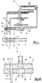
- a base plate connector has a plurality of long and thin terminals 3 which protrude from the rear face of a connector housing 2 and bend downwards.
- the anterior ends of the terminals 3 are aligned so as to fit with connecting holes H formed in a circuit board P. It is arranged so that, when attachment is carried out, the connector housing 2 is fixed at a specified position on the circuit board P, the anterior end of the terminals 3 being inserted into the connecting holes H and being fixed by means of soldering M.
- the connector housing 2 has an alignment plate 4 fixed thereon, this alignment plate 4 serving as a guide means for carrying out the insertion operation of the terminals 3 into the connecting hole H.
- the alignment plate 4 has position fixing holes 5 that correspond to the connecting holes H on the circuit base plate P. The anterior ends of the terminals 3 pass through the position fixing holes 5 and as a consequence the terminals 3 are positioned and aligned with the connecting holes H.
- the position fixing holes 5 are arranged to be of the minimum necessary size in order to prevent sideways movement of the terminals 3. For this reason, if a force applies so that the position fixing holes 5 shift in position with respect of the connecting holes H, this force is transmitted to the soldered portions M via the terminals 3, and stress on the soldered portions M increases.
- the present invention has been developed after taking the above problem into account, and aims to reduce stress on the soldered portions joining the terminals to the circuit board.
- a first embodiment 1 of the present invention is explained hereinbelow with reference to Figures 1 to 4.
- a circuit board connector C of the present embodiment has a connector housing 10, which is attached by making its lower face make contact with the surface of a circuit board P, the connector housing 10 then being fixed by means of a fixing means (not shown) such as screws or the like to a specified position on the circuit board P.
- a plurality of terminals 11 extend from the connector housing 10.
- Each terminal 11 protrudes from the rear face of the connector housing 10 and is bent in a downwards direction, its anterior end forming a right angle with respect to the lower face of the connector housing 10 and extending in a downward direction beyond the lower face.
- the anterior ends of these terminals 11 are arranged to be insertable simultaneously into connecting holes H of the circuit board P.
- the anterior ends of the terminals 11 are mutually parallel and the relative mutual alignment of the anterior ends of the terminals 11 is arranged to correspond to that of the connecting holes H of the circuit board P.
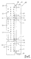
- the connector housing 10 further comprises an alignment plate 12 which has a main plate 13 and three attachment members 14 extending from the edges of the main plate 13. These attachment members 14 are fixed to the lower face of the connector housing 10, the alignment plate 12 accordingly being fixed and attached to the connector housing 10.
- the main plate 13 has a plurality of position fixing holes 15 therethrough from the lower face through to the upper face thereof, the position fixing holes 15 being arranged so as to correspond to the connecting holes H of the circuit board P.
- the position fixing holes 15 have a rectangular shape so as to correspond to the cross-sectional shape of the terminals 11.
- the dimensions of the vertical and horizontal edges of the open ends of each position fixing hole 15 are set to be greater than that of the terminal 11, and supporting protrusions 16 are formed in the central portion of the edges of each open end.
- Each position fixing hole 15 allows a corresponding terminal 11 to pass therethrough.
- the mutual positioning of the terminals 11 is arranged to correspond to the alignment of the connecting holes H with a high degree of accuracy.
- the alignment plate 12 is attached to the connector housing 10 in the state where the terminals 11 are arranged as described above.
- each position fixing hole 15 is surrounded on its four sides by four throughholes 17, each throughhole 17 having a cross-section which is elongate with rounded ends. Each throughhole 17 is parallel to the respective side of the fixing hole 15. The region between each of the throughholes 17 and the position fixing hole 15 forms a bendable member 18.
- the portion which is bound by the four bendable members 18 and includes the position fixing hole 15 forms a movable region 19.
- this movable region 19 is arranged to move relative to the attachment members 14, accompanied by the resilient bending of the bendable members 18.
- the force required for bending the bendable member 18 is greater than the force required to correct the position displacement of the terminal 11, and is less than a force that would produce a crack in the portion M soldered with the circuit board P of the terminal 11.
- the terminals 11 and the alignment plate 12 are attached to the connector housing 10. This operation is carried out by causing the alignment plate 12 to approach the terminals 11 from below and passing the terminals 11 into the position fixing holes 15. At this juncture, if there are any terminals 11 that are displaced from their true positions, the positions of these terminals 11 are corrected and they are fitted into the position fixing holes 15. Accordingly, the positioning of all the terminals 11 is made to correspond to the alignment of the connecting holes H with a high degree of accuracy. Thereafter, the alignment plate 12 is attached to the connector housing 10.
- the bendable member 18 possesses a certain amount of strength, and since the force capable of causing a resilient bending of the bendable member 18 is set to be greater than the force necessary to correct the position of the terminal 11 that has been dislocated, the bendable member 18 does not bend due to the recovery force of this terminal 11. As a result, the terminal 11 is fixed in position accurately.
- the connector C in which the attachment of the terminals 11 and the attachment plate 12 to the connector housing 10 has been completed, is then attached to the circuit board P.
- the anterior ends of the terminals 11, which have been aligned by means of the alignment plate 12, are inserted into the connecting holes H of the circuit board P.
- all the terminals 11 are aligned to correspond to the arrangement of the connecting holes H, all the terminals 11 simultaneously and smoothly enter the connecting holes H.
- the terminals 11 are pushed in further, thereby bringing the alignment plate 12 closer to the circuit board P.
- the connector housing 10 is fixed in a specified position on the circuit board P, and the portions of the terminals 11 that have been inserted into the connecting holes H are fixed by means of soldering M. In this way, the attachment of the base plate connector C to the circuit board P is completed.
- the movable region 19, which includes the position fixing holes 15, is arranged to be movable relative to the main plate 13, the attachment member 14 and the connector housing 10, the relative displacement of the alignment plate 12 and the circuit board P is accommodated due to the bending of the bendable member 18 (see Figure 4), and the position fixing holes 15 are maintained in a constant position with respect to the connecting holes H.
- the recovery force of the bendable member 18 applies to the terminals 11 via the protecting protrusions 16.
- the force that causes the bending of the bendable member 18 is set to be lower than a force that could cause a crack in the soldered portion, the integrity of the soldered connection M is maintained.
- the second embodiment differs from the first embodiment in that the configuration of the alignment plate is different. Since the second embodiment is the same as the first embodiment in all other respects, the same number as in the first embodiment is accorded to each similar part and an explanation of the configuration, operation and effect thereof is omitted.
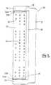
- An alignment plate 20 of the second embodiment comprises a long and narrow attachment member 21 which is attached to the base face of a connector housing 10 by being fixed thereto, and three sub-plates 23 (the movable region) which have position fixing holes 22 formed thereon.
- Each sub-plate 23 has a plurality of the position fixing holes 22 formed thereon, these position fixing holes 22 having the same alignment as connecting holes H provided on a circuit board P.
- Each position hole 22 is arranged to allow a respective terminal 11 to be fitted tightly therein.
- the sub-plates 23 are arranged to make contact so as to fit tightly with the surface of the circuit board P when they are in a fitted state with the circuit board P.
- the three sub-plates 23 are arranged along the lengthwise direction of the attachment member 21, and the mutually adjacent sub-plates 23 are connected in twos in a unified manner by two connecting members 24. Furthermore, the three sub-plates 23, which are formed integrally by means of these connecting members 24, are supported integrally by the attachment member 21 by means of four supporting members 25. Among these four supporting members 25, the two at the extreme ends are connected directly to the aligning plates 23, whilst the two medial supporting members 25 are connected to the connecting members 24.
- These supporting members 25 and connecting members 24 are arranged to be strong enough to support the sub-plates 23 without allowing them to bend too easily towards the attachment member 21. Moreover, the supporting members 25 and the connecting members 24 are arranged so as not to interfere with the terminals 11 on the face extending along the alignment plate 20.
- the circuit board P has receiving holes 26 that correspond to the supporting members 25 and the connecting members 24 when the base plate connector C is in an attached state to the circuit board P (see Figures 6 and 8).
- a cutter 27 cuts through the supporting members 25 and connecting members 24 (see Figures 6 and 8). As shown in Figure 10, the cutter 27 straddles the alignment plate 20 and is provided so as to correspond to the receiving holes 26. The cutter 27 cuts through the supporting member 25 of the connecting member 24 and enters the receiving hole 26.
- This cutter 27 has a cylindrical shape and its open end constitutes a sharp circular blade. Due to this, when the supporting member 25 and the connecting member 24 are cut through, a portion corresponding to the inner tubular shape of the cutter 27 remains uncut.
- the terminals 11 are inserted into the position fixing holes 22 and the attachment member 21 of the alignment plate 20 is fixed to the connector housing 10. At this juncture, if there is a dislocated terminal 11, its position is corrected and it is inserted into the position fixing hole 22. As a result, the positioning of all the terminals 11 comes to be aligned so as to correspond to a high degree to the alignment of the connecting holes H.
- the connector C is attached to the circuit board P.
- the anterior ends of the terminals 11 are inserted into the connecting holes H, and since at this juncture all the terminals 11 are arranged to correspond to the alignment of the connecting holes H, all the terminals 11 enter the connecting holes H simultaneously and smoothly.
- the terminals 11 are inserted, they are pushed in further so that the alignment plate 20 fits snugly with the circuit board P, and the connector housing 10 is fixed to a specified position on the circuit board plate P and is attached thereto.
- the cutter 27 is operated so as to cut through the supporting member 25 and the connecting member 24.
- a portion in the supporting member 25 and of the connecting member 24 corresponding to the inner tubular shape of the cutter 27 remains uncut and a space is formed respectively between residual portions 25A of the supporting members 25, between residual portions 24A of the connecting members 24, and between the residual portions 25A of the supporting member 25 and the residual portions 24A of the connecting members 24. Due to this space, relative movement parallel to the surface of the circuit board P becomes possible between the aligning plates 23 and between the sub-plates 23 and the attachment member 21.
- the second embodiment by separating the sub-plates 23, which have the position fixing holes 22 formed thereon, from the attachment member 21, and allowing the sub-plates 23 to move, the dislocation of the position fixing holes 22 with respect to the connecting holes H is prevented. Accordingly, increase in stress on the soldered portion M resulting from the dislocation of the position fixing holes 22 with respect to the connecting holes H is prevented.
- the present embodiment differs from the first embodiment in that the configuration of the alignment plate is different. Since the third embodiment is the same as the first embodiment in all other respects, the same number as in the first embodiment is accorded to each similar part and an explanation of the configuration, operation and effect thereof is omitted.
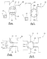
- An alignment plate 30 of the present embodiment comprises a long and narrow attachment member 31 which is attached to the base face of a connector housing 10 by being fixed thereto, and sub-plates 33 (the movable region) which have position fixing holes 32 formed thereon.
- the ends of the attachment member 31 have a pair of arm members 34 formed so as to project at a right angle to the lengthwise direction of the attachment member 31.
- the sub-plate 33 has the same thickness as the arm member 34, and, as shown in Figure 12, protrudes in a downward direction (towards the face facing the circuit board P) in a stepped shape, the stepped portion being approximately as thick as the thickness of the arm member 34.
- an inner side face 34A of the edge corresponding to the sub-plate 33 of the arm member 34 inclines so as to approach the sub-plate 33, in the direction of protrusion of the sub-plate 33.
- an external side face 33A of the edge corresponding to the arm member 34 of the sub-plate 33 inclines by the same angle and in the same direction as the edge of this corresponding arm member 34.
- the lower edge of the inner side face 34A of the arm member 34 and the upper edge of the outer side face 33A of the sub-plate 33 approach each other mutually.
- These edges are connected in a unified manner by means of a supporting member 35. Due to the supporting member 35 the sub-plate 33 is supported by the attachment member 31 via the arm member 34. Furthermore, a long and narrow space 36 is formed between the sub-plate 33 and the attachment member 31 along their lengthwise direction.
- the supporting member 35 has sufficient strength to hold the sub-plate 33 in a specified supported position with respect to the arm member 34. However, if a force greater than a specified amount is applied in a direction perpendicular to the face of the alignment plate 30 (that is, the attachment direction with respect to the circuit board P), the supporting member 35 is designed to break.
- the sub-plate 33 has a plurality of position fixing holes 32 arranged so as to correspond to the connecting holes H of the circuit board P, as in the case of the second embodiment.
- the terminals 11 are aligned so as to correspond to the connecting holes H.
- the terminals 11 are aligned by being inserted into the position fixing holes 32 and the attachment member 31 of the alignment plate 30 is fixed to the connector housing 10. After this, the connector C is attached to the circuit board P. During attachment, first the anterior ends of the terminals 11 are inserted into the connecting holes H, and since at this juncture all the terminals 11 are arranged to correspond to the alignment of the connecting holes H, all the terminals 11 enter the connecting holes H simultaneously and smoothly.
- the anterior ends of the terminals 11 are inserted, they are pushed in further and the connector housing 10 is brought closer to the circuit board P so that the lower face of the sub-plate 33 makes contact with the circuit board P. From this state, when the connector housing 10 is pushed further into the circuit board P, a pushing force is applied from the circuit board P towards the sub-plate 33. Due to this force the supporting members 35 break and sub-plate 33 separates from the arm member 33. The separated sub-plate 33 thus comes to be housed within the arm members 34. After this, the position of the connector housing 10 is fixed to a specified location on the circuit board P, and portions of the terminals 11 that have been inserted into the connecting holes H are fixed by means of soldering M. This completes the attachment operation of the connector C to the circuit board.
- the sub-plate 33 is separated from the attachment member 31. Moreover, since the external side face 33A of the sub-plate 3 and the inner side face 34A of the arm member are inclined in the same direction, a space 37 is maintained between them, this space 37 allowing movement relative to each other in the approaching and separating directions. Furthermore, since between the sub-plate 33 and the attachment member 31 the space 38 is maintained from the very beginning, movement in the approaching and separating directions of the sub-plate 33 and the attachment member 31 is permitted.
- the dislocation of the position fixing holes 32 with respect to the connecting holes H is prevented. Accordingly, increase in stress on the soldered portion M resulting from the dislocation of the position fixing holes 32 with respect to the connecting holes I is prevented.
- the present embodiment differs from the third embodiment 3 in that a portion of the configuration of the alignment plate is different. Since the fourth embodiment is the same as the third embodiment in all other respects, the same number as in the third embodiment is accorded to each similar part and an explanation of the configuration, operation and effect thereof is omitted.
- a supporting member 35 that connects an arm member 34 of an attachment member 31 and a sub-plate 33 is provided partially along the lengthwise direction of edges 33A and 34A.
- the portion between the arm member 34 and the sub-plate 33 that does not have the supporting member 35 has an elastically bendable, thin, flat hinge 40 formed in a bent shape.
- One end of this hinge 40 protrudes from a position located close to the edge 34A on the upper face of the arm member 34, the other end of the hinge 40 protruding from a position located close to the edge 33A on the upper face of the sub-plate 33.
- This hinge 40 connects the arm member 34 and the sub-plate 33.
- the hinge 40 gets elastically bent. Due to the elastic recovery force of the hinge 40, the sub-plate 33 is pressed towards the circuit board P. Due to this pressing operation, the sub-plate 33 is prevented from excessively moving sideways or vertically along the terminals 11. Further, in this state, in the case where a force is applied so as to cause movement between the aligning plate 33 and the arm member 34 along the circuit base plate P, the hinge 40 elastically bends, thereby allowing mutual movement between the aligning plate 33 and the arm member 34. Consequently, there is no adverse effect on the prevention of excessive increase in force applying on the soldered portion M due to provision of the hinge 40.
Landscapes
- Coupling Device And Connection With Printed Circuit (AREA)
- Connector Housings Or Holding Contact Members (AREA)
Applications Claiming Priority (2)
| Application Number | Priority Date | Filing Date | Title |
|---|---|---|---|
| JP08105518A JP3104616B2 (ja) | 1996-04-25 | 1996-04-25 | 基板用コネクタ |
| JP105518/96 | 1996-04-25 |
Publications (2)
| Publication Number | Publication Date |
|---|---|
| EP0803940A2 true EP0803940A2 (de) | 1997-10-29 |
| EP0803940A3 EP0803940A3 (de) | 1998-05-27 |
Family
ID=14409829
Family Applications (1)
| Application Number | Title | Priority Date | Filing Date |
|---|---|---|---|
| EP97301624A Ceased EP0803940A3 (de) | 1996-04-25 | 1997-03-12 | Verbinder für Leiterplatte |
Country Status (4)
| Country | Link |
|---|---|
| US (1) | US5921789A (de) |
| EP (1) | EP0803940A3 (de) |
| JP (1) | JP3104616B2 (de) |
| CN (1) | CN1168008A (de) |
Cited By (2)
| Publication number | Priority date | Publication date | Assignee | Title |
|---|---|---|---|---|
| EP0918378A1 (de) * | 1997-11-19 | 1999-05-26 | Sumitomo Wiring Systems, Ltd. | Ein plattenförmiges Bauteil |
| WO2017036663A1 (de) * | 2015-09-04 | 2017-03-09 | Robert Bosch Gmbh | Steckerleiste mit einer ausrichtungsplatte für kontaktpins |
Families Citing this family (18)
| Publication number | Priority date | Publication date | Assignee | Title |
|---|---|---|---|---|
| TW354683U (en) * | 1997-12-31 | 1999-03-11 | Hon Hai Prec Ind Co Ltd | Battery connector |
| US6171116B1 (en) * | 1999-03-26 | 2001-01-09 | Delphi Technologies, Inc. | Pin terminal alignment system |
| US6494724B1 (en) | 2001-10-02 | 2002-12-17 | Molex Incorporated | Electrical connector with terminal tail aligning device |
| US7097494B1 (en) * | 2005-02-10 | 2006-08-29 | Lear Corporation | Alignment plate |
| JP4121538B1 (ja) * | 2007-03-12 | 2008-07-23 | タイコエレクトロニクスアンプ株式会社 | アライメントプレートおよび電気コネクタ |
| JP4830957B2 (ja) * | 2007-04-16 | 2011-12-07 | トヨタ自動車株式会社 | タインプレート及びこれを用いたコネクタ |
| JP2009129778A (ja) * | 2007-11-26 | 2009-06-11 | Sumitomo Wiring Syst Ltd | 基板用コネクタ及び電気接続箱 |
| JP4914848B2 (ja) * | 2008-02-08 | 2012-04-11 | 矢崎総業株式会社 | アライニングプレート付きコネクタ |
| CN101997214B (zh) * | 2009-08-26 | 2013-01-02 | 合兴集团汽车电子有限公司 | 汽车发动机控制模块连接器总成的加工方法 |
| CN201829689U (zh) * | 2010-06-08 | 2011-05-11 | 富士康(昆山)电脑接插件有限公司 | 电连接器 |
| DE102010043495B4 (de) * | 2010-11-05 | 2021-09-30 | Te Connectivity Germany Gmbh | Elektrisches Bauteil zur Oberflächenmontage |
| JP6325880B2 (ja) * | 2014-04-24 | 2018-05-16 | 矢崎総業株式会社 | コネクタ |
| WO2015163434A1 (ja) | 2014-04-24 | 2015-10-29 | 矢崎総業株式会社 | コネクタ |
| JP6842230B2 (ja) * | 2015-03-30 | 2021-03-17 | 矢崎総業株式会社 | コネクタ |
| CN110366876B (zh) * | 2017-03-06 | 2023-05-05 | 三菱电机株式会社 | 具有压配结构的控制单元 |
| CN111047974B (zh) * | 2019-12-11 | 2021-11-02 | 深圳市洲明科技股份有限公司 | 连接结构、连接组件和显示屏 |
| JP7240616B2 (ja) * | 2020-09-24 | 2023-03-16 | 住友電装株式会社 | コネクタ |
| JP2024107885A (ja) * | 2023-01-30 | 2024-08-09 | 住友電装株式会社 | コネクタ |
Family Cites Families (10)
| Publication number | Priority date | Publication date | Assignee | Title |
|---|---|---|---|---|
| US4056300A (en) * | 1973-02-20 | 1977-11-01 | Gte Sylvania Incorporated | Terminal connector with stress relief |
| JPS62136784A (ja) * | 1985-12-10 | 1987-06-19 | 菱星電装株式会社 | コネクタの端子位置決め機構 |
| JPH04119973A (ja) * | 1990-09-11 | 1992-04-21 | Dainippon Ink & Chem Inc | 接着された炭素質成形品の製造法 |
| JPH074782Y2 (ja) * | 1990-09-17 | 1995-02-01 | ヒロセ電機株式会社 | 電気コネクタ構造 |
| JPH0574524A (ja) * | 1991-04-02 | 1993-03-26 | Canon Inc | 回路基板用コネクタ及びこれを用いた基板と装置 |
| JP3008727B2 (ja) * | 1993-04-07 | 2000-02-14 | 住友電装株式会社 | 二重成型品 |
| JP2797177B2 (ja) * | 1995-01-20 | 1998-09-17 | モレックス インコーポレーテッド | 電気コネクタ |
| US5676554A (en) * | 1995-03-28 | 1997-10-14 | Sumitomo Wiring Systems, Ltd. | Board mounted connector |
| US5733143A (en) * | 1995-09-20 | 1998-03-31 | Thomas & Betts Corporation | Stacked electrical connector assembly |
| US5688129A (en) * | 1995-11-21 | 1997-11-18 | Flaherty; Roger J. | Electrical connector with lead positioning comb |
-
1996
- 1996-04-25 JP JP08105518A patent/JP3104616B2/ja not_active Expired - Fee Related
-
1997
- 1997-03-12 EP EP97301624A patent/EP0803940A3/de not_active Ceased
- 1997-03-27 US US08/825,182 patent/US5921789A/en not_active Expired - Lifetime
- 1997-04-24 CN CN97111730A patent/CN1168008A/zh active Pending
Cited By (4)
| Publication number | Priority date | Publication date | Assignee | Title |
|---|---|---|---|---|
| EP0918378A1 (de) * | 1997-11-19 | 1999-05-26 | Sumitomo Wiring Systems, Ltd. | Ein plattenförmiges Bauteil |
| US5908330A (en) * | 1997-11-19 | 1999-06-01 | Sumitomo Wiring Systems, Ltd. | Platelike member |
| WO2017036663A1 (de) * | 2015-09-04 | 2017-03-09 | Robert Bosch Gmbh | Steckerleiste mit einer ausrichtungsplatte für kontaktpins |
| DE102015217026B4 (de) | 2015-09-04 | 2021-11-25 | Robert Bosch Gmbh | Steckerleiste mit einer Ausrichtungsplatte für Kontaktpins |
Also Published As
| Publication number | Publication date |
|---|---|
| CN1168008A (zh) | 1997-12-17 |
| US5921789A (en) | 1999-07-13 |
| EP0803940A3 (de) | 1998-05-27 |
| JPH09293573A (ja) | 1997-11-11 |
| JP3104616B2 (ja) | 2000-10-30 |
Similar Documents
| Publication | Publication Date | Title |
|---|---|---|
| US5921789A (en) | Connector for a circuit board | |
| EP0810697B1 (de) | Verbinder für Leiterplatte | |
| US5895286A (en) | Terminal for electrical installations | |
| JP3930857B2 (ja) | 装置に実装された可撓性コネクタカバー組み立て体 | |
| KR100267161B1 (ko) | 전기통신케이블용 콘넥터구조 | |
| JPH10134909A (ja) | コネクタ | |
| JPH0463560B2 (de) | ||
| JPH02309577A (ja) | 回路板エッジコネクタ | |
| EP1014509A1 (de) | Ausrichtungsfehler ausgleichender Verbinder | |
| EP0821447B1 (de) | Verbinder für Leiterplatte | |
| EP0707325B1 (de) | Sicherungshalterung mit Aufnahmekontaktfedern für Leiterplattenmontage | |
| JP3312192B2 (ja) | 光ファイバの保持構造、及び光コネクタ | |
| JPH04149974A (ja) | コネクタ装置 | |
| US5938463A (en) | Socket for printed circuit boards | |
| EP0886349B1 (de) | Einseitiger Leiterplattenverbinder mit Gabelmontage | |
| JPH0757825A (ja) | コネクタ | |
| EP1497893B1 (de) | Lagehalter für verbinder | |
| JPH02172166A (ja) | 電気コネクタとプリント配線基板との取付構造 | |
| US4706350A (en) | Self-locating, self-fixturing hard crystal blank mounting system | |
| US11133608B2 (en) | Contact member for an IDC terminal, contact member assembly, set of contact members and housing comprising a contact member | |
| KR100303412B1 (ko) | 프린트기판용커넥터 | |
| JPH0785933A (ja) | 可動型電気コネクタ | |
| EP0723310A2 (de) | Verbessertes System für selectiv-wirksame elektrische Verbindung zwischen mehreren Stellen in einer Gehäuse | |
| JPH0434880A (ja) | コネクタ | |
| JP4073874B2 (ja) | コネクタ |
Legal Events
| Date | Code | Title | Description |
|---|---|---|---|
| PUAI | Public reference made under article 153(3) epc to a published international application that has entered the european phase |
Free format text: ORIGINAL CODE: 0009012 |
|
| 17P | Request for examination filed |
Effective date: 19970327 |
|
| AK | Designated contracting states |
Kind code of ref document: A2 Designated state(s): DE FR GB |
|
| PUAL | Search report despatched |
Free format text: ORIGINAL CODE: 0009013 |
|
| AK | Designated contracting states |
Kind code of ref document: A3 Designated state(s): DE FR GB |
|
| 17Q | First examination report despatched |
Effective date: 20000314 |
|
| GRAG | Despatch of communication of intention to grant |
Free format text: ORIGINAL CODE: EPIDOS AGRA |
|
| STAA | Information on the status of an ep patent application or granted ep patent |
Free format text: STATUS: THE APPLICATION HAS BEEN REFUSED |
|
| 18R | Application refused |
Effective date: 20021102 |