EP0801422A2 - Reinigungsmittelzusammensetzung für Photoresist und Verfahren zur Herstellung eines halbleitenden integrierten Schaltkreises - Google Patents
Reinigungsmittelzusammensetzung für Photoresist und Verfahren zur Herstellung eines halbleitenden integrierten Schaltkreises Download PDFInfo
- Publication number
- EP0801422A2 EP0801422A2 EP97105547A EP97105547A EP0801422A2 EP 0801422 A2 EP0801422 A2 EP 0801422A2 EP 97105547 A EP97105547 A EP 97105547A EP 97105547 A EP97105547 A EP 97105547A EP 0801422 A2 EP0801422 A2 EP 0801422A2
- Authority
- EP
- European Patent Office
- Prior art keywords
- photoresist
- layer
- inorganic substrate
- removing agent
- agent composition
- Prior art date
- Legal status (The legal status is an assumption and is not a legal conclusion. Google has not performed a legal analysis and makes no representation as to the accuracy of the status listed.)
- Granted
Links
- 229920002120 photoresistant polymer Polymers 0.000 title claims abstract description 63
- 239000004065 semiconductor Substances 0.000 title claims abstract description 22
- 238000000034 method Methods 0.000 title claims abstract description 21
- 239000000203 mixture Substances 0.000 title claims abstract description 20
- 239000003795 chemical substances by application Substances 0.000 claims abstract description 34
- 239000000758 substrate Substances 0.000 claims abstract description 27
- 125000001453 quaternary ammonium group Chemical group 0.000 claims abstract description 12
- XLYOFNOQVPJJNP-UHFFFAOYSA-N water Substances O XLYOFNOQVPJJNP-UHFFFAOYSA-N 0.000 claims abstract description 12
- 239000000908 ammonium hydroxide Substances 0.000 claims abstract description 11
- 230000000269 nucleophilic effect Effects 0.000 claims abstract description 8
- 150000005846 sugar alcohols Chemical class 0.000 claims abstract description 8
- 230000033116 oxidation-reduction process Effects 0.000 claims abstract description 6
- 150000001412 amines Chemical class 0.000 claims abstract description 4
- 125000004432 carbon atom Chemical group C* 0.000 claims description 12
- 125000000217 alkyl group Chemical group 0.000 claims description 8
- 239000000463 material Substances 0.000 abstract description 11
- 238000001312 dry etching Methods 0.000 abstract description 10
- 238000004380 ashing Methods 0.000 abstract description 7
- WGTYBPLFGIVFAS-UHFFFAOYSA-M tetramethylammonium hydroxide Chemical compound [OH-].C[N+](C)(C)C WGTYBPLFGIVFAS-UHFFFAOYSA-M 0.000 description 38
- FBPFZTCFMRRESA-FSIIMWSLSA-N D-Glucitol Natural products OC[C@H](O)[C@H](O)[C@@H](O)[C@H](O)CO FBPFZTCFMRRESA-FSIIMWSLSA-N 0.000 description 20
- 239000000600 sorbitol Substances 0.000 description 20
- 235000010356 sorbitol Nutrition 0.000 description 20
- 230000000052 comparative effect Effects 0.000 description 18
- 238000005260 corrosion Methods 0.000 description 14
- 230000007797 corrosion Effects 0.000 description 14
- AVXURJPOCDRRFD-UHFFFAOYSA-N Hydroxylamine Chemical compound ON AVXURJPOCDRRFD-UHFFFAOYSA-N 0.000 description 13
- XAGFODPZIPBFFR-UHFFFAOYSA-N aluminium Chemical compound [Al] XAGFODPZIPBFFR-UHFFFAOYSA-N 0.000 description 13
- 229910052782 aluminium Inorganic materials 0.000 description 13
- OAKJQQAXSVQMHS-UHFFFAOYSA-N Hydrazine Chemical compound NN OAKJQQAXSVQMHS-UHFFFAOYSA-N 0.000 description 12
- 235000011114 ammonium hydroxide Nutrition 0.000 description 10
- -1 naphthalene Chemical class 0.000 description 10
- 239000003960 organic solvent Substances 0.000 description 7
- LFQSCWFLJHTTHZ-UHFFFAOYSA-N Ethanol Chemical compound CCO LFQSCWFLJHTTHZ-UHFFFAOYSA-N 0.000 description 6
- HEBKCHPVOIAQTA-UHFFFAOYSA-N meso ribitol Natural products OCC(O)C(O)C(O)CO HEBKCHPVOIAQTA-UHFFFAOYSA-N 0.000 description 6
- 230000002378 acidificating effect Effects 0.000 description 5
- OEYIOHPDSNJKLS-UHFFFAOYSA-N choline Chemical compound C[N+](C)(C)CCO OEYIOHPDSNJKLS-UHFFFAOYSA-N 0.000 description 5
- 229960001231 choline Drugs 0.000 description 5
- ISWSIDIOOBJBQZ-UHFFFAOYSA-N Phenol Chemical compound OC1=CC=CC=C1 ISWSIDIOOBJBQZ-UHFFFAOYSA-N 0.000 description 4
- TVXBFESIOXBWNM-UHFFFAOYSA-N Xylitol Natural products OCCC(O)C(O)C(O)CCO TVXBFESIOXBWNM-UHFFFAOYSA-N 0.000 description 4
- 150000001875 compounds Chemical class 0.000 description 4
- 150000002429 hydrazines Chemical class 0.000 description 4
- 150000002443 hydroxylamines Chemical class 0.000 description 4
- 150000003839 salts Chemical class 0.000 description 4
- 239000000811 xylitol Substances 0.000 description 4
- 235000010447 xylitol Nutrition 0.000 description 4
- HEBKCHPVOIAQTA-SCDXWVJYSA-N xylitol Chemical compound OC[C@H](O)[C@@H](O)[C@H](O)CO HEBKCHPVOIAQTA-SCDXWVJYSA-N 0.000 description 4
- 229960002675 xylitol Drugs 0.000 description 4
- QVGXLLKOCUKJST-UHFFFAOYSA-N atomic oxygen Chemical compound [O] QVGXLLKOCUKJST-UHFFFAOYSA-N 0.000 description 3
- 238000004140 cleaning Methods 0.000 description 3
- HDZGCSFEDULWCS-UHFFFAOYSA-N monomethylhydrazine Chemical compound CNN HDZGCSFEDULWCS-UHFFFAOYSA-N 0.000 description 3
- 239000001301 oxygen Substances 0.000 description 3
- 229910052760 oxygen Inorganic materials 0.000 description 3
- 239000000243 solution Substances 0.000 description 3
- RHUYHJGZWVXEHW-UHFFFAOYSA-N 1,1-Dimethyhydrazine Chemical compound CN(C)N RHUYHJGZWVXEHW-UHFFFAOYSA-N 0.000 description 2
- RJFMDYQCCOOZHJ-UHFFFAOYSA-L 2-hydroxyethyl(trimethyl)azanium dihydroxide Chemical compound [OH-].[OH-].C[N+](C)(C)CCO.C[N+](C)(C)CCO RJFMDYQCCOOZHJ-UHFFFAOYSA-L 0.000 description 2
- KIZQNNOULOCVDM-UHFFFAOYSA-M 2-hydroxyethyl(trimethyl)azanium;hydroxide Chemical compound [OH-].C[N+](C)(C)CCO KIZQNNOULOCVDM-UHFFFAOYSA-M 0.000 description 2
- IJGRMHOSHXDMSA-UHFFFAOYSA-N Atomic nitrogen Chemical compound N#N IJGRMHOSHXDMSA-UHFFFAOYSA-N 0.000 description 2
- RYGMFSIKBFXOCR-UHFFFAOYSA-N Copper Chemical compound [Cu] RYGMFSIKBFXOCR-UHFFFAOYSA-N 0.000 description 2
- FBPFZTCFMRRESA-KVTDHHQDSA-N D-Mannitol Chemical compound OC[C@@H](O)[C@@H](O)[C@H](O)[C@H](O)CO FBPFZTCFMRRESA-KVTDHHQDSA-N 0.000 description 2
- FBPFZTCFMRRESA-JGWLITMVSA-N D-glucitol Chemical compound OC[C@H](O)[C@@H](O)[C@H](O)[C@H](O)CO FBPFZTCFMRRESA-JGWLITMVSA-N 0.000 description 2
- WQZGKKKJIJFFOK-QTVWNMPRSA-N D-mannopyranose Chemical compound OC[C@H]1OC(O)[C@@H](O)[C@@H](O)[C@@H]1O WQZGKKKJIJFFOK-QTVWNMPRSA-N 0.000 description 2
- SRBFZHDQGSBBOR-IOVATXLUSA-N D-xylopyranose Chemical compound O[C@@H]1COC(O)[C@H](O)[C@H]1O SRBFZHDQGSBBOR-IOVATXLUSA-N 0.000 description 2
- IAZDPXIOMUYVGZ-UHFFFAOYSA-N Dimethylsulphoxide Chemical compound CS(C)=O IAZDPXIOMUYVGZ-UHFFFAOYSA-N 0.000 description 2
- UNXHWFMMPAWVPI-UHFFFAOYSA-N Erythritol Natural products OCC(O)C(O)CO UNXHWFMMPAWVPI-UHFFFAOYSA-N 0.000 description 2
- WQZGKKKJIJFFOK-GASJEMHNSA-N Glucose Natural products OC[C@H]1OC(O)[C@H](O)[C@@H](O)[C@@H]1O WQZGKKKJIJFFOK-GASJEMHNSA-N 0.000 description 2
- PEDCQBHIVMGVHV-UHFFFAOYSA-N Glycerol Natural products OCC(O)CO PEDCQBHIVMGVHV-UHFFFAOYSA-N 0.000 description 2
- 229930195725 Mannitol Natural products 0.000 description 2
- UFWIBTONFRDIAS-UHFFFAOYSA-N Naphthalene Chemical compound C1=CC=CC2=CC=CC=C21 UFWIBTONFRDIAS-UHFFFAOYSA-N 0.000 description 2
- 239000002253 acid Substances 0.000 description 2
- 125000003342 alkenyl group Chemical group 0.000 description 2
- 125000003282 alkyl amino group Chemical group 0.000 description 2
- 125000000304 alkynyl group Chemical group 0.000 description 2
- WQZGKKKJIJFFOK-PHYPRBDBSA-N alpha-D-galactose Chemical compound OC[C@H]1O[C@H](O)[C@H](O)[C@@H](O)[C@H]1O WQZGKKKJIJFFOK-PHYPRBDBSA-N 0.000 description 2
- MTHSVFCYNBDYFN-UHFFFAOYSA-N anhydrous diethylene glycol Natural products OCCOCCO MTHSVFCYNBDYFN-UHFFFAOYSA-N 0.000 description 2
- PYMYPHUHKUWMLA-UHFFFAOYSA-N arabinose Natural products OCC(O)C(O)C(O)C=O PYMYPHUHKUWMLA-UHFFFAOYSA-N 0.000 description 2
- SRBFZHDQGSBBOR-UHFFFAOYSA-N beta-D-Pyranose-Lyxose Natural products OC1COC(O)C(O)C1O SRBFZHDQGSBBOR-UHFFFAOYSA-N 0.000 description 2
- WQZGKKKJIJFFOK-VFUOTHLCSA-N beta-D-glucose Chemical compound OC[C@H]1O[C@@H](O)[C@H](O)[C@@H](O)[C@@H]1O WQZGKKKJIJFFOK-VFUOTHLCSA-N 0.000 description 2
- 230000015572 biosynthetic process Effects 0.000 description 2
- 125000003178 carboxy group Chemical group [H]OC(*)=O 0.000 description 2
- 239000010949 copper Substances 0.000 description 2
- 229910052802 copper Inorganic materials 0.000 description 2
- 125000000753 cycloalkyl group Chemical group 0.000 description 2
- 230000000694 effects Effects 0.000 description 2
- 238000005530 etching Methods 0.000 description 2
- 238000011156 evaluation Methods 0.000 description 2
- 229930182830 galactose Natural products 0.000 description 2
- 239000008103 glucose Substances 0.000 description 2
- 238000010438 heat treatment Methods 0.000 description 2
- 125000004435 hydrogen atom Chemical group [H]* 0.000 description 2
- 239000000594 mannitol Substances 0.000 description 2
- 235000010355 mannitol Nutrition 0.000 description 2
- VDZOOKBUILJEDG-UHFFFAOYSA-M tetrabutylammonium hydroxide Chemical compound [OH-].CCCC[N+](CCCC)(CCCC)CCCC VDZOOKBUILJEDG-UHFFFAOYSA-M 0.000 description 2
- JIRHAGAOHOYLNO-UHFFFAOYSA-N (3-cyclopentyloxy-4-methoxyphenyl)methanol Chemical compound COC1=CC=C(CO)C=C1OC1CCCC1 JIRHAGAOHOYLNO-UHFFFAOYSA-N 0.000 description 1
- VTIRNZBEJBPYCV-UHFFFAOYSA-N 1-hydrazinylethanol Chemical compound CC(O)NN VTIRNZBEJBPYCV-UHFFFAOYSA-N 0.000 description 1
- FVRSWMRVYMPTBU-UHFFFAOYSA-M 1-hydroxypropyl(trimethyl)azanium;hydroxide Chemical compound [OH-].CCC(O)[N+](C)(C)C FVRSWMRVYMPTBU-UHFFFAOYSA-M 0.000 description 1
- LBLYYCQCTBFVLH-UHFFFAOYSA-N 2-Methylbenzenesulfonic acid Chemical compound CC1=CC=CC=C1S(O)(=O)=O LBLYYCQCTBFVLH-UHFFFAOYSA-N 0.000 description 1
- ZFDNAYFXBJPPEB-UHFFFAOYSA-M 2-hydroxyethyl(tripropyl)azanium;hydroxide Chemical compound [OH-].CCC[N+](CCC)(CCC)CCO ZFDNAYFXBJPPEB-UHFFFAOYSA-M 0.000 description 1
- 229910000838 Al alloy Inorganic materials 0.000 description 1
- JBRZTFJDHDCESZ-UHFFFAOYSA-N AsGa Chemical compound [As]#[Ga] JBRZTFJDHDCESZ-UHFFFAOYSA-N 0.000 description 1
- ZAMOUSCENKQFHK-UHFFFAOYSA-N Chlorine atom Chemical compound [Cl] ZAMOUSCENKQFHK-UHFFFAOYSA-N 0.000 description 1
- WQZGKKKJIJFFOK-CBPJZXOFSA-N D-Gulose Chemical compound OC[C@H]1OC(O)[C@H](O)[C@H](O)[C@H]1O WQZGKKKJIJFFOK-CBPJZXOFSA-N 0.000 description 1
- WQZGKKKJIJFFOK-WHZQZERISA-N D-aldose Chemical compound OC[C@H]1OC(O)[C@@H](O)[C@@H](O)[C@H]1O WQZGKKKJIJFFOK-WHZQZERISA-N 0.000 description 1
- WQZGKKKJIJFFOK-IVMDWMLBSA-N D-allopyranose Chemical compound OC[C@H]1OC(O)[C@H](O)[C@H](O)[C@@H]1O WQZGKKKJIJFFOK-IVMDWMLBSA-N 0.000 description 1
- LKDRXBCSQODPBY-JDJSBBGDSA-N D-allulose Chemical compound OCC1(O)OC[C@@H](O)[C@@H](O)[C@H]1O LKDRXBCSQODPBY-JDJSBBGDSA-N 0.000 description 1
- FBPFZTCFMRRESA-KAZBKCHUSA-N D-altritol Chemical compound OC[C@@H](O)[C@H](O)[C@H](O)[C@H](O)CO FBPFZTCFMRRESA-KAZBKCHUSA-N 0.000 description 1
- HEBKCHPVOIAQTA-QWWZWVQMSA-N D-arabinitol Chemical compound OC[C@@H](O)C(O)[C@H](O)CO HEBKCHPVOIAQTA-QWWZWVQMSA-N 0.000 description 1
- FBPFZTCFMRRESA-ZXXMMSQZSA-N D-iditol Chemical compound OC[C@@H](O)[C@H](O)[C@@H](O)[C@H](O)CO FBPFZTCFMRRESA-ZXXMMSQZSA-N 0.000 description 1
- HMFHBZSHGGEWLO-SOOFDHNKSA-N D-ribofuranose Chemical compound OC[C@H]1OC(O)[C@H](O)[C@@H]1O HMFHBZSHGGEWLO-SOOFDHNKSA-N 0.000 description 1
- ZAQJHHRNXZUBTE-NQXXGFSBSA-N D-ribulose Chemical compound OC[C@@H](O)[C@@H](O)C(=O)CO ZAQJHHRNXZUBTE-NQXXGFSBSA-N 0.000 description 1
- UNXHWFMMPAWVPI-QWWZWVQMSA-N D-threitol Chemical compound OC[C@@H](O)[C@H](O)CO UNXHWFMMPAWVPI-QWWZWVQMSA-N 0.000 description 1
- ZAQJHHRNXZUBTE-UHFFFAOYSA-N D-threo-2-Pentulose Natural products OCC(O)C(O)C(=O)CO ZAQJHHRNXZUBTE-UHFFFAOYSA-N 0.000 description 1
- YTBSYETUWUMLBZ-QWWZWVQMSA-N D-threose Chemical compound OC[C@@H](O)[C@H](O)C=O YTBSYETUWUMLBZ-QWWZWVQMSA-N 0.000 description 1
- ZAQJHHRNXZUBTE-WUJLRWPWSA-N D-xylulose Chemical compound OC[C@@H](O)[C@H](O)C(=O)CO ZAQJHHRNXZUBTE-WUJLRWPWSA-N 0.000 description 1
- 229920001174 Diethylhydroxylamine Polymers 0.000 description 1
- 239000004386 Erythritol Substances 0.000 description 1
- IAYPIBMASNFSPL-UHFFFAOYSA-N Ethylene oxide Chemical compound C1CO1 IAYPIBMASNFSPL-UHFFFAOYSA-N 0.000 description 1
- 229930091371 Fructose Natural products 0.000 description 1
- RFSUNEUAIZKAJO-ARQDHWQXSA-N Fructose Chemical compound OC[C@H]1O[C@](O)(CO)[C@@H](O)[C@@H]1O RFSUNEUAIZKAJO-ARQDHWQXSA-N 0.000 description 1
- GPXJNWSHGFTCBW-UHFFFAOYSA-N Indium phosphide Chemical compound [In]#P GPXJNWSHGFTCBW-UHFFFAOYSA-N 0.000 description 1
- LKDRXBCSQODPBY-AMVSKUEXSA-N L-(-)-Sorbose Chemical compound OCC1(O)OC[C@H](O)[C@@H](O)[C@@H]1O LKDRXBCSQODPBY-AMVSKUEXSA-N 0.000 description 1
- WQZGKKKJIJFFOK-VSOAQEOCSA-N L-altropyranose Chemical compound OC[C@@H]1OC(O)[C@H](O)[C@@H](O)[C@H]1O WQZGKKKJIJFFOK-VSOAQEOCSA-N 0.000 description 1
- PYMYPHUHKUWMLA-LMVFSUKVSA-N Ribose Natural products OC[C@@H](O)[C@@H](O)[C@@H](O)C=O PYMYPHUHKUWMLA-LMVFSUKVSA-N 0.000 description 1
- VYPSYNLAJGMNEJ-UHFFFAOYSA-N Silicium dioxide Chemical compound O=[Si]=O VYPSYNLAJGMNEJ-UHFFFAOYSA-N 0.000 description 1
- RTAQQCXQSZGOHL-UHFFFAOYSA-N Titanium Chemical compound [Ti] RTAQQCXQSZGOHL-UHFFFAOYSA-N 0.000 description 1
- NRTOMJZYCJJWKI-UHFFFAOYSA-N Titanium nitride Chemical compound [Ti]#N NRTOMJZYCJJWKI-UHFFFAOYSA-N 0.000 description 1
- HMFHBZSHGGEWLO-UHFFFAOYSA-N alpha-D-Furanose-Ribose Natural products OCC1OC(O)C(O)C1O HMFHBZSHGGEWLO-UHFFFAOYSA-N 0.000 description 1
- 239000007864 aqueous solution Substances 0.000 description 1
- PYMYPHUHKUWMLA-WDCZJNDASA-N arabinose Chemical compound OC[C@@H](O)[C@@H](O)[C@H](O)C=O PYMYPHUHKUWMLA-WDCZJNDASA-N 0.000 description 1
- 150000004945 aromatic hydrocarbons Chemical class 0.000 description 1
- SRSXLGNVWSONIS-UHFFFAOYSA-N benzenesulfonic acid Chemical compound OS(=O)(=O)C1=CC=CC=C1 SRSXLGNVWSONIS-UHFFFAOYSA-N 0.000 description 1
- 229940092714 benzenesulfonic acid Drugs 0.000 description 1
- 239000000460 chlorine Substances 0.000 description 1
- 229910052801 chlorine Inorganic materials 0.000 description 1
- 238000000354 decomposition reaction Methods 0.000 description 1
- JQDCIBMGKCMHQV-UHFFFAOYSA-M diethyl(dimethyl)azanium;hydroxide Chemical compound [OH-].CC[N+](C)(C)CC JQDCIBMGKCMHQV-UHFFFAOYSA-M 0.000 description 1
- FVCOIAYSJZGECG-UHFFFAOYSA-N diethylhydroxylamine Chemical compound CCN(O)CC FVCOIAYSJZGECG-UHFFFAOYSA-N 0.000 description 1
- 238000005516 engineering process Methods 0.000 description 1
- 235000019414 erythritol Nutrition 0.000 description 1
- UNXHWFMMPAWVPI-ZXZARUISSA-N erythritol Chemical compound OC[C@H](O)[C@H](O)CO UNXHWFMMPAWVPI-ZXZARUISSA-N 0.000 description 1
- 229940009714 erythritol Drugs 0.000 description 1
- KVFVBPYVNUCWJX-UHFFFAOYSA-M ethyl(trimethyl)azanium;hydroxide Chemical compound [OH-].CC[N+](C)(C)C KVFVBPYVNUCWJX-UHFFFAOYSA-M 0.000 description 1
- LYCAIKOWRPUZTN-UHFFFAOYSA-N ethylene glycol Natural products OCCO LYCAIKOWRPUZTN-UHFFFAOYSA-N 0.000 description 1
- 229960002737 fructose Drugs 0.000 description 1
- FBPFZTCFMRRESA-GUCUJZIJSA-N galactitol Chemical compound OC[C@H](O)[C@@H](O)[C@@H](O)[C@H](O)CO FBPFZTCFMRRESA-GUCUJZIJSA-N 0.000 description 1
- 239000011521 glass Substances 0.000 description 1
- 150000004676 glycans Chemical class 0.000 description 1
- 150000002440 hydroxy compounds Chemical class 0.000 description 1
- WGCNASOHLSPBMP-UHFFFAOYSA-N hydroxyacetaldehyde Natural products OCC=O WGCNASOHLSPBMP-UHFFFAOYSA-N 0.000 description 1
- 125000002951 idosyl group Chemical class C1([C@@H](O)[C@H](O)[C@@H](O)[C@H](O1)CO)* 0.000 description 1
- 238000007654 immersion Methods 0.000 description 1
- BJHIKXHVCXFQLS-PQLUHFTBSA-N keto-D-tagatose Chemical compound OC[C@@H](O)[C@H](O)[C@H](O)C(=O)CO BJHIKXHVCXFQLS-PQLUHFTBSA-N 0.000 description 1
- 239000007788 liquid Substances 0.000 description 1
- 150000002772 monosaccharides Chemical class 0.000 description 1
- VMESOKCXSYNAKD-UHFFFAOYSA-N n,n-dimethylhydroxylamine Chemical compound CN(C)O VMESOKCXSYNAKD-UHFFFAOYSA-N 0.000 description 1
- CPQCSJYYDADLCZ-UHFFFAOYSA-N n-methylhydroxylamine Chemical compound CNO CPQCSJYYDADLCZ-UHFFFAOYSA-N 0.000 description 1
- 229910052757 nitrogen Inorganic materials 0.000 description 1
- 229910052698 phosphorus Inorganic materials 0.000 description 1
- 239000011574 phosphorus Substances 0.000 description 1
- 229910021420 polycrystalline silicon Inorganic materials 0.000 description 1
- 229920001282 polysaccharide Polymers 0.000 description 1
- 239000005017 polysaccharide Substances 0.000 description 1
- 229920005591 polysilicon Polymers 0.000 description 1
- HEBKCHPVOIAQTA-ZXFHETKHSA-N ribitol Chemical compound OC[C@H](O)[C@H](O)[C@H](O)CO HEBKCHPVOIAQTA-ZXFHETKHSA-N 0.000 description 1
- 229910052710 silicon Inorganic materials 0.000 description 1
- 239000010703 silicon Substances 0.000 description 1
- 229910052814 silicon oxide Inorganic materials 0.000 description 1
- 238000005507 spraying Methods 0.000 description 1
- 229940073455 tetraethylammonium hydroxide Drugs 0.000 description 1
- LRGJRHZIDJQFCL-UHFFFAOYSA-M tetraethylazanium;hydroxide Chemical compound [OH-].CC[N+](CC)(CC)CC LRGJRHZIDJQFCL-UHFFFAOYSA-M 0.000 description 1
- LPSKDVINWQNWFE-UHFFFAOYSA-M tetrapropylazanium;hydroxide Chemical compound [OH-].CCC[N+](CCC)(CCC)CCC LPSKDVINWQNWFE-UHFFFAOYSA-M 0.000 description 1
- 239000010936 titanium Substances 0.000 description 1
- 229910052719 titanium Inorganic materials 0.000 description 1
- MAKDTFFYCIMFQP-UHFFFAOYSA-N titanium tungsten Chemical compound [Ti].[W] MAKDTFFYCIMFQP-UHFFFAOYSA-N 0.000 description 1
- HPWUYZIJILJHNG-UHFFFAOYSA-M tributyl(2-hydroxyethyl)azanium;hydroxide Chemical compound [OH-].CCCC[N+](CCO)(CCCC)CCCC HPWUYZIJILJHNG-UHFFFAOYSA-M 0.000 description 1
- GRNRCQKEBXQLAA-UHFFFAOYSA-M triethyl(2-hydroxyethyl)azanium;hydroxide Chemical compound [OH-].CC[N+](CC)(CC)CCO GRNRCQKEBXQLAA-UHFFFAOYSA-M 0.000 description 1
- WFKWXMTUELFFGS-UHFFFAOYSA-N tungsten Chemical compound [W] WFKWXMTUELFFGS-UHFFFAOYSA-N 0.000 description 1
- 229910052721 tungsten Inorganic materials 0.000 description 1
- 239000010937 tungsten Substances 0.000 description 1
- 229910021642 ultra pure water Inorganic materials 0.000 description 1
- 239000012498 ultrapure water Substances 0.000 description 1
Images
Classifications
-
- G—PHYSICS
- G03—PHOTOGRAPHY; CINEMATOGRAPHY; ANALOGOUS TECHNIQUES USING WAVES OTHER THAN OPTICAL WAVES; ELECTROGRAPHY; HOLOGRAPHY
- G03F—PHOTOMECHANICAL PRODUCTION OF TEXTURED OR PATTERNED SURFACES, e.g. FOR PRINTING, FOR PROCESSING OF SEMICONDUCTOR DEVICES; MATERIALS THEREFOR; ORIGINALS THEREFOR; APPARATUS SPECIALLY ADAPTED THEREFOR
- G03F7/00—Photomechanical, e.g. photolithographic, production of textured or patterned surfaces, e.g. printing surfaces; Materials therefor, e.g. comprising photoresists; Apparatus specially adapted therefor
- G03F7/26—Processing photosensitive materials; Apparatus therefor
- G03F7/42—Stripping or agents therefor
-
- H—ELECTRICITY
- H01—ELECTRIC ELEMENTS
- H01L—SEMICONDUCTOR DEVICES NOT COVERED BY CLASS H10
- H01L21/00—Processes or apparatus adapted for the manufacture or treatment of semiconductor or solid state devices or of parts thereof
- H01L21/02—Manufacture or treatment of semiconductor devices or of parts thereof
- H01L21/02041—Cleaning
- H01L21/02057—Cleaning during device manufacture
- H01L21/02068—Cleaning during device manufacture during, before or after processing of conductive layers, e.g. polysilicon or amorphous silicon layers
- H01L21/02071—Cleaning during device manufacture during, before or after processing of conductive layers, e.g. polysilicon or amorphous silicon layers the processing being a delineation, e.g. RIE, of conductive layers
-
- G—PHYSICS
- G03—PHOTOGRAPHY; CINEMATOGRAPHY; ANALOGOUS TECHNIQUES USING WAVES OTHER THAN OPTICAL WAVES; ELECTROGRAPHY; HOLOGRAPHY
- G03F—PHOTOMECHANICAL PRODUCTION OF TEXTURED OR PATTERNED SURFACES, e.g. FOR PRINTING, FOR PROCESSING OF SEMICONDUCTOR DEVICES; MATERIALS THEREFOR; ORIGINALS THEREFOR; APPARATUS SPECIALLY ADAPTED THEREFOR
- G03F7/00—Photomechanical, e.g. photolithographic, production of textured or patterned surfaces, e.g. printing surfaces; Materials therefor, e.g. comprising photoresists; Apparatus specially adapted therefor
- G03F7/26—Processing photosensitive materials; Apparatus therefor
- G03F7/42—Stripping or agents therefor
- G03F7/422—Stripping or agents therefor using liquids only
- G03F7/425—Stripping or agents therefor using liquids only containing mineral alkaline compounds; containing organic basic compounds, e.g. quaternary ammonium compounds; containing heterocyclic basic compounds containing nitrogen
-
- H—ELECTRICITY
- H01—ELECTRIC ELEMENTS
- H01L—SEMICONDUCTOR DEVICES NOT COVERED BY CLASS H10
- H01L21/00—Processes or apparatus adapted for the manufacture or treatment of semiconductor or solid state devices or of parts thereof
- H01L21/02—Manufacture or treatment of semiconductor devices or of parts thereof
- H01L21/027—Making masks on semiconductor bodies for further photolithographic processing not provided for in group H01L21/18 or H01L21/34
-
- H—ELECTRICITY
- H01—ELECTRIC ELEMENTS
- H01L—SEMICONDUCTOR DEVICES NOT COVERED BY CLASS H10
- H01L21/00—Processes or apparatus adapted for the manufacture or treatment of semiconductor or solid state devices or of parts thereof
- H01L21/02—Manufacture or treatment of semiconductor devices or of parts thereof
- H01L21/04—Manufacture or treatment of semiconductor devices or of parts thereof the devices having potential barriers, e.g. a PN junction, depletion layer or carrier concentration layer
- H01L21/18—Manufacture or treatment of semiconductor devices or of parts thereof the devices having potential barriers, e.g. a PN junction, depletion layer or carrier concentration layer the devices having semiconductor bodies comprising elements of Group IV of the Periodic Table or AIIIBV compounds with or without impurities, e.g. doping materials
- H01L21/30—Treatment of semiconductor bodies using processes or apparatus not provided for in groups H01L21/20 - H01L21/26
- H01L21/31—Treatment of semiconductor bodies using processes or apparatus not provided for in groups H01L21/20 - H01L21/26 to form insulating layers thereon, e.g. for masking or by using photolithographic techniques; After treatment of these layers; Selection of materials for these layers
- H01L21/3105—After-treatment
- H01L21/311—Etching the insulating layers by chemical or physical means
- H01L21/31127—Etching organic layers
- H01L21/31133—Etching organic layers by chemical means
Definitions
- the present invention relates to a removing agent composition used for removing a photoresist in a process for producing a semiconductor integrated circuit and to a process for producing a semiconductor integrated circuit.
- Semiconductor integrated circuits are produced by a process in which a photoresist is applied onto an inorganic substrate, a pattern is formed on the photoresist by exposure to light and subsequent development, the formed pattern on the photoresist is used as a mask, the portions of the inorganic substrate not masked by the pattern of the photoresist are etched to form fine circuits, and then the photoresist is removed from the inorganic substrate; or by a process in which, after fine circuits are formed by the same steps as those described, the photoresist is ashed, and remaining residues of the photoresist are removed from the inorganic substrate.
- the acidic removing agent examples include a removing agent comprising an arylsulfonc acid such as benzenesulfonic acid, toluenesulfonic acid, and xylenesulfonic acid, a phenol, and an organic solvent containing chlorine (United States Patent No. 3,582,401) and a removing agent comprising an aromatic hydrocarbon such as naphthalene, a phenol, and an arylsulfonic acid (Japanese Patent Application Laid-Open No. Showa 62(1987)-35357).
- a removing agent comprising an arylsulfonc acid such as benzenesulfonic acid, toluenesulfonic acid, and xylenesulfonic acid, a phenol, and an organic solvent containing chlorine
- a removing agent comprising an aromatic hydrocarbon such as naphthalene, a phenol, and an arylsulfonic acid
- alkaline removing agent examples include a removing agent comprising an addition product of ethylene oxide to an alkanolamine or a polyalkylenepolyamine, a sulfone compound, and a glycol monoalkyl ether (Japanese Patent Application Laid-Open No. Showa 62(1987)-49355), and a removing agent comprising dimethyl sulfoxide as the main component, a diethylene glycol monoalkyl ether, and an organic hydroxy compound containing nitrogen (Japanese Patent Application Laid-Open No. Showa 64(1989)-42653).
- alkaline removing agents dissociate with moisture absorbed during use to generate an amine and become alkaline. Therefore, when cleaning with an organic solvent, such as an alcohol, is not conducted between the removal of the photoresist and the cleaning with water, the product is alkaline at the time of the cleaning with water.
- the alkaline removing agents show a large corrosive effect to aluminum and copper which are frequently used as the wiring material for the formation of fine circuits. Therefore, these agents are not suitable for the fine works to which strict dimensional accuracy has been required in recent years.
- the alkaline removing agents it is necessary that the product obtained after the removal of the photoresist be rinsed with an organic solvent, such as an alcohol. This causes a drawback in that the process is more complicated.
- a removing agent which can easily remove films, layers, and residues of the photoresist and does not cause corrosion of the wiring material in the circuit is required.
- the present invention has the object of solving the above problems of the removing agents used in the conventional technology and providing a removing agent composition for a photoresist which can remove a layer of a photoresist applied onto an inorganic substrate, a layer of a photoresist remaining after dry etching of an inorganic substrate which is masked by the layer, or residues of a layer of a photoresist remaining after dry etching of an inorganic substrate which is masked by the layer and subsequent ashing of the layer easily at a low temperature in a short time, enables ultra-fine working without causing corrosion of the wiring material of the circuit at all, allows rinsing of the product obtained after the removal of the photoresist with water alone without rinsing with an organic solvent, such as an alcohol, and leads to producing a circuit with a high accuracy.
- an organic solvent such as an alcohol
- a removing agent composition comprising an aqueous solution containing a quaternary ammonium hydroxide, a nucleophilic amine compound having an oxidation-reduction potential, a sugar and/or a sugar alcohol enables removal of a photoresist easily at a low temperature in a short time in a process for producing semiconductor integrated circuits, and that the above composition exhibits a combination of the advantageous properties that the composition does not show any corrosive property, and no corrosion of the wiring material used in the circuit takes place and that the operation can be facilitated.
- the present invention provides: a removing agent composition for a photoresist comprising 0.01 to 20 % by weight of a quaternary ammonium hydroxide represented by the general formula [(R 1 ) 3 N-R] + ⁇ OH - (wherein R represents an alkyl group having 1 to 4 carbon atoms or a hydroxy-substituted alkyl group having 1 to 4 carbon atoms, and R 1 represents an alkyl group having 1 to 3 carbon atoms), 1 to 80 % by weight of a nucleophilic amine having an oxidation-reduction potential, 0.5 to 20 % by weight of a sugar and/or a sugar alcohol, and water in the remaining amount; and a process for producing a semiconductor integrated circuit comprising removing a photoresist applied onto an inorganic substrate by using the removing agent composition described above.
- a removing agent composition for a photoresist comprising 0.01 to 20 % by weight of a quaternary ammonium hydroxide represented by
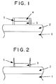
- Figure 1 shows a sectional view of a semiconductor integrated circuit obtained by forming a circuit of aluminum 3 by dry etching using a layer of a resist 4 as the mask.
- Figure 2 shows a sectional view of a semiconductor integrated circuit obtained by ashing the layer of a resist 4 in the semiconductor integrated circuit shown in Figure 1 with oxygen plasma to remove the layer of a resist 4.
- the quaternary ammonium hydroxide used in the present invention is represented by the general formula: [(R 1 ) 3 N-R] + ⁇ OH - (wherein R represents an alkyl group having 1 to 4 carbon atoms or a hydroxy-substituted alkyl group having 1 to 4 carbon atoms, and R 1 represents an alkyl group having 1 to 3 carbon atoms).
- Examples of the quaternary ammonium hydroxide represented by the above formula include tetramethylammonium hydroxide, tetraethylammonium hydroxide, tetrapropylammonium hydroxide, tetrabutylammonium hydroxide, trimethylethylammonium hydroxide, dimethyldiethylammonium hydroxide, trimethyl(2-hydroxyethyl)-ammonium hydroxide, triethyl(2-hydroxyethyl)ammonium hydroxide, tripropyl(2-hydroxyethyl)ammonium hydroxide, trimethyl(1-hydroxypropyl)ammonium hydroxide, and tributyl(2-hydroxyethyl)ammonium hydroxide.
- TMAH tetramethylammonium hydroxide
- choline trimethyl(2-hydroxyethyl)ammonium hydroxide
- the concentration of the quaternary ammonium hydroxide is 0.01 to 20 % by weight, preferably 0.1 to 10 % by weight, of the whole solution.
- concentration of the quaternary ammonium hydroxide is lower than the specified range, the speed of removal of the photoresist is low.
- concentration is higher than the specified range, corrosion of the wiring material in the circuit cannot be prevented.
- Examples of the nucleophilic amine compound having an oxidation-reduction potential which is used in combination with the quaternary ammonium hydroxide in the present invention include hydrazines represented by the general formula R 1 R 2 N-NR 3 R 4 (wherein R 1 , R 2 , R 3 , and R 4 represent each hydrogen atom or an alkyl group, a cycloalkyl group, an alkenyl group, an alkynyl group, a substituted carboxyl group, an alkylamino group, or a hydroxy-substituted alkyl group, each having 1 to 6 carbon atoms), derivatives of these hydrazines, salts of these hydrazines and derivatives of hydrazines, hydroxylamines represented by the general formula R 1 R 2 N-O-R 3 (wherein R 1 , R 2 , and R 3 represent each hydrogen atom or an alkyl group, a cycloalkyl group, an alkenyl group, an alky
- hydrazine examples include hydrazine, methylhydrazine, 1,1-dimethylhydrazine, hydrazinoethanol, and salts of these compounds.
- hydroxylamine examples include N-methylhydroxylamine, N,N-dimethylhydroxylamine, N,N-diethylhydroxylamine, and salts of these compounds.
- the concentration of the nucleophilic amine compound having an oxidation-reduction potential is in the range of 1 to 80 % by weight, preferably 3 to 40 % by weight, of the whole solution. When the concentration is lower than the specified range, the speed of removal of the photoresist is low.
- sugar used in the present invention examples include monosaccharides and polysaccharides.
- specific examples of the sugar include glycerol aldehydes having 3 to 6 carbon atoms, threose, arabinose, xylose, ribose, ribulose, xylulose, glucose, mannose, galactose, tagatose, allose, altrose, gulose, idose, talose, sorbose, psicose, and fruit sugar.
- sugar alcohol examples include threitol, erythritol, adonitol, arabitol, xylitol, talitol, sorbitol, mannitol, iditol, and dulcitol.
- glucose, mannose, galactose, sorbitol, mannitol, and xylitol are preferable in view of the solubility and the property of decomposition.
- the concentration of the sugar or the sugar alcohol is in the range of 0.5 to 20 % by weight, preferably 1 to 15 % by weight, of the whole solution.
- concentration of the sugar or the sugar alcohol is lower than the specified range, corrosion of the wiring material in the circuit cannot sufficiently be prevented.
- concentration is higher than the specified range, no additional advantage can be found, and the concentration is not preferable in view of the economy.
- Examples of the inorganic substrate used in the process for producing a semiconductor integrated circuit of the present invention include materials used for semiconductor circuits, such as silicon, polysilicon, silicon oxide films, aluminum, aluminum alloys, titanium, titanium-tungsten, titanium nitride, and tungsten; compound semiconductors, such as gallium-arsenic, gallium-phosphorus, and indium-phosphorus; and glass substrates of LCD.
- materials used for semiconductor circuits such as silicon, polysilicon, silicon oxide films, aluminum, aluminum alloys, titanium, titanium-tungsten, titanium nitride, and tungsten
- compound semiconductors such as gallium-arsenic, gallium-phosphorus, and indium-phosphorus
- glass substrates of LCD glass substrates of LCD.
- the removing agent composition for a photoresist of the present invention is used for removing a photoresist layer applied onto an inorganic substrate, a photoresist layer which is left remaining after dry etching of an inorganic substrate masked with a photoresist layer, or residues of a photoresist which are left remaining after dry etching of an inorganic substrate masked with a photoresist layer and subsequent ashing of the photoresist layer.
- heating or a treatment by ultrasonic wave may suitably be used in combination.
- the layer or the residues of the photoresist can sufficiently be removed at a room temperature. Heating or a treatment by ultrasonic wave may also be used in combination where necessary.
- the method of immersion is generally conducted in the treatment using the removing agent composition of the present invention.
- other methods such as the method of spraying, may also be used.
- the removing agent composition of the present invention When the removing agent composition of the present invention is used, it is not necessary that the product obtained after the removal of the photoresist is rinsed with an organic solvent, such as an alcohol. The rinsing with water alone is sufficient.
- a layer of a photoresist applied onto an inorganic substrate, a layer of a photoresist remaining after dry etching of an inorganic substrate which is masked by the layer, or residues of a layer of a photoresist remaining after dry etching of an inorganic substrate which is masked by the layer and subsequent ashing of the layer can be removed easily at a low temperature in a short time. Ultra-fine working is enabled without causing corrosion of the wiring material of the circuit at all.
- the product obtained after the removal of the photoresist can be rinsed with water alone, and rinsing with an organic solvent, such as an alcohol, is not necessary.
- Integrated circuits can be produced with a high accuracy. Therefore, in accordance with the process for producing a semiconductor integrated circuit of the present invention, integrated circuits having a high accuracy can very advantageously be produced industrially.
- Figure 1 shows a sectional view of a semiconductor integrated circuit obtained by forming a circuit of aluminum 3 by dry etching using a layer of a resist 4 as the mask.
- the substrate 1 of the semiconductor integrated circuit is coated with a layer of an oxide 2, and has layers at the sides 5 to protect the sides during the etching.
- Figure 2 shows a sectional view of a semiconductor integrated circuit obtained by ashing the layer of a resist 4 in the semiconductor integrated circuit shown in Figure 1 with oxygen plasma to remove the layer of a resist 4.
- the residues of the photoresist at the sides (the accumulated layers to protect the sides) 5 are left remaining without being removed by the oxygen plasma although the upper parts of the residues are deformed in such a manner that they are open with respect to the central line of the circuit of aluminum 3.
- the semiconductor integrated circuit shown in Figure 1 was immersed into a removing agent composition having a composition shown in Table 1 for a specified time. After being immersed, the integrated circuit was dried and observed under an electron microscope (SEM). The property for removal of the layer of a photoresist 4 and the residues of the photoresist 5 and the corrosion of the circuit of aluminum (AL) 3 were evaluated by the observation, and the results are shown in Table 1. The results of the evaluation are shown in accordance with the following classification:
- TMAH tetramethylammonium hydroxide
- Example 2 trimethyl(2-hydroxyethyl)ammonium hydroxide (choline) 10 hydrazine 15 sorbitol 10
- Example 3 choline 10 methylhydrazine 15 sorbitol 10
- Example 4 TMAH 10 hydroxylamine 15 sorbitol 10
- Example 5 choline 10 hydroxylamine 15 sorbitol 10
- Example 6 TMAH 10 hydroxylamine 15 xylitol 10
- Example 7 TMAH 15 hydroxylamine 10 sorbitol 15
- Example 8 TMAH 5 hydroxylamine 20 sorbitol 10 Comparative Example 1 TMAH 10 - - - - Comparative Example 2 TMAH 10 hydroxylamine 15 -
- the semiconductor integrated circuit shown in Figure 2 which had been treated by the ashing was immersed into a removing agent composition having a composition shown in Table 2 for a specified time. After being immersed, the integrated circuit was rinsed with ultra-pure water, dried, and observed under an electron microscope (SEM). The property for removal of the layer of a photoresist 4 and the residues of the photoresist 5 and the corrosion of the circuit of aluminum (AL) 3 were evaluated by the observation, and the results are shown in Table 2. The results of the evaluation are shown in accordance with the same classification as that used for the results shown in Table 1.
- TMAH tetramethylammonium hydroxide
- Example 10 trimethyl(2-hydroxyethyl)ammonium hydroxide (choline) 10 hydrazine 15 sorbitol 10
- Example 11 choline 10 methylhydrazine 15 sorbitol 10
- Example 12 TMAH 10 hydroxylamine 15 sorbitol 10
- Example 13 choline 10 hydroxylamine 15 sorbitol 10
- Example 15 TMAH 15 hydroxylamine 10 sorbitol 15 Example 16 TMAH 5 hydroxylamine 20 sorbitol 10 Comparative Example 5 TMAH 10 - - - - Comparative Example 6 TMAH 10 hydroxylamine 15 -
Landscapes
- Engineering & Computer Science (AREA)
- Physics & Mathematics (AREA)
- General Physics & Mathematics (AREA)
- Condensed Matter Physics & Semiconductors (AREA)
- Manufacturing & Machinery (AREA)
- Computer Hardware Design (AREA)
- Microelectronics & Electronic Packaging (AREA)
- Power Engineering (AREA)
- Chemical & Material Sciences (AREA)
- Chemical Kinetics & Catalysis (AREA)
- General Chemical & Material Sciences (AREA)
- Exposure Of Semiconductors, Excluding Electron Or Ion Beam Exposure (AREA)
- Photosensitive Polymer And Photoresist Processing (AREA)
- Cleaning Or Drying Semiconductors (AREA)
- Drying Of Semiconductors (AREA)
- Weting (AREA)
Applications Claiming Priority (3)
| Application Number | Priority Date | Filing Date | Title |
|---|---|---|---|
| JP09152196A JP3614242B2 (ja) | 1996-04-12 | 1996-04-12 | フォトレジスト剥離剤及び半導体集積回路の製造方法 |
| JP9152196 | 1996-04-12 | ||
| JP91521/96 | 1996-04-12 |
Publications (3)
| Publication Number | Publication Date |
|---|---|
| EP0801422A2 true EP0801422A2 (de) | 1997-10-15 |
| EP0801422A3 EP0801422A3 (de) | 1998-04-29 |
| EP0801422B1 EP0801422B1 (de) | 2002-12-18 |
Family
ID=14028728
Family Applications (1)
| Application Number | Title | Priority Date | Filing Date |
|---|---|---|---|
| EP97105547A Expired - Lifetime EP0801422B1 (de) | 1996-04-12 | 1997-04-03 | Reinigungsmittelzusammensetzung für Photoresist und Verfahren zur Herstellung eines halbleitenden integrierten Schaltkreises |
Country Status (9)
| Country | Link |
|---|---|
| US (1) | US5846695A (de) |
| EP (1) | EP0801422B1 (de) |
| JP (1) | JP3614242B2 (de) |
| KR (1) | KR100455299B1 (de) |
| DE (1) | DE69717900T2 (de) |
| ID (1) | ID16581A (de) |
| MY (1) | MY129085A (de) |
| SG (1) | SG76509A1 (de) |
| TW (1) | TW351830B (de) |
Cited By (3)
| Publication number | Priority date | Publication date | Assignee | Title |
|---|---|---|---|---|
| FR2793952A1 (fr) * | 1999-05-21 | 2000-11-24 | Commissariat Energie Atomique | Procede de realisation d'un niveau d'interconnexion de type damascene comprenant un dielectrique organique |
| WO2006050323A1 (en) * | 2004-10-29 | 2006-05-11 | Ekc Technology, Inc. | Compositions and processes for photoresist stripping and residue removal in wafer level packaging |
| US7543592B2 (en) | 2001-12-04 | 2009-06-09 | Ekc Technology, Inc. | Compositions and processes for photoresist stripping and residue removal in wafer level packaging |
Families Citing this family (17)
| Publication number | Priority date | Publication date | Assignee | Title |
|---|---|---|---|---|
| JPH1168095A (ja) * | 1997-08-11 | 1999-03-09 | Fujitsu Ltd | 半導体装置の製造方法 |
| US7547669B2 (en) | 1998-07-06 | 2009-06-16 | Ekc Technology, Inc. | Remover compositions for dual damascene system |
| US7135445B2 (en) * | 2001-12-04 | 2006-11-14 | Ekc Technology, Inc. | Process for the use of bis-choline and tris-choline in the cleaning of quartz-coated polysilicon and other materials |
| US7579308B2 (en) | 1998-07-06 | 2009-08-25 | Ekc/Dupont Electronics Technologies | Compositions and processes for photoresist stripping and residue removal in wafer level packaging |
| US6348239B1 (en) * | 2000-04-28 | 2002-02-19 | Simon Fraser University | Method for depositing metal and metal oxide films and patterned films |
| JP3410403B2 (ja) | 1999-09-10 | 2003-05-26 | 東京応化工業株式会社 | ホトレジスト用剥離液およびこれを用いたホトレジスト剥離方法 |
| KR100360985B1 (ko) | 2000-04-26 | 2002-11-18 | 주식회사 동진쎄미켐 | 레지스트 스트리퍼 조성물 |
| JP2002016034A (ja) * | 2000-06-30 | 2002-01-18 | Mitsubishi Electric Corp | 半導体装置の製造方法、及び半導体装置 |
| TWI295076B (en) * | 2002-09-19 | 2008-03-21 | Dongwoo Fine Chem Co Ltd | Washing liquid for semiconductor substrate and method of producing semiconductor device |
| US7199059B2 (en) * | 2004-10-26 | 2007-04-03 | United Microelectronics Corp. | Method for removing polymer as etching residue |
| US20060094612A1 (en) * | 2004-11-04 | 2006-05-04 | Mayumi Kimura | Post etch cleaning composition for use with substrates having aluminum |
| JP5224228B2 (ja) * | 2006-09-15 | 2013-07-03 | Nltテクノロジー株式会社 | 薬液を用いた基板処理方法 |
| US8900802B2 (en) | 2013-02-23 | 2014-12-02 | International Business Machines Corporation | Positive tone organic solvent developed chemically amplified resist |
| CN104678719A (zh) * | 2013-11-28 | 2015-06-03 | 安集微电子科技(上海)有限公司 | 一种对金属极低腐蚀的光刻胶清洗液 |
| JP5885041B1 (ja) * | 2014-10-27 | 2016-03-15 | パナソニックIpマネジメント株式会社 | レジスト剥離液 |
| JP5885046B1 (ja) * | 2015-03-24 | 2016-03-15 | パナソニックIpマネジメント株式会社 | レジスト剥離液 |
| CN107577121A (zh) * | 2017-08-29 | 2018-01-12 | 昆山艾森半导体材料有限公司 | 一种光刻胶去胶液 |
Citations (6)
| Publication number | Priority date | Publication date | Assignee | Title |
|---|---|---|---|---|
| EP0463423A1 (de) * | 1990-06-14 | 1992-01-02 | Mitsubishi Gas Chemical Company, Inc. | Oberflächenbehandlungsmittel für ein Substrat mit Aluminium-Linienmuster |
| EP0578507A2 (de) * | 1992-07-09 | 1994-01-12 | Ekc Technology, Inc. | Reinigungsmittelzusammensetzung, das einem Redox Aminverbindung enthält |
| JPH0728254A (ja) * | 1993-07-08 | 1995-01-31 | Kanto Chem Co Inc | レジスト用剥離液 |
| EP0647884A1 (de) * | 1993-10-07 | 1995-04-12 | MALLINCKRODT BAKER, Inc. | Entschichtungsmittel für Photoresist, Reduktoren enthaltend um Metallkorrosion zu Vermindern |
| JPH07283204A (ja) * | 1994-04-13 | 1995-10-27 | Mitsubishi Gas Chem Co Inc | 半導体装置用洗浄剤および配線パターンの形成方法 |
| EP0723205A1 (de) * | 1995-01-10 | 1996-07-24 | Mitsubishi Gas Chemical Company, Inc. | Reinigungsmittelzusammensetzung und Verfahren zum Entfernen von Photoresist mit dieser Zusammensetzung |
Family Cites Families (5)
| Publication number | Priority date | Publication date | Assignee | Title |
|---|---|---|---|---|
| DE3501675A1 (de) * | 1985-01-19 | 1986-07-24 | Merck Patent Gmbh, 6100 Darmstadt | Mittel und verfahren zur entfernung von fotoresist- und stripperresten von halbleitersubstraten |
| US5102777A (en) * | 1990-02-01 | 1992-04-07 | Ardrox Inc. | Resist stripping |
| US5091103A (en) * | 1990-05-01 | 1992-02-25 | Alicia Dean | Photoresist stripper |
| US5279771A (en) * | 1990-11-05 | 1994-01-18 | Ekc Technology, Inc. | Stripping compositions comprising hydroxylamine and alkanolamine |
| US5612304A (en) * | 1995-07-07 | 1997-03-18 | Olin Microelectronic Chemicals, Inc. | Redox reagent-containing post-etch residue cleaning composition |
-
1996
- 1996-04-12 JP JP09152196A patent/JP3614242B2/ja not_active Expired - Fee Related
-
1997
- 1997-03-26 US US08/829,697 patent/US5846695A/en not_active Expired - Fee Related
- 1997-03-31 SG SG1997001012A patent/SG76509A1/en unknown
- 1997-04-03 EP EP97105547A patent/EP0801422B1/de not_active Expired - Lifetime
- 1997-04-03 DE DE69717900T patent/DE69717900T2/de not_active Expired - Fee Related
- 1997-04-08 TW TW086104445A patent/TW351830B/zh active
- 1997-04-10 KR KR1019970013173A patent/KR100455299B1/ko not_active IP Right Cessation
- 1997-04-11 MY MYPI97001597A patent/MY129085A/en unknown
- 1997-04-14 ID IDP971221A patent/ID16581A/id unknown
Patent Citations (6)
| Publication number | Priority date | Publication date | Assignee | Title |
|---|---|---|---|---|
| EP0463423A1 (de) * | 1990-06-14 | 1992-01-02 | Mitsubishi Gas Chemical Company, Inc. | Oberflächenbehandlungsmittel für ein Substrat mit Aluminium-Linienmuster |
| EP0578507A2 (de) * | 1992-07-09 | 1994-01-12 | Ekc Technology, Inc. | Reinigungsmittelzusammensetzung, das einem Redox Aminverbindung enthält |
| JPH0728254A (ja) * | 1993-07-08 | 1995-01-31 | Kanto Chem Co Inc | レジスト用剥離液 |
| EP0647884A1 (de) * | 1993-10-07 | 1995-04-12 | MALLINCKRODT BAKER, Inc. | Entschichtungsmittel für Photoresist, Reduktoren enthaltend um Metallkorrosion zu Vermindern |
| JPH07283204A (ja) * | 1994-04-13 | 1995-10-27 | Mitsubishi Gas Chem Co Inc | 半導体装置用洗浄剤および配線パターンの形成方法 |
| EP0723205A1 (de) * | 1995-01-10 | 1996-07-24 | Mitsubishi Gas Chemical Company, Inc. | Reinigungsmittelzusammensetzung und Verfahren zum Entfernen von Photoresist mit dieser Zusammensetzung |
Non-Patent Citations (3)
| Title |
|---|
| PATENT ABSTRACTS OF JAPAN vol. 95, no. 4, 31 May 1995 & JP 07 028254 A (KANTO CHEM CO), 31 January 1995, * |
| PATENT ABSTRACTS OF JAPAN vol. 96, no. 2, 29 February 1996 & JP 07 283204 A (MITSUBISHI GAS CO), 27 October 1995, * |
| WAI MUN LEE: "A NEW APPROACH IN PHOTORESIST STRIPPING AND POST PLASMA ETCH/ASH WAFER CLEANING FOR SUBMICRON PROCESSES" EXTENDED ABSTRACTS, vol. 93/1, 1 January 1993, page 488/489 XP000431791 * |
Cited By (4)
| Publication number | Priority date | Publication date | Assignee | Title |
|---|---|---|---|---|
| FR2793952A1 (fr) * | 1999-05-21 | 2000-11-24 | Commissariat Energie Atomique | Procede de realisation d'un niveau d'interconnexion de type damascene comprenant un dielectrique organique |
| WO2000072369A1 (fr) * | 1999-05-21 | 2000-11-30 | Commissariat A L'energie Atomique | Procede de realisation d'un niveau d'interconnexion de type damascene comprenant un dielectrique organique |
| US7543592B2 (en) | 2001-12-04 | 2009-06-09 | Ekc Technology, Inc. | Compositions and processes for photoresist stripping and residue removal in wafer level packaging |
| WO2006050323A1 (en) * | 2004-10-29 | 2006-05-11 | Ekc Technology, Inc. | Compositions and processes for photoresist stripping and residue removal in wafer level packaging |
Also Published As
| Publication number | Publication date |
|---|---|
| KR100455299B1 (ko) | 2005-01-15 |
| DE69717900D1 (de) | 2003-01-30 |
| EP0801422A3 (de) | 1998-04-29 |
| TW351830B (en) | 1999-02-01 |
| EP0801422B1 (de) | 2002-12-18 |
| SG76509A1 (en) | 2000-11-21 |
| ID16581A (id) | 1997-10-16 |
| JP3614242B2 (ja) | 2005-01-26 |
| KR970072184A (ko) | 1997-11-07 |
| US5846695A (en) | 1998-12-08 |
| DE69717900T2 (de) | 2003-04-30 |
| JPH09283507A (ja) | 1997-10-31 |
| MY129085A (en) | 2007-03-30 |
Similar Documents
| Publication | Publication Date | Title |
|---|---|---|
| EP0801422B1 (de) | Reinigungsmittelzusammensetzung für Photoresist und Verfahren zur Herstellung eines halbleitenden integrierten Schaltkreises | |
| EP0723205B1 (de) | Reinigungsmittelzusammensetzung und Verfahren zum Entfernen von Photoresist mit dieser Zusammensetzung | |
| KR100705416B1 (ko) | 포토레지스트 제거용 조성물, 이의 제조방법, 이를 이용한포토레지스트의 제거 방법 및 반도체 장치의 제조 방법 | |
| US6949495B2 (en) | Cleaning solution for removing residue | |
| KR100323326B1 (ko) | 플라즈마 에칭 잔류물 제거용 비부식성 세정 조성물 | |
| CN107148664B (zh) | 用于清洗半导体元件的包含碱土金属的清洗液、和使用其的半导体元件的清洗方法 | |
| KR100509582B1 (ko) | 반도체회로용세정제 및 그것을 사용한 반도체회로의 제조방법 | |
| US6103680A (en) | Non-corrosive cleaning composition and method for removing photoresist and/or plasma etching residues | |
| EP3193358B1 (de) | Reinigungslösung für ein halbleiterelement zur unterdrückung von schäden an wolframhaltigen materialien und verfahren zum reinigen eines halbleiterelements damit | |
| KR100946636B1 (ko) | 포토레지스트 잔사제거액 조성물 | |
| KR20120030480A (ko) | 포토레지스트 잔사 제거용 액상 조성물과 상기 조성물을 사용한 반도체 회로 소자 제조공정 | |
| WO1998040453A1 (en) | Alkanolamine semiconductor process residue removal composition and process | |
| KR100554685B1 (ko) | 레지스트박리제 조성물 | |
| KR20050110955A (ko) | 포토레지스트용 스트리퍼 조성물 및 이를 포토레지스트박리에 사용하는 방법 | |
| JPH08262746A (ja) | フォトレジスト剥離剤組成物および剥離方法 | |
| JP4374989B2 (ja) | 洗浄液およびそれを用いた洗浄方法 | |
| JPH07247498A (ja) | 半導体装置用洗浄剤及び配線パターンの形成方法 | |
| KR20020053718A (ko) | 박리제 조성물 | |
| JPH0954442A (ja) | フォトレジスト剥離剤組成物及び剥離方法 | |
| KR100862988B1 (ko) | 포토레지스트 리무버 조성물 | |
| KR100742119B1 (ko) | 포토레지스트 리무버 조성물 | |
| JPH08190205A (ja) | フォトレジスト剥離剤組成物および剥離方法 | |
| KR100378551B1 (ko) | 레지스트 리무버 조성물 | |
| JP2002510752A (ja) | フォトレジストとプラズマエッチ残滓の除去方法 | |
| JPH07283204A (ja) | 半導体装置用洗浄剤および配線パターンの形成方法 |
Legal Events
| Date | Code | Title | Description |
|---|---|---|---|
| PUAI | Public reference made under article 153(3) epc to a published international application that has entered the european phase |
Free format text: ORIGINAL CODE: 0009012 |
|
| AK | Designated contracting states |
Kind code of ref document: A2 Designated state(s): DE FR GB IT |
|
| PUAL | Search report despatched |
Free format text: ORIGINAL CODE: 0009013 |
|
| AK | Designated contracting states |
Kind code of ref document: A3 Designated state(s): DE FR GB IT |
|
| 17P | Request for examination filed |
Effective date: 19981002 |
|
| 17Q | First examination report despatched |
Effective date: 20000329 |
|
| GRAG | Despatch of communication of intention to grant |
Free format text: ORIGINAL CODE: EPIDOS AGRA |
|
| GRAG | Despatch of communication of intention to grant |
Free format text: ORIGINAL CODE: EPIDOS AGRA |
|
| GRAH | Despatch of communication of intention to grant a patent |
Free format text: ORIGINAL CODE: EPIDOS IGRA |
|
| GRAH | Despatch of communication of intention to grant a patent |
Free format text: ORIGINAL CODE: EPIDOS IGRA |
|
| GRAA | (expected) grant |
Free format text: ORIGINAL CODE: 0009210 |
|
| AK | Designated contracting states |
Kind code of ref document: B1 Designated state(s): DE FR GB IT |
|
| REG | Reference to a national code |
Ref country code: GB Ref legal event code: FG4D |
|
| REF | Corresponds to: |
Ref document number: 69717900 Country of ref document: DE Date of ref document: 20030130 Kind code of ref document: P Ref document number: 69717900 Country of ref document: DE Date of ref document: 20030130 |
|
| PGFP | Annual fee paid to national office [announced via postgrant information from national office to epo] |
Ref country code: GB Payment date: 20030320 Year of fee payment: 7 |
|
| PGFP | Annual fee paid to national office [announced via postgrant information from national office to epo] |
Ref country code: FR Payment date: 20030429 Year of fee payment: 7 |
|
| PGFP | Annual fee paid to national office [announced via postgrant information from national office to epo] |
Ref country code: DE Payment date: 20030617 Year of fee payment: 7 |
|
| ET | Fr: translation filed | ||
| PLBE | No opposition filed within time limit |
Free format text: ORIGINAL CODE: 0009261 |
|
| STAA | Information on the status of an ep patent application or granted ep patent |
Free format text: STATUS: NO OPPOSITION FILED WITHIN TIME LIMIT |
|
| 26N | No opposition filed |
Effective date: 20030919 |
|
| PG25 | Lapsed in a contracting state [announced via postgrant information from national office to epo] |
Ref country code: GB Free format text: LAPSE BECAUSE OF NON-PAYMENT OF DUE FEES Effective date: 20040403 |
|
| PG25 | Lapsed in a contracting state [announced via postgrant information from national office to epo] |
Ref country code: DE Free format text: LAPSE BECAUSE OF NON-PAYMENT OF DUE FEES Effective date: 20041103 |
|
| GBPC | Gb: european patent ceased through non-payment of renewal fee | ||
| PG25 | Lapsed in a contracting state [announced via postgrant information from national office to epo] |
Ref country code: FR Free format text: LAPSE BECAUSE OF NON-PAYMENT OF DUE FEES Effective date: 20041231 |
|
| REG | Reference to a national code |
Ref country code: FR Ref legal event code: ST |
|
| PG25 | Lapsed in a contracting state [announced via postgrant information from national office to epo] |
Ref country code: IT Free format text: LAPSE BECAUSE OF NON-PAYMENT OF DUE FEES Effective date: 20050403 |