WO2006050323A1 - Compositions and processes for photoresist stripping and residue removal in wafer level packaging - Google Patents
Compositions and processes for photoresist stripping and residue removal in wafer level packaging Download PDFInfo
- Publication number
- WO2006050323A1 WO2006050323A1 PCT/US2005/039381 US2005039381W WO2006050323A1 WO 2006050323 A1 WO2006050323 A1 WO 2006050323A1 US 2005039381 W US2005039381 W US 2005039381W WO 2006050323 A1 WO2006050323 A1 WO 2006050323A1
- Authority
- WO
- WIPO (PCT)
- Prior art keywords
- group
- composition
- polymer
- weight
- hydrogen
- Prior art date
Links
- 239000000203 mixture Substances 0.000 title claims abstract description 129
- 229920002120 photoresistant polymer Polymers 0.000 title claims abstract description 120
- 238000000034 method Methods 0.000 title claims abstract description 69
- 238000004806 packaging method and process Methods 0.000 title claims abstract description 17
- 230000008569 process Effects 0.000 title abstract description 34
- 229920000642 polymer Polymers 0.000 claims abstract description 69
- -1 oxammonium compound Chemical class 0.000 claims abstract description 61
- 239000000758 substrate Substances 0.000 claims abstract description 48
- XLYOFNOQVPJJNP-UHFFFAOYSA-N water Substances O XLYOFNOQVPJJNP-UHFFFAOYSA-N 0.000 claims abstract description 31
- 150000003867 organic ammonium compounds Chemical class 0.000 claims abstract description 21
- 239000010949 copper Substances 0.000 claims description 54
- RYGMFSIKBFXOCR-UHFFFAOYSA-N Copper Chemical compound [Cu] RYGMFSIKBFXOCR-UHFFFAOYSA-N 0.000 claims description 47
- 229910052802 copper Inorganic materials 0.000 claims description 47
- 238000005260 corrosion Methods 0.000 claims description 22
- 230000007797 corrosion Effects 0.000 claims description 22
- DNIAPMSPPWPWGF-UHFFFAOYSA-N Propylene glycol Chemical compound CC(O)CO DNIAPMSPPWPWGF-UHFFFAOYSA-N 0.000 claims description 21
- 150000003839 salts Chemical class 0.000 claims description 21
- 125000003178 carboxy group Chemical group [H]OC(*)=O 0.000 claims description 20
- 150000001875 compounds Chemical class 0.000 claims description 20
- 125000001997 phenyl group Chemical group [H]C1=C([H])C([H])=C(*)C([H])=C1[H] 0.000 claims description 20
- 229910052739 hydrogen Inorganic materials 0.000 claims description 17
- 239000001257 hydrogen Substances 0.000 claims description 17
- 150000003512 tertiary amines Chemical class 0.000 claims description 15
- IAZDPXIOMUYVGZ-UHFFFAOYSA-N Dimethylsulphoxide Chemical compound CS(C)=O IAZDPXIOMUYVGZ-UHFFFAOYSA-N 0.000 claims description 14
- 125000000217 alkyl group Chemical group 0.000 claims description 14
- 239000002738 chelating agent Substances 0.000 claims description 14
- BVKZGUZCCUSVTD-UHFFFAOYSA-M Bicarbonate Chemical compound OC([O-])=O BVKZGUZCCUSVTD-UHFFFAOYSA-M 0.000 claims description 13
- KRHYYFGTRYWZRS-UHFFFAOYSA-M Fluoride anion Chemical compound [F-] KRHYYFGTRYWZRS-UHFFFAOYSA-M 0.000 claims description 11
- 125000003545 alkoxy group Chemical group 0.000 claims description 11
- 239000002798 polar solvent Substances 0.000 claims description 11
- 239000004593 Epoxy Substances 0.000 claims description 10
- SECXISVLQFMRJM-UHFFFAOYSA-N N-Methylpyrrolidone Chemical compound CN1CCCC1=O SECXISVLQFMRJM-UHFFFAOYSA-N 0.000 claims description 10
- 125000002252 acyl group Chemical group 0.000 claims description 10
- 125000003342 alkenyl group Chemical group 0.000 claims description 10
- 125000004183 alkoxy alkyl group Chemical group 0.000 claims description 10
- 125000004390 alkyl sulfonyl group Chemical group 0.000 claims description 10
- 125000000304 alkynyl group Chemical group 0.000 claims description 10
- 125000000747 amidyl group Chemical group [H][N-]* 0.000 claims description 10
- 125000003118 aryl group Chemical group 0.000 claims description 10
- 150000007942 carboxylates Chemical class 0.000 claims description 10
- 238000006243 chemical reaction Methods 0.000 claims description 10
- 150000002431 hydrogen Chemical group 0.000 claims description 10
- XLYOFNOQVPJJNP-UHFFFAOYSA-M hydroxide Chemical group [OH-] XLYOFNOQVPJJNP-UHFFFAOYSA-M 0.000 claims description 10
- 125000000542 sulfonic acid group Chemical group 0.000 claims description 10
- 229910002651 NO3 Inorganic materials 0.000 claims description 9
- NHNBFGGVMKEFGY-UHFFFAOYSA-N Nitrate Chemical compound [O-][N+]([O-])=O NHNBFGGVMKEFGY-UHFFFAOYSA-N 0.000 claims description 9
- 229910019142 PO4 Inorganic materials 0.000 claims description 9
- NBIIXXVUZAFLBC-UHFFFAOYSA-L Phosphate ion(2-) Chemical compound OP([O-])([O-])=O NBIIXXVUZAFLBC-UHFFFAOYSA-L 0.000 claims description 9
- 125000003282 alkyl amino group Chemical group 0.000 claims description 9
- 125000002915 carbonyl group Chemical group [*:2]C([*:1])=O 0.000 claims description 9
- NBIIXXVUZAFLBC-UHFFFAOYSA-M dihydrogenphosphate Chemical compound OP(O)([O-])=O NBIIXXVUZAFLBC-UHFFFAOYSA-M 0.000 claims description 9
- QAOWNCQODCNURD-UHFFFAOYSA-M hydrogensulfate Chemical group OS([O-])(=O)=O QAOWNCQODCNURD-UHFFFAOYSA-M 0.000 claims description 9
- 239000003112 inhibitor Substances 0.000 claims description 9
- 239000010452 phosphate Substances 0.000 claims description 9
- NBIIXXVUZAFLBC-UHFFFAOYSA-K phosphate Chemical compound [O-]P([O-])([O-])=O NBIIXXVUZAFLBC-UHFFFAOYSA-K 0.000 claims description 9
- 239000003638 chemical reducing agent Substances 0.000 claims description 8
- 239000003795 chemical substances by application Substances 0.000 claims description 8
- 125000006165 cyclic alkyl group Chemical group 0.000 claims description 8
- 150000004820 halides Chemical class 0.000 claims description 8
- 239000000126 substance Substances 0.000 claims description 8
- 125000003107 substituted aryl group Chemical group 0.000 claims description 8
- 239000004094 surface-active agent Substances 0.000 claims description 8
- 229910052783 alkali metal Inorganic materials 0.000 claims description 7
- 150000001340 alkali metals Chemical class 0.000 claims description 7
- 239000006117 anti-reflective coating Substances 0.000 claims description 7
- 239000007800 oxidant agent Substances 0.000 claims description 7
- 239000003002 pH adjusting agent Substances 0.000 claims description 7
- 239000002245 particle Substances 0.000 claims description 7
- 239000002904 solvent Substances 0.000 claims description 7
- UFHFLCQGNIYNRP-UHFFFAOYSA-N Hydrogen Chemical compound [H][H] UFHFLCQGNIYNRP-UHFFFAOYSA-N 0.000 claims description 6
- 239000003989 dielectric material Substances 0.000 claims description 6
- 150000002825 nitriles Chemical group 0.000 claims description 6
- 230000005855 radiation Effects 0.000 claims description 6
- 125000005207 tetraalkylammonium group Chemical group 0.000 claims description 6
- 125000005208 trialkylammonium group Chemical group 0.000 claims description 6
- HZAXFHJVJLSVMW-UHFFFAOYSA-N 2-Aminoethan-1-ol Chemical compound NCCO HZAXFHJVJLSVMW-UHFFFAOYSA-N 0.000 claims description 5
- 125000002887 hydroxy group Chemical group [H]O* 0.000 claims description 5
- 238000012986 modification Methods 0.000 claims description 5
- 230000004048 modification Effects 0.000 claims description 5
- 125000001797 benzyl group Chemical group [H]C1=C([H])C([H])=C(C([H])=C1[H])C([H])([H])* 0.000 claims description 4
- 125000002768 hydroxyalkyl group Chemical group 0.000 claims description 4
- 238000011282 treatment Methods 0.000 claims description 4
- GIAFURWZWWWBQT-UHFFFAOYSA-N 2-(2-aminoethoxy)ethanol Chemical compound NCCOCCO GIAFURWZWWWBQT-UHFFFAOYSA-N 0.000 claims description 3
- 230000003321 amplification Effects 0.000 claims description 2
- 238000003486 chemical etching Methods 0.000 claims description 2
- 238000010894 electron beam technology Methods 0.000 claims description 2
- 238000005468 ion implantation Methods 0.000 claims description 2
- 238000000608 laser ablation Methods 0.000 claims description 2
- 238000003199 nucleic acid amplification method Methods 0.000 claims description 2
- 238000009832 plasma treatment Methods 0.000 claims description 2
- 125000005462 imide group Chemical group 0.000 claims 4
- NIXOWILDQLNWCW-UHFFFAOYSA-M acrylate group Chemical group C(C=C)(=O)[O-] NIXOWILDQLNWCW-UHFFFAOYSA-M 0.000 claims 3
- CERQOIWHTDAKMF-UHFFFAOYSA-M methacrylate group Chemical group C(C(=C)C)(=O)[O-] CERQOIWHTDAKMF-UHFFFAOYSA-M 0.000 claims 3
- 230000003993 interaction Effects 0.000 claims 2
- 239000003960 organic solvent Substances 0.000 abstract description 10
- 229910052760 oxygen Inorganic materials 0.000 abstract description 3
- 238000004380 ashing Methods 0.000 abstract description 2
- QVGXLLKOCUKJST-UHFFFAOYSA-N atomic oxygen Chemical compound [O] QVGXLLKOCUKJST-UHFFFAOYSA-N 0.000 abstract description 2
- 239000001301 oxygen Substances 0.000 abstract description 2
- 239000000243 solution Substances 0.000 description 42
- 239000000463 material Substances 0.000 description 36
- 235000012431 wafers Nutrition 0.000 description 34
- 239000010410 layer Substances 0.000 description 25
- 229910000679 solder Inorganic materials 0.000 description 25
- 238000004140 cleaning Methods 0.000 description 15
- 238000012545 processing Methods 0.000 description 15
- IJGRMHOSHXDMSA-UHFFFAOYSA-N Atomic nitrogen Chemical compound N#N IJGRMHOSHXDMSA-UHFFFAOYSA-N 0.000 description 14
- 230000009977 dual effect Effects 0.000 description 13
- AVXURJPOCDRRFD-UHFFFAOYSA-N Hydroxylamine Chemical class ON AVXURJPOCDRRFD-UHFFFAOYSA-N 0.000 description 12
- 238000004519 manufacturing process Methods 0.000 description 12
- 229910052751 metal Inorganic materials 0.000 description 10
- 239000002184 metal Substances 0.000 description 10
- 238000007747 plating Methods 0.000 description 10
- KWYUFKZDYYNOTN-UHFFFAOYSA-M Potassium hydroxide Chemical compound [OH-].[K+] KWYUFKZDYYNOTN-UHFFFAOYSA-M 0.000 description 9
- 229910052757 nitrogen Inorganic materials 0.000 description 9
- 239000000523 sample Substances 0.000 description 8
- 238000004626 scanning electron microscopy Methods 0.000 description 8
- HMBHAQMOBKLWRX-UHFFFAOYSA-N 2,3-dihydro-1,4-benzodioxine-3-carboxylic acid Chemical compound C1=CC=C2OC(C(=O)O)COC2=C1 HMBHAQMOBKLWRX-UHFFFAOYSA-N 0.000 description 7
- MUBZPKHOEPUJKR-UHFFFAOYSA-N Oxalic acid Chemical compound OC(=O)C(O)=O MUBZPKHOEPUJKR-UHFFFAOYSA-N 0.000 description 7
- 239000002253 acid Substances 0.000 description 7
- 229940075419 choline hydroxide Drugs 0.000 description 7
- 125000002496 methyl group Chemical group [H]C([H])([H])* 0.000 description 7
- VEXZGXHMUGYJMC-UHFFFAOYSA-M Chloride anion Chemical compound [Cl-] VEXZGXHMUGYJMC-UHFFFAOYSA-M 0.000 description 6
- KFZMGEQAYNKOFK-UHFFFAOYSA-N Isopropanol Chemical compound CC(C)O KFZMGEQAYNKOFK-UHFFFAOYSA-N 0.000 description 6
- WPYMKLBDIGXBTP-UHFFFAOYSA-N benzoic acid Chemical compound OC(=O)C1=CC=CC=C1 WPYMKLBDIGXBTP-UHFFFAOYSA-N 0.000 description 6
- ODUCDPQEXGNKDN-UHFFFAOYSA-N nitroxyl Chemical class O=N ODUCDPQEXGNKDN-UHFFFAOYSA-N 0.000 description 6
- 239000011295 pitch Substances 0.000 description 6
- 150000005846 sugar alcohols Chemical class 0.000 description 6
- WGTYBPLFGIVFAS-UHFFFAOYSA-M tetramethylammonium hydroxide Chemical compound [OH-].C[N+](C)(C)C WGTYBPLFGIVFAS-UHFFFAOYSA-M 0.000 description 6
- 125000003821 2-(trimethylsilyl)ethoxymethyl group Chemical group [H]C([H])([H])[Si](C([H])([H])[H])(C([H])([H])[H])C([H])([H])C(OC([H])([H])[*])([H])[H] 0.000 description 5
- ZNBNBTIDJSKEAM-UHFFFAOYSA-N 4-[7-hydroxy-2-[5-[5-[6-hydroxy-6-(hydroxymethyl)-3,5-dimethyloxan-2-yl]-3-methyloxolan-2-yl]-5-methyloxolan-2-yl]-2,8-dimethyl-1,10-dioxaspiro[4.5]decan-9-yl]-2-methyl-3-propanoyloxypentanoic acid Chemical compound C1C(O)C(C)C(C(C)C(OC(=O)CC)C(C)C(O)=O)OC11OC(C)(C2OC(C)(CC2)C2C(CC(O2)C2C(CC(C)C(O)(CO)O2)C)C)CC1 ZNBNBTIDJSKEAM-UHFFFAOYSA-N 0.000 description 5
- BVKZGUZCCUSVTD-UHFFFAOYSA-L Carbonate Chemical compound [O-]C([O-])=O BVKZGUZCCUSVTD-UHFFFAOYSA-L 0.000 description 5
- 239000004381 Choline salt Substances 0.000 description 5
- LYCAIKOWRPUZTN-UHFFFAOYSA-N Ethylene glycol Chemical compound OCCO LYCAIKOWRPUZTN-UHFFFAOYSA-N 0.000 description 5
- 229920001577 copolymer Polymers 0.000 description 5
- 238000005516 engineering process Methods 0.000 description 5
- 229910000378 hydroxylammonium sulfate Inorganic materials 0.000 description 5
- 239000011229 interlayer Substances 0.000 description 5
- 235000013772 propylene glycol Nutrition 0.000 description 5
- 239000004065 semiconductor Substances 0.000 description 5
- WBYWAXJHAXSJNI-VOTSOKGWSA-M trans-cinnamate Chemical compound [O-]C(=O)\C=C\C1=CC=CC=C1 WBYWAXJHAXSJNI-VOTSOKGWSA-M 0.000 description 5
- KRKNYBCHXYNGOX-UHFFFAOYSA-L 2-(carboxymethyl)-2-hydroxysuccinate Chemical compound [O-]C(=O)CC(O)(C(=O)O)CC([O-])=O KRKNYBCHXYNGOX-UHFFFAOYSA-L 0.000 description 4
- KRKNYBCHXYNGOX-UHFFFAOYSA-M 3-carboxy-2-(carboxymethyl)-2-hydroxypropanoate Chemical compound OC(=O)CC(O)(C(O)=O)CC([O-])=O KRKNYBCHXYNGOX-UHFFFAOYSA-M 0.000 description 4
- QTBSBXVTEAMEQO-UHFFFAOYSA-M Acetate Chemical compound CC([O-])=O QTBSBXVTEAMEQO-UHFFFAOYSA-M 0.000 description 4
- QGZKDVFQNNGYKY-UHFFFAOYSA-O Ammonium Chemical compound [NH4+] QGZKDVFQNNGYKY-UHFFFAOYSA-O 0.000 description 4
- CPELXLSAUQHCOX-UHFFFAOYSA-M Bromide Chemical compound [Br-] CPELXLSAUQHCOX-UHFFFAOYSA-M 0.000 description 4
- KXDHJXZQYSOELW-UHFFFAOYSA-M Carbamate Chemical compound NC([O-])=O KXDHJXZQYSOELW-UHFFFAOYSA-M 0.000 description 4
- KRKNYBCHXYNGOX-UHFFFAOYSA-K Citrate Chemical compound [O-]C(=O)CC(O)(CC([O-])=O)C([O-])=O KRKNYBCHXYNGOX-UHFFFAOYSA-K 0.000 description 4
- FEWJPZIEWOKRBE-JCYAYHJZSA-N Dextrotartaric acid Chemical compound OC(=O)[C@H](O)[C@@H](O)C(O)=O FEWJPZIEWOKRBE-JCYAYHJZSA-N 0.000 description 4
- BDAGIHXWWSANSR-UHFFFAOYSA-M Formate Chemical compound [O-]C=O BDAGIHXWWSANSR-UHFFFAOYSA-M 0.000 description 4
- FEWJPZIEWOKRBE-JCYAYHJZSA-M L-tartrate(1-) Chemical compound OC(=O)[C@H](O)[C@@H](O)C([O-])=O FEWJPZIEWOKRBE-JCYAYHJZSA-M 0.000 description 4
- JVTAAEKCZFNVCJ-UHFFFAOYSA-M Lactate Chemical compound CC(O)C([O-])=O JVTAAEKCZFNVCJ-UHFFFAOYSA-M 0.000 description 4
- 239000004642 Polyimide Substances 0.000 description 4
- QAOWNCQODCNURD-UHFFFAOYSA-L Sulfate Chemical compound [O-]S([O-])(=O)=O QAOWNCQODCNURD-UHFFFAOYSA-L 0.000 description 4
- 230000002378 acidificating effect Effects 0.000 description 4
- 150000007513 acids Chemical class 0.000 description 4
- WNLRTRBMVRJNCN-UHFFFAOYSA-N adipic acid Chemical compound OC(=O)CCCCC(O)=O WNLRTRBMVRJNCN-UHFFFAOYSA-N 0.000 description 4
- 125000002843 carboxylic acid group Chemical group 0.000 description 4
- OEYIOHPDSNJKLS-UHFFFAOYSA-N choline Chemical compound C[N+](C)(C)CCO OEYIOHPDSNJKLS-UHFFFAOYSA-N 0.000 description 4
- 229960001231 choline Drugs 0.000 description 4
- 229940114081 cinnamate Drugs 0.000 description 4
- 125000001495 ethyl group Chemical group [H]C([H])([H])C([H])([H])* 0.000 description 4
- 230000004907 flux Effects 0.000 description 4
- LNTHITQWFMADLM-UHFFFAOYSA-M gallate Chemical compound OC1=CC(C([O-])=O)=CC(O)=C1O LNTHITQWFMADLM-UHFFFAOYSA-M 0.000 description 4
- XMBWDFGMSWQBCA-UHFFFAOYSA-N hydrogen iodide Chemical compound I XMBWDFGMSWQBCA-UHFFFAOYSA-N 0.000 description 4
- 150000003949 imides Chemical group 0.000 description 4
- 238000001459 lithography Methods 0.000 description 4
- 150000002739 metals Chemical class 0.000 description 4
- MUBZPKHOEPUJKR-UHFFFAOYSA-M oxalate(1-) Chemical compound OC(=O)C([O-])=O MUBZPKHOEPUJKR-UHFFFAOYSA-M 0.000 description 4
- XNGIFLGASWRNHJ-UHFFFAOYSA-N phthalic acid Chemical compound OC(=O)C1=CC=CC=C1C(O)=O XNGIFLGASWRNHJ-UHFFFAOYSA-N 0.000 description 4
- 229920001721 polyimide Polymers 0.000 description 4
- 230000009467 reduction Effects 0.000 description 4
- YGSDEFSMJLZEOE-UHFFFAOYSA-N salicylic acid Chemical compound OC(=O)C1=CC=CC=C1O YGSDEFSMJLZEOE-UHFFFAOYSA-N 0.000 description 4
- 238000001878 scanning electron micrograph Methods 0.000 description 4
- 150000003377 silicon compounds Chemical class 0.000 description 4
- 229940095064 tartrate Drugs 0.000 description 4
- 238000012360 testing method Methods 0.000 description 4
- QTBSBXVTEAMEQO-UHFFFAOYSA-N Acetic acid Chemical compound CC(O)=O QTBSBXVTEAMEQO-UHFFFAOYSA-N 0.000 description 3
- KXDHJXZQYSOELW-UHFFFAOYSA-N Carbamic acid Chemical class NC(O)=O KXDHJXZQYSOELW-UHFFFAOYSA-N 0.000 description 3
- YMWUJEATGCHHMB-UHFFFAOYSA-N Dichloromethane Chemical compound ClCCl YMWUJEATGCHHMB-UHFFFAOYSA-N 0.000 description 3
- OFOBLEOULBTSOW-UHFFFAOYSA-N Malonic acid Chemical compound OC(=O)CC(O)=O OFOBLEOULBTSOW-UHFFFAOYSA-N 0.000 description 3
- FXHOOIRPVKKKFG-UHFFFAOYSA-N N,N-Dimethylacetamide Chemical compound CN(C)C(C)=O FXHOOIRPVKKKFG-UHFFFAOYSA-N 0.000 description 3
- ZMXDDKWLCZADIW-UHFFFAOYSA-N N,N-Dimethylformamide Chemical compound CN(C)C=O ZMXDDKWLCZADIW-UHFFFAOYSA-N 0.000 description 3
- PXHVJJICTQNCMI-UHFFFAOYSA-N Nickel Chemical compound [Ni] PXHVJJICTQNCMI-UHFFFAOYSA-N 0.000 description 3
- XUIMIQQOPSSXEZ-UHFFFAOYSA-N Silicon Chemical compound [Si] XUIMIQQOPSSXEZ-UHFFFAOYSA-N 0.000 description 3
- HEMHJVSKTPXQMS-UHFFFAOYSA-M Sodium hydroxide Chemical compound [OH-].[Na+] HEMHJVSKTPXQMS-UHFFFAOYSA-M 0.000 description 3
- ZMANZCXQSJIPKH-UHFFFAOYSA-N Triethylamine Chemical compound CCN(CC)CC ZMANZCXQSJIPKH-UHFFFAOYSA-N 0.000 description 3
- 230000009471 action Effects 0.000 description 3
- XAGFODPZIPBFFR-UHFFFAOYSA-N aluminium Chemical compound [Al] XAGFODPZIPBFFR-UHFFFAOYSA-N 0.000 description 3
- 239000002585 base Substances 0.000 description 3
- 229910052799 carbon Inorganic materials 0.000 description 3
- 125000004432 carbon atom Chemical group C* 0.000 description 3
- 230000008859 change Effects 0.000 description 3
- 235000019417 choline salt Nutrition 0.000 description 3
- KRKNYBCHXYNGOX-UHFFFAOYSA-N citric acid Chemical compound OC(=O)CC(O)(C(O)=O)CC(O)=O KRKNYBCHXYNGOX-UHFFFAOYSA-N 0.000 description 3
- 238000004132 cross linking Methods 0.000 description 3
- 230000007423 decrease Effects 0.000 description 3
- 229940113088 dimethylacetamide Drugs 0.000 description 3
- 238000009713 electroplating Methods 0.000 description 3
- 239000011521 glass Substances 0.000 description 3
- 125000004435 hydrogen atom Chemical group [H]* 0.000 description 3
- 150000002443 hydroxylamines Chemical class 0.000 description 3
- 238000005272 metallurgy Methods 0.000 description 3
- 150000003248 quinolines Chemical class 0.000 description 3
- 229910052710 silicon Inorganic materials 0.000 description 3
- 239000010703 silicon Substances 0.000 description 3
- 229910052718 tin Inorganic materials 0.000 description 3
- 239000011135 tin Substances 0.000 description 3
- NIXOWILDQLNWCW-UHFFFAOYSA-N 2-Propenoic acid Natural products OC(=O)C=C NIXOWILDQLNWCW-UHFFFAOYSA-N 0.000 description 2
- URDCARMUOSMFFI-UHFFFAOYSA-N 2-[2-[bis(carboxymethyl)amino]ethyl-(2-hydroxyethyl)amino]acetic acid Chemical compound OCCN(CC(O)=O)CCN(CC(O)=O)CC(O)=O URDCARMUOSMFFI-UHFFFAOYSA-N 0.000 description 2
- 125000000954 2-hydroxyethyl group Chemical group [H]C([*])([H])C([H])([H])O[H] 0.000 description 2
- QCAHUFWKIQLBNB-UHFFFAOYSA-N 3-(3-methoxypropoxy)propan-1-ol Chemical compound COCCCOCCCO QCAHUFWKIQLBNB-UHFFFAOYSA-N 0.000 description 2
- ALYNCZNDIQEVRV-UHFFFAOYSA-N 4-aminobenzoic acid Chemical compound NC1=CC=C(C(O)=O)C=C1 ALYNCZNDIQEVRV-UHFFFAOYSA-N 0.000 description 2
- ZEYHEAKUIGZSGI-UHFFFAOYSA-N 4-methoxybenzoic acid Chemical compound COC1=CC=C(C(O)=O)C=C1 ZEYHEAKUIGZSGI-UHFFFAOYSA-N 0.000 description 2
- JOOXCMJARBKPKM-UHFFFAOYSA-N 4-oxopentanoic acid Chemical compound CC(=O)CCC(O)=O JOOXCMJARBKPKM-UHFFFAOYSA-N 0.000 description 2
- RZVAJINKPMORJF-UHFFFAOYSA-N Acetaminophen Chemical compound CC(=O)NC1=CC=C(O)C=C1 RZVAJINKPMORJF-UHFFFAOYSA-N 0.000 description 2
- FERIUCNNQQJTOY-UHFFFAOYSA-N Butyric acid Chemical compound CCCC(O)=O FERIUCNNQQJTOY-UHFFFAOYSA-N 0.000 description 2
- KCXVZYZYPLLWCC-UHFFFAOYSA-N EDTA Chemical compound OC(=O)CN(CC(O)=O)CCN(CC(O)=O)CC(O)=O KCXVZYZYPLLWCC-UHFFFAOYSA-N 0.000 description 2
- VZCYOOQTPOCHFL-OWOJBTEDSA-N Fumaric acid Chemical compound OC(=O)\C=C\C(O)=O VZCYOOQTPOCHFL-OWOJBTEDSA-N 0.000 description 2
- VEXZGXHMUGYJMC-UHFFFAOYSA-N Hydrochloric acid Chemical compound Cl VEXZGXHMUGYJMC-UHFFFAOYSA-N 0.000 description 2
- QPCDCPDFJACHGM-UHFFFAOYSA-N N,N-bis{2-[bis(carboxymethyl)amino]ethyl}glycine Chemical compound OC(=O)CN(CC(O)=O)CCN(CC(=O)O)CCN(CC(O)=O)CC(O)=O QPCDCPDFJACHGM-UHFFFAOYSA-N 0.000 description 2
- QIAFMBKCNZACKA-UHFFFAOYSA-N N-benzoylglycine Chemical compound OC(=O)CNC(=O)C1=CC=CC=C1 QIAFMBKCNZACKA-UHFFFAOYSA-N 0.000 description 2
- PVNIIMVLHYAWGP-UHFFFAOYSA-N Niacin Chemical compound OC(=O)C1=CC=CN=C1 PVNIIMVLHYAWGP-UHFFFAOYSA-N 0.000 description 2
- NBIIXXVUZAFLBC-UHFFFAOYSA-N Phosphoric acid Chemical compound OP(O)(O)=O NBIIXXVUZAFLBC-UHFFFAOYSA-N 0.000 description 2
- LCTONWCANYUPML-UHFFFAOYSA-N Pyruvic acid Chemical compound CC(=O)C(O)=O LCTONWCANYUPML-UHFFFAOYSA-N 0.000 description 2
- 229910052581 Si3N4 Inorganic materials 0.000 description 2
- KDYFGRWQOYBRFD-UHFFFAOYSA-N Succinic acid Natural products OC(=O)CCC(O)=O KDYFGRWQOYBRFD-UHFFFAOYSA-N 0.000 description 2
- QAOWNCQODCNURD-UHFFFAOYSA-N Sulfuric acid Chemical compound OS(O)(=O)=O QAOWNCQODCNURD-UHFFFAOYSA-N 0.000 description 2
- KKEYFWRCBNTPAC-UHFFFAOYSA-N Terephthalic acid Chemical compound OC(=O)C1=CC=C(C(O)=O)C=C1 KKEYFWRCBNTPAC-UHFFFAOYSA-N 0.000 description 2
- ATJFFYVFTNAWJD-UHFFFAOYSA-N Tin Chemical compound [Sn] ATJFFYVFTNAWJD-UHFFFAOYSA-N 0.000 description 2
- GSEJCLTVZPLZKY-UHFFFAOYSA-N Triethanolamine Chemical compound OCCN(CCO)CCO GSEJCLTVZPLZKY-UHFFFAOYSA-N 0.000 description 2
- 239000001361 adipic acid Substances 0.000 description 2
- 235000011037 adipic acid Nutrition 0.000 description 2
- 238000013019 agitation Methods 0.000 description 2
- 229910052782 aluminium Inorganic materials 0.000 description 2
- 150000001412 amines Chemical class 0.000 description 2
- LHIJANUOQQMGNT-UHFFFAOYSA-N aminoethylethanolamine Chemical compound NCCNCCO LHIJANUOQQMGNT-UHFFFAOYSA-N 0.000 description 2
- 235000011114 ammonium hydroxide Nutrition 0.000 description 2
- MTHSVFCYNBDYFN-UHFFFAOYSA-N anhydrous diethylene glycol Natural products OCCOCCO MTHSVFCYNBDYFN-UHFFFAOYSA-N 0.000 description 2
- RWZYAGGXGHYGMB-UHFFFAOYSA-N anthranilic acid Chemical compound NC1=CC=CC=C1C(O)=O RWZYAGGXGHYGMB-UHFFFAOYSA-N 0.000 description 2
- 230000000712 assembly Effects 0.000 description 2
- 238000000429 assembly Methods 0.000 description 2
- 230000004888 barrier function Effects 0.000 description 2
- KDYFGRWQOYBRFD-NUQCWPJISA-N butanedioic acid Chemical compound O[14C](=O)CC[14C](O)=O KDYFGRWQOYBRFD-NUQCWPJISA-N 0.000 description 2
- 125000000484 butyl group Chemical group [H]C([*])([H])C([H])([H])C([H])([H])C([H])([H])[H] 0.000 description 2
- 150000001732 carboxylic acid derivatives Chemical class 0.000 description 2
- YCIMNLLNPGFGHC-UHFFFAOYSA-N catechol Chemical compound OC1=CC=CC=C1O YCIMNLLNPGFGHC-UHFFFAOYSA-N 0.000 description 2
- NCEXYHBECQHGNR-UHFFFAOYSA-N chembl421 Chemical compound C1=C(O)C(C(=O)O)=CC(N=NC=2C=CC(=CC=2)S(=O)(=O)NC=2N=CC=CC=2)=C1 NCEXYHBECQHGNR-UHFFFAOYSA-N 0.000 description 2
- WBYWAXJHAXSJNI-UHFFFAOYSA-N cinnamic acid Chemical class OC(=O)C=CC1=CC=CC=C1 WBYWAXJHAXSJNI-UHFFFAOYSA-N 0.000 description 2
- 239000011248 coating agent Substances 0.000 description 2
- 238000000576 coating method Methods 0.000 description 2
- 238000011109 contamination Methods 0.000 description 2
- 125000000753 cycloalkyl group Chemical group 0.000 description 2
- GHVNFZFCNZKVNT-UHFFFAOYSA-N decanoic acid Chemical compound CCCCCCCCCC(O)=O GHVNFZFCNZKVNT-UHFFFAOYSA-N 0.000 description 2
- 230000007547 defect Effects 0.000 description 2
- 238000013461 design Methods 0.000 description 2
- 150000001991 dicarboxylic acids Chemical class 0.000 description 2
- XBDQKXXYIPTUBI-UHFFFAOYSA-N dimethylselenoniopropionate Natural products CCC(O)=O XBDQKXXYIPTUBI-UHFFFAOYSA-N 0.000 description 2
- 238000009826 distribution Methods 0.000 description 2
- POULHZVOKOAJMA-UHFFFAOYSA-N dodecanoic acid Chemical compound CCCCCCCCCCCC(O)=O POULHZVOKOAJMA-UHFFFAOYSA-N 0.000 description 2
- 229960001484 edetic acid Drugs 0.000 description 2
- 230000000694 effects Effects 0.000 description 2
- 239000012776 electronic material Substances 0.000 description 2
- 238000005530 etching Methods 0.000 description 2
- 239000012458 free base Substances 0.000 description 2
- 125000000524 functional group Chemical group 0.000 description 2
- HHLFWLYXYJOTON-UHFFFAOYSA-N glyoxylic acid Chemical compound OC(=O)C=O HHLFWLYXYJOTON-UHFFFAOYSA-N 0.000 description 2
- 229910052736 halogen Inorganic materials 0.000 description 2
- 150000002367 halogens Chemical class 0.000 description 2
- IPCSVZSSVZVIGE-UHFFFAOYSA-N hexadecanoic acid Chemical compound CCCCCCCCCCCCCCCC(O)=O IPCSVZSSVZVIGE-UHFFFAOYSA-N 0.000 description 2
- VKYKSIONXSXAKP-UHFFFAOYSA-N hexamethylenetetramine Chemical compound C1N(C2)CN3CN1CN2C3 VKYKSIONXSXAKP-UHFFFAOYSA-N 0.000 description 2
- 150000002430 hydrocarbons Chemical group 0.000 description 2
- 238000003384 imaging method Methods 0.000 description 2
- 238000007654 immersion Methods 0.000 description 2
- 238000007689 inspection Methods 0.000 description 2
- QQVIHTHCMHWDBS-UHFFFAOYSA-N isophthalic acid Chemical compound OC(=O)C1=CC=CC(C(O)=O)=C1 QQVIHTHCMHWDBS-UHFFFAOYSA-N 0.000 description 2
- JVTAAEKCZFNVCJ-UHFFFAOYSA-N lactic acid Chemical compound CC(O)C(O)=O JVTAAEKCZFNVCJ-UHFFFAOYSA-N 0.000 description 2
- 238000005259 measurement Methods 0.000 description 2
- BDAGIHXWWSANSR-UHFFFAOYSA-N methanoic acid Natural products OC=O BDAGIHXWWSANSR-UHFFFAOYSA-N 0.000 description 2
- PZYDAVFRVJXFHS-UHFFFAOYSA-N n-cyclohexyl-2-pyrrolidone Chemical compound O=C1CCCN1C1CCCCC1 PZYDAVFRVJXFHS-UHFFFAOYSA-N 0.000 description 2
- 150000004767 nitrides Chemical class 0.000 description 2
- 125000002560 nitrile group Chemical group 0.000 description 2
- QJGQUHMNIGDVPM-UHFFFAOYSA-N nitrogen group Chemical group [N] QJGQUHMNIGDVPM-UHFFFAOYSA-N 0.000 description 2
- BDJRBEYXGGNYIS-UHFFFAOYSA-N nonanedioic acid Chemical compound OC(=O)CCCCCCCC(O)=O BDJRBEYXGGNYIS-UHFFFAOYSA-N 0.000 description 2
- WWZKQHOCKIZLMA-UHFFFAOYSA-N octanoic acid Chemical compound CCCCCCCC(O)=O WWZKQHOCKIZLMA-UHFFFAOYSA-N 0.000 description 2
- 230000003287 optical effect Effects 0.000 description 2
- LPNBBFKOUUSUDB-UHFFFAOYSA-N p-toluic acid Chemical compound CC1=CC=C(C(O)=O)C=C1 LPNBBFKOUUSUDB-UHFFFAOYSA-N 0.000 description 2
- FJKROLUGYXJWQN-UHFFFAOYSA-N papa-hydroxy-benzoic acid Natural products OC(=O)C1=CC=C(O)C=C1 FJKROLUGYXJWQN-UHFFFAOYSA-N 0.000 description 2
- 229960003330 pentetic acid Drugs 0.000 description 2
- 238000000206 photolithography Methods 0.000 description 2
- WLJVNTCWHIRURA-UHFFFAOYSA-N pimelic acid Chemical compound OC(=O)CCCCCC(O)=O WLJVNTCWHIRURA-UHFFFAOYSA-N 0.000 description 2
- 125000001436 propyl group Chemical group [H]C([*])([H])C([H])([H])C([H])([H])[H] 0.000 description 2
- 239000005297 pyrex Substances 0.000 description 2
- HNJBEVLQSNELDL-UHFFFAOYSA-N pyrrolidin-2-one Chemical compound O=C1CCCN1 HNJBEVLQSNELDL-UHFFFAOYSA-N 0.000 description 2
- 239000003870 refractory metal Substances 0.000 description 2
- 229960004889 salicylic acid Drugs 0.000 description 2
- 229920006395 saturated elastomer Polymers 0.000 description 2
- CXMXRPHRNRROMY-UHFFFAOYSA-N sebacic acid Chemical compound OC(=O)CCCCCCCCC(O)=O CXMXRPHRNRROMY-UHFFFAOYSA-N 0.000 description 2
- HQVNEWCFYHHQES-UHFFFAOYSA-N silicon nitride Chemical compound N12[Si]34N5[Si]62N3[Si]51N64 HQVNEWCFYHHQES-UHFFFAOYSA-N 0.000 description 2
- TYFQFVWCELRYAO-UHFFFAOYSA-N suberic acid Chemical compound OC(=O)CCCCCCC(O)=O TYFQFVWCELRYAO-UHFFFAOYSA-N 0.000 description 2
- VDZOOKBUILJEDG-UHFFFAOYSA-M tetrabutylammonium hydroxide Chemical compound [OH-].CCCC[N+](CCCC)(CCCC)CCCC VDZOOKBUILJEDG-UHFFFAOYSA-M 0.000 description 2
- 238000005011 time of flight secondary ion mass spectroscopy Methods 0.000 description 2
- 238000002042 time-of-flight secondary ion mass spectrometry Methods 0.000 description 2
- VZCYOOQTPOCHFL-UHFFFAOYSA-N trans-butenedioic acid Natural products OC(=O)C=CC(O)=O VZCYOOQTPOCHFL-UHFFFAOYSA-N 0.000 description 2
- LDHQCZJRKDOVOX-UHFFFAOYSA-N trans-crotonic acid Natural products CC=CC(O)=O LDHQCZJRKDOVOX-UHFFFAOYSA-N 0.000 description 2
- GETQZCLCWQTVFV-UHFFFAOYSA-N trimethylamine Chemical compound CN(C)C GETQZCLCWQTVFV-UHFFFAOYSA-N 0.000 description 2
- GJEZBVHHZQAEDB-SYDPRGILSA-N (1s,5r)-6-oxabicyclo[3.1.0]hexane Chemical compound C1CC[C@H]2O[C@H]21 GJEZBVHHZQAEDB-SYDPRGILSA-N 0.000 description 1
- QBYIENPQHBMVBV-HFEGYEGKSA-N (2R)-2-hydroxy-2-phenylacetic acid Chemical compound O[C@@H](C(O)=O)c1ccccc1.O[C@@H](C(O)=O)c1ccccc1 QBYIENPQHBMVBV-HFEGYEGKSA-N 0.000 description 1
- QFQYCNZIXCYTGX-UHFFFAOYSA-N (3,4,5-trimethylfuran-2-yl)methanamine Chemical compound CC=1OC(CN)=C(C)C=1C QFQYCNZIXCYTGX-UHFFFAOYSA-N 0.000 description 1
- 125000004178 (C1-C4) alkyl group Chemical group 0.000 description 1
- WRIDQFICGBMAFQ-UHFFFAOYSA-N (E)-8-Octadecenoic acid Natural products CCCCCCCCCC=CCCCCCCC(O)=O WRIDQFICGBMAFQ-UHFFFAOYSA-N 0.000 description 1
- DNIAPMSPPWPWGF-GSVOUGTGSA-N (R)-(-)-Propylene glycol Chemical compound C[C@@H](O)CO DNIAPMSPPWPWGF-GSVOUGTGSA-N 0.000 description 1
- BJEPYKJPYRNKOW-REOHCLBHSA-N (S)-malic acid Chemical compound OC(=O)[C@@H](O)CC(O)=O BJEPYKJPYRNKOW-REOHCLBHSA-N 0.000 description 1
- RBACIKXCRWGCBB-UHFFFAOYSA-N 1,2-Epoxybutane Chemical compound CCC1CO1 RBACIKXCRWGCBB-UHFFFAOYSA-N 0.000 description 1
- HXKKHQJGJAFBHI-UHFFFAOYSA-N 1-aminopropan-2-ol Chemical compound CC(O)CN HXKKHQJGJAFBHI-UHFFFAOYSA-N 0.000 description 1
- RTBFRGCFXZNCOE-UHFFFAOYSA-N 1-methylsulfonylpiperidin-4-one Chemical compound CS(=O)(=O)N1CCC(=O)CC1 RTBFRGCFXZNCOE-UHFFFAOYSA-N 0.000 description 1
- LNETULKMXZVUST-UHFFFAOYSA-N 1-naphthoic acid Chemical compound C1=CC=C2C(C(=O)O)=CC=CC2=C1 LNETULKMXZVUST-UHFFFAOYSA-N 0.000 description 1
- VLJLXEKIAALSJE-UHFFFAOYSA-N 13-oxabicyclo[10.1.0]tridecane Chemical compound C1CCCCCCCCCC2OC21 VLJLXEKIAALSJE-UHFFFAOYSA-N 0.000 description 1
- SMZOUWXMTYCWNB-UHFFFAOYSA-N 2-(2-methoxy-5-methylphenyl)ethanamine Chemical compound COC1=CC=C(C)C=C1CCN SMZOUWXMTYCWNB-UHFFFAOYSA-N 0.000 description 1
- XGLVDUUYFKXKPL-UHFFFAOYSA-N 2-(2-methoxyethoxy)-n,n-bis[2-(2-methoxyethoxy)ethyl]ethanamine Chemical compound COCCOCCN(CCOCCOC)CCOCCOC XGLVDUUYFKXKPL-UHFFFAOYSA-N 0.000 description 1
- FHUABAPZGBGMLA-UHFFFAOYSA-N 2-amino-2-ethoxyethanol Chemical compound CCOC(N)CO FHUABAPZGBGMLA-UHFFFAOYSA-N 0.000 description 1
- AAPNYZIFLHHHMR-UHFFFAOYSA-N 2-amino-2-ethoxypropan-1-ol Chemical compound CCOC(C)(N)CO AAPNYZIFLHHHMR-UHFFFAOYSA-N 0.000 description 1
- BKMMTJMQCTUHRP-UHFFFAOYSA-N 2-aminopropan-1-ol Chemical compound CC(N)CO BKMMTJMQCTUHRP-UHFFFAOYSA-N 0.000 description 1
- WHNBDXQTMPYBAT-UHFFFAOYSA-N 2-butyloxirane Chemical compound CCCCC1CO1 WHNBDXQTMPYBAT-UHFFFAOYSA-N 0.000 description 1
- WBIQQQGBSDOWNP-UHFFFAOYSA-N 2-dodecylbenzenesulfonic acid Chemical compound CCCCCCCCCCCCC1=CC=CC=C1S(O)(=O)=O WBIQQQGBSDOWNP-UHFFFAOYSA-N 0.000 description 1
- IOHJQSFEAYDZGF-UHFFFAOYSA-N 2-dodecyloxirane Chemical compound CCCCCCCCCCCCC1CO1 IOHJQSFEAYDZGF-UHFFFAOYSA-N 0.000 description 1
- GXOYTMXAKFMIRK-UHFFFAOYSA-N 2-heptyloxirane Chemical compound CCCCCCCC1CO1 GXOYTMXAKFMIRK-UHFFFAOYSA-N 0.000 description 1
- QBJWYMFTMJFGOL-UHFFFAOYSA-N 2-hexadecyloxirane Chemical compound CCCCCCCCCCCCCCCCC1CO1 QBJWYMFTMJFGOL-UHFFFAOYSA-N 0.000 description 1
- NJWSNNWLBMSXQR-UHFFFAOYSA-N 2-hexyloxirane Chemical compound CCCCCCC1CO1 NJWSNNWLBMSXQR-UHFFFAOYSA-N 0.000 description 1
- LXVAZSIZYQIZCR-UHFFFAOYSA-N 2-nonyloxirane Chemical compound CCCCCCCCCC1CO1 LXVAZSIZYQIZCR-UHFFFAOYSA-N 0.000 description 1
- FCZHJHKCOZGQJZ-UHFFFAOYSA-N 2-oct-7-enyloxirane Chemical compound C=CCCCCCCC1CO1 FCZHJHKCOZGQJZ-UHFFFAOYSA-N 0.000 description 1
- AAMHBRRZYSORSH-UHFFFAOYSA-N 2-octyloxirane Chemical compound CCCCCCCCC1CO1 AAMHBRRZYSORSH-UHFFFAOYSA-N 0.000 description 1
- WLJVXDMOQOGPHL-PPJXEINESA-N 2-phenylacetic acid Chemical compound O[14C](=O)CC1=CC=CC=C1 WLJVXDMOQOGPHL-PPJXEINESA-N 0.000 description 1
- SYURNNNQIFDVCA-UHFFFAOYSA-N 2-propyloxirane Chemical compound CCCC1CO1 SYURNNNQIFDVCA-UHFFFAOYSA-N 0.000 description 1
- QMIBIXKZPBEGTE-UHFFFAOYSA-N 2-tridecyloxirane Chemical compound CCCCCCCCCCCCCC1CO1 QMIBIXKZPBEGTE-UHFFFAOYSA-N 0.000 description 1
- ZKAPVLMBPUYKKP-UHFFFAOYSA-N 2-undecyloxirane Chemical compound CCCCCCCCCCCC1CO1 ZKAPVLMBPUYKKP-UHFFFAOYSA-N 0.000 description 1
- LQJBNNIYVWPHFW-UHFFFAOYSA-N 20:1omega9c fatty acid Natural products CCCCCCCCCCC=CCCCCCCCC(O)=O LQJBNNIYVWPHFW-UHFFFAOYSA-N 0.000 description 1
- AJHPGXZOIAYYDW-UHFFFAOYSA-N 3-(2-cyanophenyl)-2-[(2-methylpropan-2-yl)oxycarbonylamino]propanoic acid Chemical compound CC(C)(C)OC(=O)NC(C(O)=O)CC1=CC=CC=C1C#N AJHPGXZOIAYYDW-UHFFFAOYSA-N 0.000 description 1
- FYWDUQCSMYWUHV-UHFFFAOYSA-N 3-chloro-5-hydroxypentan-2-one Chemical compound CC(=O)C(Cl)CCO FYWDUQCSMYWUHV-UHFFFAOYSA-N 0.000 description 1
- JIGUICYYOYEXFS-UHFFFAOYSA-N 3-tert-butylbenzene-1,2-diol Chemical compound CC(C)(C)C1=CC=CC(O)=C1O JIGUICYYOYEXFS-UHFFFAOYSA-N 0.000 description 1
- OSWFIVFLDKOXQC-UHFFFAOYSA-N 4-(3-methoxyphenyl)aniline Chemical compound COC1=CC=CC(C=2C=CC(N)=CC=2)=C1 OSWFIVFLDKOXQC-UHFFFAOYSA-N 0.000 description 1
- XRHGYUZYPHTUJZ-UHFFFAOYSA-N 4-chlorobenzoic acid Chemical compound OC(=O)C1=CC=C(Cl)C=C1 XRHGYUZYPHTUJZ-UHFFFAOYSA-N 0.000 description 1
- YXYUIABODWXVIK-UHFFFAOYSA-N 4-methyl-n,n-bis(4-methylphenyl)aniline Chemical compound C1=CC(C)=CC=C1N(C=1C=CC(C)=CC=1)C1=CC=C(C)C=C1 YXYUIABODWXVIK-UHFFFAOYSA-N 0.000 description 1
- OTLNPYWUJOZPPA-UHFFFAOYSA-N 4-nitrobenzoic acid Chemical compound OC(=O)C1=CC=C([N+]([O-])=O)C=C1 OTLNPYWUJOZPPA-UHFFFAOYSA-N 0.000 description 1
- SLXKOJJOQWFEFD-UHFFFAOYSA-N 6-aminohexanoic acid Chemical compound NCCCCCC(O)=O SLXKOJJOQWFEFD-UHFFFAOYSA-N 0.000 description 1
- YKGBNAGNNUEZQC-UHFFFAOYSA-N 6-methyl-n,n-bis(6-methylheptyl)heptan-1-amine Chemical compound CC(C)CCCCCN(CCCCCC(C)C)CCCCCC(C)C YKGBNAGNNUEZQC-UHFFFAOYSA-N 0.000 description 1
- QSBYPNXLFMSGKH-UHFFFAOYSA-N 9-Heptadecensaeure Natural products CCCCCCCC=CCCCCCCCC(O)=O QSBYPNXLFMSGKH-UHFFFAOYSA-N 0.000 description 1
- WDJHALXBUFZDSR-UHFFFAOYSA-N Acetoacetic acid Natural products CC(=O)CC(O)=O WDJHALXBUFZDSR-UHFFFAOYSA-N 0.000 description 1
- 229920000178 Acrylic resin Polymers 0.000 description 1
- 239000004925 Acrylic resin Substances 0.000 description 1
- 239000004475 Arginine Substances 0.000 description 1
- 239000005711 Benzoic acid Substances 0.000 description 1
- 239000005632 Capric acid (CAS 334-48-5) Substances 0.000 description 1
- 239000005635 Caprylic acid (CAS 124-07-2) Substances 0.000 description 1
- OKTJSMMVPCPJKN-UHFFFAOYSA-N Carbon Chemical compound [C] OKTJSMMVPCPJKN-UHFFFAOYSA-N 0.000 description 1
- WBYWAXJHAXSJNI-SREVYHEPSA-N Cinnamic acid Chemical compound OC(=O)\C=C/C1=CC=CC=C1 WBYWAXJHAXSJNI-SREVYHEPSA-N 0.000 description 1
- 239000004971 Cross linker Substances 0.000 description 1
- 229910000881 Cu alloy Inorganic materials 0.000 description 1
- FBPFZTCFMRRESA-FSIIMWSLSA-N D-Glucitol Natural products OC[C@H](O)[C@H](O)[C@@H](O)[C@H](O)CO FBPFZTCFMRRESA-FSIIMWSLSA-N 0.000 description 1
- 229920001174 Diethylhydroxylamine Polymers 0.000 description 1
- IAYPIBMASNFSPL-UHFFFAOYSA-N Ethylene oxide Chemical compound C1CO1 IAYPIBMASNFSPL-UHFFFAOYSA-N 0.000 description 1
- PIICEJLVQHRZGT-UHFFFAOYSA-N Ethylenediamine Chemical compound NCCN PIICEJLVQHRZGT-UHFFFAOYSA-N 0.000 description 1
- 238000005033 Fourier transform infrared spectroscopy Methods 0.000 description 1
- 238000001157 Fourier transform infrared spectrum Methods 0.000 description 1
- SXRSQZLOMIGNAQ-UHFFFAOYSA-N Glutaraldehyde Chemical compound O=CCCCC=O SXRSQZLOMIGNAQ-UHFFFAOYSA-N 0.000 description 1
- WTDHULULXKLSOZ-UHFFFAOYSA-N Hydroxylamine hydrochloride Chemical compound Cl.ON WTDHULULXKLSOZ-UHFFFAOYSA-N 0.000 description 1
- XUJNEKJLAYXESH-REOHCLBHSA-N L-Cysteine Chemical compound SC[C@H](N)C(O)=O XUJNEKJLAYXESH-REOHCLBHSA-N 0.000 description 1
- ONIBWKKTOPOVIA-BYPYZUCNSA-N L-Proline Chemical compound OC(=O)[C@@H]1CCCN1 ONIBWKKTOPOVIA-BYPYZUCNSA-N 0.000 description 1
- QNAYBMKLOCPYGJ-REOHCLBHSA-N L-alanine Chemical compound C[C@H](N)C(O)=O QNAYBMKLOCPYGJ-REOHCLBHSA-N 0.000 description 1
- ODKSFYDXXFIFQN-BYPYZUCNSA-P L-argininium(2+) Chemical compound NC(=[NH2+])NCCC[C@H]([NH3+])C(O)=O ODKSFYDXXFIFQN-BYPYZUCNSA-P 0.000 description 1
- ZDXPYRJPNDTMRX-VKHMYHEASA-N L-glutamine Chemical compound OC(=O)[C@@H](N)CCC(N)=O ZDXPYRJPNDTMRX-VKHMYHEASA-N 0.000 description 1
- QIVBCDIJIAJPQS-VIFPVBQESA-N L-tryptophane Chemical compound C1=CC=C2C(C[C@H](N)C(O)=O)=CNC2=C1 QIVBCDIJIAJPQS-VIFPVBQESA-N 0.000 description 1
- OUYCCCASQSFEME-QMMMGPOBSA-N L-tyrosine Chemical compound OC(=O)[C@@H](N)CC1=CC=C(O)C=C1 OUYCCCASQSFEME-QMMMGPOBSA-N 0.000 description 1
- 239000005639 Lauric acid Substances 0.000 description 1
- CERQOIWHTDAKMF-UHFFFAOYSA-N Methacrylic acid Chemical compound CC(=C)C(O)=O CERQOIWHTDAKMF-UHFFFAOYSA-N 0.000 description 1
- SUAKHGWARZSWIH-UHFFFAOYSA-N N,N‐diethylformamide Chemical compound CCN(CC)C=O SUAKHGWARZSWIH-UHFFFAOYSA-N 0.000 description 1
- JYXGIOKAKDAARW-UHFFFAOYSA-N N-(2-hydroxyethyl)iminodiacetic acid Chemical compound OCCN(CC(O)=O)CC(O)=O JYXGIOKAKDAARW-UHFFFAOYSA-N 0.000 description 1
- 206010028980 Neoplasm Diseases 0.000 description 1
- GRYLNZFGIOXLOG-UHFFFAOYSA-N Nitric acid Chemical compound O[N+]([O-])=O GRYLNZFGIOXLOG-UHFFFAOYSA-N 0.000 description 1
- 239000005642 Oleic acid Substances 0.000 description 1
- ZQPPMHVWECSIRJ-UHFFFAOYSA-N Oleic acid Natural products CCCCCCCCC=CCCCCCCCC(O)=O ZQPPMHVWECSIRJ-UHFFFAOYSA-N 0.000 description 1
- 235000021314 Palmitic acid Nutrition 0.000 description 1
- FQYUMYWMJTYZTK-UHFFFAOYSA-N Phenyl glycidyl ether Chemical compound C1OC1COC1=CC=CC=C1 FQYUMYWMJTYZTK-UHFFFAOYSA-N 0.000 description 1
- 229920001744 Polyaldehyde Polymers 0.000 description 1
- 239000004952 Polyamide Substances 0.000 description 1
- 229920002732 Polyanhydride Polymers 0.000 description 1
- 229920002396 Polyurea Polymers 0.000 description 1
- ONIBWKKTOPOVIA-UHFFFAOYSA-N Proline Natural products OC(=O)C1CCCN1 ONIBWKKTOPOVIA-UHFFFAOYSA-N 0.000 description 1
- WUGQZFFCHPXWKQ-UHFFFAOYSA-N Propanolamine Chemical compound NCCCO WUGQZFFCHPXWKQ-UHFFFAOYSA-N 0.000 description 1
- GOOHAUXETOMSMM-UHFFFAOYSA-N Propylene oxide Chemical compound CC1CO1 GOOHAUXETOMSMM-UHFFFAOYSA-N 0.000 description 1
- IWYDHOAUDWTVEP-UHFFFAOYSA-N R-2-phenyl-2-hydroxyacetic acid Natural products OC(=O)C(O)C1=CC=CC=C1 IWYDHOAUDWTVEP-UHFFFAOYSA-N 0.000 description 1
- 229920002125 Sokalan® Polymers 0.000 description 1
- 235000021355 Stearic acid Nutrition 0.000 description 1
- AWMVMTVKBNGEAK-UHFFFAOYSA-N Styrene oxide Chemical compound C1OC1C1=CC=CC=C1 AWMVMTVKBNGEAK-UHFFFAOYSA-N 0.000 description 1
- SLINHMUFWFWBMU-UHFFFAOYSA-N Triisopropanolamine Chemical compound CC(O)CN(CC(C)O)CC(C)O SLINHMUFWFWBMU-UHFFFAOYSA-N 0.000 description 1
- QIVBCDIJIAJPQS-UHFFFAOYSA-N Tryptophan Natural products C1=CC=C2C(CC(N)C(O)=O)=CNC2=C1 QIVBCDIJIAJPQS-UHFFFAOYSA-N 0.000 description 1
- 235000011054 acetic acid Nutrition 0.000 description 1
- 125000002015 acyclic group Chemical group 0.000 description 1
- 238000004026 adhesive bonding Methods 0.000 description 1
- 235000004279 alanine Nutrition 0.000 description 1
- 125000001931 aliphatic group Chemical group 0.000 description 1
- 229910045601 alloy Inorganic materials 0.000 description 1
- 239000000956 alloy Substances 0.000 description 1
- BJEPYKJPYRNKOW-UHFFFAOYSA-N alpha-hydroxysuccinic acid Natural products OC(=O)C(O)CC(O)=O BJEPYKJPYRNKOW-UHFFFAOYSA-N 0.000 description 1
- 229910000147 aluminium phosphate Inorganic materials 0.000 description 1
- 229960004050 aminobenzoic acid Drugs 0.000 description 1
- CBTVGIZVANVGBH-UHFFFAOYSA-N aminomethyl propanol Chemical compound CC(C)(N)CO CBTVGIZVANVGBH-UHFFFAOYSA-N 0.000 description 1
- 239000000908 ammonium hydroxide Substances 0.000 description 1
- 150000003863 ammonium salts Chemical class 0.000 description 1
- 238000004458 analytical method Methods 0.000 description 1
- JFCQEDHGNNZCLN-UHFFFAOYSA-N anhydrous glutaric acid Natural products OC(=O)CCCC(O)=O JFCQEDHGNNZCLN-UHFFFAOYSA-N 0.000 description 1
- 239000007864 aqueous solution Substances 0.000 description 1
- ODKSFYDXXFIFQN-UHFFFAOYSA-N arginine Natural products OC(=O)C(N)CCCNC(N)=N ODKSFYDXXFIFQN-UHFFFAOYSA-N 0.000 description 1
- 235000009697 arginine Nutrition 0.000 description 1
- 238000003491 array Methods 0.000 description 1
- 235000010233 benzoic acid Nutrition 0.000 description 1
- QRUDEWIWKLJBPS-UHFFFAOYSA-N benzotriazole Chemical compound C1=CC=C2N[N][N]C2=C1 QRUDEWIWKLJBPS-UHFFFAOYSA-N 0.000 description 1
- 239000012964 benzotriazole Substances 0.000 description 1
- NDKBVBUGCNGSJJ-UHFFFAOYSA-M benzyltrimethylammonium hydroxide Chemical compound [OH-].C[N+](C)(C)CC1=CC=CC=C1 NDKBVBUGCNGSJJ-UHFFFAOYSA-M 0.000 description 1
- 230000015572 biosynthetic process Effects 0.000 description 1
- 201000011510 cancer Diseases 0.000 description 1
- OWIUPIRUAQMTTK-UHFFFAOYSA-N carbazic acid Chemical compound NNC(O)=O OWIUPIRUAQMTTK-UHFFFAOYSA-N 0.000 description 1
- BVKZGUZCCUSVTD-UHFFFAOYSA-N carbonic acid Chemical compound OC(O)=O BVKZGUZCCUSVTD-UHFFFAOYSA-N 0.000 description 1
- 150000001735 carboxylic acids Chemical class 0.000 description 1
- 239000000969 carrier Substances 0.000 description 1
- 239000000919 ceramic Substances 0.000 description 1
- 238000005229 chemical vapour deposition Methods 0.000 description 1
- 235000013985 cinnamic acid Nutrition 0.000 description 1
- 229930016911 cinnamic acid Natural products 0.000 description 1
- 230000000536 complexating effect Effects 0.000 description 1
- 238000010668 complexation reaction Methods 0.000 description 1
- LDHQCZJRKDOVOX-NSCUHMNNSA-N crotonic acid Chemical compound C\C=C\C(O)=O LDHQCZJRKDOVOX-NSCUHMNNSA-N 0.000 description 1
- 235000018417 cysteine Nutrition 0.000 description 1
- XUJNEKJLAYXESH-UHFFFAOYSA-N cysteine Natural products SCC(N)C(O)=O XUJNEKJLAYXESH-UHFFFAOYSA-N 0.000 description 1
- 230000003247 decreasing effect Effects 0.000 description 1
- 238000000151 deposition Methods 0.000 description 1
- 230000008021 deposition Effects 0.000 description 1
- WOWBFOBYOAGEEA-UHFFFAOYSA-N diafenthiuron Chemical compound CC(C)C1=C(NC(=S)NC(C)(C)C)C(C(C)C)=CC(OC=2C=CC=CC=2)=C1 WOWBFOBYOAGEEA-UHFFFAOYSA-N 0.000 description 1
- 150000004985 diamines Chemical class 0.000 description 1
- 150000008049 diazo compounds Chemical class 0.000 description 1
- VILAVOFMIJHSJA-UHFFFAOYSA-N dicarbon monoxide Chemical compound [C]=C=O VILAVOFMIJHSJA-UHFFFAOYSA-N 0.000 description 1
- ZBCBWPMODOFKDW-UHFFFAOYSA-N diethanolamine Chemical compound OCCNCCO ZBCBWPMODOFKDW-UHFFFAOYSA-N 0.000 description 1
- JQDCIBMGKCMHQV-UHFFFAOYSA-M diethyl(dimethyl)azanium;hydroxide Chemical compound [OH-].CC[N+](C)(C)CC JQDCIBMGKCMHQV-UHFFFAOYSA-M 0.000 description 1
- FVCOIAYSJZGECG-UHFFFAOYSA-N diethylhydroxylamine Chemical compound CCN(O)CC FVCOIAYSJZGECG-UHFFFAOYSA-N 0.000 description 1
- 239000000539 dimer Substances 0.000 description 1
- 229940060296 dodecylbenzenesulfonic acid Drugs 0.000 description 1
- 230000008030 elimination Effects 0.000 description 1
- 238000003379 elimination reaction Methods 0.000 description 1
- 150000002148 esters Chemical class 0.000 description 1
- BEFDCLMNVWHSGT-UHFFFAOYSA-N ethenylcyclopentane Chemical compound C=CC1CCCC1 BEFDCLMNVWHSGT-UHFFFAOYSA-N 0.000 description 1
- FPIQZBQZKBKLEI-UHFFFAOYSA-N ethyl 1-[[2-chloroethyl(nitroso)carbamoyl]amino]cyclohexane-1-carboxylate Chemical compound ClCCN(N=O)C(=O)NC1(C(=O)OCC)CCCCC1 FPIQZBQZKBKLEI-UHFFFAOYSA-N 0.000 description 1
- KVFVBPYVNUCWJX-UHFFFAOYSA-M ethyl(trimethyl)azanium;hydroxide Chemical compound [OH-].CC[N+](C)(C)C KVFVBPYVNUCWJX-UHFFFAOYSA-M 0.000 description 1
- 230000008020 evaporation Effects 0.000 description 1
- 238000001704 evaporation Methods 0.000 description 1
- 238000001914 filtration Methods 0.000 description 1
- 235000019256 formaldehyde Nutrition 0.000 description 1
- CKFGINPQOCXMAZ-UHFFFAOYSA-N formaldehyde hydrate Natural products OCO CKFGINPQOCXMAZ-UHFFFAOYSA-N 0.000 description 1
- 235000019253 formic acid Nutrition 0.000 description 1
- 238000009472 formulation Methods 0.000 description 1
- 239000001530 fumaric acid Substances 0.000 description 1
- 239000003517 fume Substances 0.000 description 1
- ZDXPYRJPNDTMRX-UHFFFAOYSA-N glutamine Natural products OC(=O)C(N)CCC(N)=O ZDXPYRJPNDTMRX-UHFFFAOYSA-N 0.000 description 1
- PCHJSUWPFVWCPO-UHFFFAOYSA-N gold Chemical compound [Au] PCHJSUWPFVWCPO-UHFFFAOYSA-N 0.000 description 1
- 229910052737 gold Inorganic materials 0.000 description 1
- 239000010931 gold Substances 0.000 description 1
- 229940093915 gynecological organic acid Drugs 0.000 description 1
- 239000004312 hexamethylene tetramine Substances 0.000 description 1
- 235000010299 hexamethylene tetramine Nutrition 0.000 description 1
- 229920001519 homopolymer Polymers 0.000 description 1
- 150000005204 hydroxybenzenes Chemical class 0.000 description 1
- NYAMAEKVJAAPKC-UHFFFAOYSA-N hydroxylamine;2-hydroxypropane-1,2,3-tricarboxylic acid Chemical compound ON.OC(=O)CC(O)(C(O)=O)CC(O)=O NYAMAEKVJAAPKC-UHFFFAOYSA-N 0.000 description 1
- NILJXUMQIIUAFY-UHFFFAOYSA-N hydroxylamine;nitric acid Chemical compound ON.O[N+]([O-])=O NILJXUMQIIUAFY-UHFFFAOYSA-N 0.000 description 1
- HYYHQASRTSDPOD-UHFFFAOYSA-N hydroxylamine;phosphoric acid Chemical compound ON.OP(O)(O)=O HYYHQASRTSDPOD-UHFFFAOYSA-N 0.000 description 1
- 230000005764 inhibitory process Effects 0.000 description 1
- 230000010354 integration Effects 0.000 description 1
- LDHQCZJRKDOVOX-IHWYPQMZSA-N isocrotonic acid Chemical compound C\C=C/C(O)=O LDHQCZJRKDOVOX-IHWYPQMZSA-N 0.000 description 1
- QXJSBBXBKPUZAA-UHFFFAOYSA-N isooleic acid Natural products CCCCCCCC=CCCCCCCCCC(O)=O QXJSBBXBKPUZAA-UHFFFAOYSA-N 0.000 description 1
- 229940102253 isopropanolamine Drugs 0.000 description 1
- 239000004310 lactic acid Substances 0.000 description 1
- 235000014655 lactic acid Nutrition 0.000 description 1
- 229960000448 lactic acid Drugs 0.000 description 1
- 238000010030 laminating Methods 0.000 description 1
- 238000003475 lamination Methods 0.000 description 1
- 239000011133 lead Substances 0.000 description 1
- 229940040102 levulinic acid Drugs 0.000 description 1
- VZCYOOQTPOCHFL-UPHRSURJSA-N maleic acid Chemical compound OC(=O)\C=C/C(O)=O VZCYOOQTPOCHFL-UPHRSURJSA-N 0.000 description 1
- 239000011976 maleic acid Substances 0.000 description 1
- 239000001630 malic acid Substances 0.000 description 1
- 235000011090 malic acid Nutrition 0.000 description 1
- 229940099690 malic acid Drugs 0.000 description 1
- 229960002510 mandelic acid Drugs 0.000 description 1
- 230000000873 masking effect Effects 0.000 description 1
- 229910001092 metal group alloy Inorganic materials 0.000 description 1
- 229910021645 metal ion Inorganic materials 0.000 description 1
- 229910044991 metal oxide Inorganic materials 0.000 description 1
- 150000004706 metal oxides Chemical class 0.000 description 1
- 238000004377 microelectronic Methods 0.000 description 1
- 150000007522 mineralic acids Chemical class 0.000 description 1
- 239000000178 monomer Substances 0.000 description 1
- MXHTZQSKTCCMFG-UHFFFAOYSA-N n,n-dibenzyl-1-phenylmethanamine Chemical compound C=1C=CC=CC=1CN(CC=1C=CC=CC=1)CC1=CC=CC=C1 MXHTZQSKTCCMFG-UHFFFAOYSA-N 0.000 description 1
- DIAIBWNEUYXDNL-UHFFFAOYSA-N n,n-dihexylhexan-1-amine Chemical compound CCCCCCN(CCCCCC)CCCCCC DIAIBWNEUYXDNL-UHFFFAOYSA-N 0.000 description 1
- MBHINSULENHCMF-UHFFFAOYSA-N n,n-dimethylpropanamide Chemical compound CCC(=O)N(C)C MBHINSULENHCMF-UHFFFAOYSA-N 0.000 description 1
- XTAZYLNFDRKIHJ-UHFFFAOYSA-N n,n-dioctyloctan-1-amine Chemical compound CCCCCCCCN(CCCCCCCC)CCCCCCCC XTAZYLNFDRKIHJ-UHFFFAOYSA-N 0.000 description 1
- WQEPLUUGTLDZJY-UHFFFAOYSA-N n-Pentadecanoic acid Natural products CCCCCCCCCCCCCCC(O)=O WQEPLUUGTLDZJY-UHFFFAOYSA-N 0.000 description 1
- 229910052759 nickel Inorganic materials 0.000 description 1
- 229960003512 nicotinic acid Drugs 0.000 description 1
- 235000001968 nicotinic acid Nutrition 0.000 description 1
- 239000011664 nicotinic acid Substances 0.000 description 1
- 229910017604 nitric acid Inorganic materials 0.000 description 1
- MGFYIUFZLHCRTH-UHFFFAOYSA-N nitrilotriacetic acid Chemical compound OC(=O)CN(CC(O)=O)CC(O)=O MGFYIUFZLHCRTH-UHFFFAOYSA-N 0.000 description 1
- 229910000510 noble metal Inorganic materials 0.000 description 1
- 230000009972 noncorrosive effect Effects 0.000 description 1
- 239000012038 nucleophile Substances 0.000 description 1
- 230000000269 nucleophilic effect Effects 0.000 description 1
- QIQXTHQIDYTFRH-UHFFFAOYSA-N octadecanoic acid Chemical compound CCCCCCCCCCCCCCCCCC(O)=O QIQXTHQIDYTFRH-UHFFFAOYSA-N 0.000 description 1
- OQCDKBAXFALNLD-UHFFFAOYSA-N octadecanoic acid Natural products CCCCCCCC(C)CCCCCCCCC(O)=O OQCDKBAXFALNLD-UHFFFAOYSA-N 0.000 description 1
- 229960002446 octanoic acid Drugs 0.000 description 1
- ZQPPMHVWECSIRJ-KTKRTIGZSA-N oleic acid Chemical compound CCCCCCCC\C=C/CCCCCCCC(O)=O ZQPPMHVWECSIRJ-KTKRTIGZSA-N 0.000 description 1
- 238000005457 optimization Methods 0.000 description 1
- 150000007524 organic acids Chemical class 0.000 description 1
- 235000005985 organic acids Nutrition 0.000 description 1
- 239000011368 organic material Substances 0.000 description 1
- 125000002524 organometallic group Chemical group 0.000 description 1
- 235000006408 oxalic acid Nutrition 0.000 description 1
- 230000003647 oxidation Effects 0.000 description 1
- 238000007254 oxidation reaction Methods 0.000 description 1
- 239000006174 pH buffer Substances 0.000 description 1
- 238000000059 patterning Methods 0.000 description 1
- 229920001568 phenolic resin Polymers 0.000 description 1
- 229910052698 phosphorus Inorganic materials 0.000 description 1
- 238000001020 plasma etching Methods 0.000 description 1
- 239000002985 plastic film Substances 0.000 description 1
- 229920006255 plastic film Polymers 0.000 description 1
- 229920001603 poly (alkyl acrylates) Polymers 0.000 description 1
- 229920000058 polyacrylate Polymers 0.000 description 1
- 229920002239 polyacrylonitrile Polymers 0.000 description 1
- 229920002647 polyamide Polymers 0.000 description 1
- 229920000515 polycarbonate Polymers 0.000 description 1
- 239000004417 polycarbonate Substances 0.000 description 1
- 229920000728 polyester Polymers 0.000 description 1
- 229920002530 polyetherether ketone Polymers 0.000 description 1
- 229920001470 polyketone Polymers 0.000 description 1
- 229920002635 polyurethane Polymers 0.000 description 1
- 239000004814 polyurethane Substances 0.000 description 1
- 229920002689 polyvinyl acetate Polymers 0.000 description 1
- 239000011118 polyvinyl acetate Substances 0.000 description 1
- 238000002360 preparation method Methods 0.000 description 1
- 230000002265 prevention Effects 0.000 description 1
- 150000003141 primary amines Chemical class 0.000 description 1
- 125000002924 primary amino group Chemical class [H]N([H])* 0.000 description 1
- 238000007639 printing Methods 0.000 description 1
- 235000013930 proline Nutrition 0.000 description 1
- 235000019260 propionic acid Nutrition 0.000 description 1
- UORVCLMRJXCDCP-UHFFFAOYSA-N propynoic acid Chemical compound OC(=O)C#C UORVCLMRJXCDCP-UHFFFAOYSA-N 0.000 description 1
- YQUVCSBJEUQKSH-UHFFFAOYSA-N protochatechuic acid Natural products OC(=O)C1=CC=C(O)C(O)=C1 YQUVCSBJEUQKSH-UHFFFAOYSA-N 0.000 description 1
- 229940107700 pyruvic acid Drugs 0.000 description 1
- 125000001453 quaternary ammonium group Chemical group 0.000 description 1
- IUVKMZGDUIUOCP-BTNSXGMBSA-N quinbolone Chemical compound O([C@H]1CC[C@H]2[C@H]3[C@@H]([C@]4(C=CC(=O)C=C4CC3)C)CC[C@@]21C)C1=CCCC1 IUVKMZGDUIUOCP-BTNSXGMBSA-N 0.000 description 1
- 238000011160 research Methods 0.000 description 1
- 238000007788 roughening Methods 0.000 description 1
- 238000012216 screening Methods 0.000 description 1
- 150000003335 secondary amines Chemical class 0.000 description 1
- 229910052709 silver Inorganic materials 0.000 description 1
- 239000004332 silver Substances 0.000 description 1
- 239000004334 sorbic acid Substances 0.000 description 1
- 235000010199 sorbic acid Nutrition 0.000 description 1
- 229940075582 sorbic acid Drugs 0.000 description 1
- 239000000600 sorbitol Substances 0.000 description 1
- 238000004528 spin coating Methods 0.000 description 1
- 238000004544 sputter deposition Methods 0.000 description 1
- 239000008117 stearic acid Substances 0.000 description 1
- 229910052717 sulfur Inorganic materials 0.000 description 1
- TUNFSRHWOTWDNC-HKGQFRNVSA-N tetradecanoic acid Chemical compound CCCCCCCCCCCCC[14C](O)=O TUNFSRHWOTWDNC-HKGQFRNVSA-N 0.000 description 1
- 229940073455 tetraethylammonium hydroxide Drugs 0.000 description 1
- LRGJRHZIDJQFCL-UHFFFAOYSA-M tetraethylazanium;hydroxide Chemical compound [OH-].CC[N+](CC)(CC)CC LRGJRHZIDJQFCL-UHFFFAOYSA-M 0.000 description 1
- LPSKDVINWQNWFE-UHFFFAOYSA-M tetrapropylazanium;hydroxide Chemical compound [OH-].CCC[N+](CCC)(CCC)CCC LPSKDVINWQNWFE-UHFFFAOYSA-M 0.000 description 1
- KJAMZCVTJDTESW-UHFFFAOYSA-N tiracizine Chemical compound C1CC2=CC=CC=C2N(C(=O)CN(C)C)C2=CC(NC(=O)OCC)=CC=C21 KJAMZCVTJDTESW-UHFFFAOYSA-N 0.000 description 1
- 238000012876 topography Methods 0.000 description 1
- 231100000331 toxic Toxicity 0.000 description 1
- 230000002588 toxic effect Effects 0.000 description 1
- 238000004627 transmission electron microscopy Methods 0.000 description 1
- IMFACGCPASFAPR-UHFFFAOYSA-N tributylamine Chemical compound CCCCN(CCCC)CCCC IMFACGCPASFAPR-UHFFFAOYSA-N 0.000 description 1
- SWZDQOUHBYYPJD-UHFFFAOYSA-N tridodecylamine Chemical compound CCCCCCCCCCCCN(CCCCCCCCCCCC)CCCCCCCCCCCC SWZDQOUHBYYPJD-UHFFFAOYSA-N 0.000 description 1
- JAJRRCSBKZOLPA-UHFFFAOYSA-M triethyl(methyl)azanium;hydroxide Chemical compound [OH-].CC[N+](C)(CC)CC JAJRRCSBKZOLPA-UHFFFAOYSA-M 0.000 description 1
- ODHXBMXNKOYIBV-UHFFFAOYSA-N triphenylamine Chemical compound C1=CC=CC=C1N(C=1C=CC=CC=1)C1=CC=CC=C1 ODHXBMXNKOYIBV-UHFFFAOYSA-N 0.000 description 1
- BZVJOYBTLHNRDW-UHFFFAOYSA-N triphenylmethanamine Chemical compound C=1C=CC=CC=1C(C=1C=CC=CC=1)(N)C1=CC=CC=C1 BZVJOYBTLHNRDW-UHFFFAOYSA-N 0.000 description 1
- MBYLVOKEDDQJDY-UHFFFAOYSA-N tris(2-aminoethyl)amine Chemical compound NCCN(CCN)CCN MBYLVOKEDDQJDY-UHFFFAOYSA-N 0.000 description 1
- WFKWXMTUELFFGS-UHFFFAOYSA-N tungsten Chemical compound [W] WFKWXMTUELFFGS-UHFFFAOYSA-N 0.000 description 1
- 229910052721 tungsten Inorganic materials 0.000 description 1
- 239000010937 tungsten Substances 0.000 description 1
- OUYCCCASQSFEME-UHFFFAOYSA-N tyrosine Natural products OC(=O)C(N)CC1=CC=C(O)C=C1 OUYCCCASQSFEME-UHFFFAOYSA-N 0.000 description 1
- WKOLLVMJNQIZCI-UHFFFAOYSA-N vanillic acid Chemical compound COC1=CC(C(O)=O)=CC=C1O WKOLLVMJNQIZCI-UHFFFAOYSA-N 0.000 description 1
- TUUBOHWZSQXCSW-UHFFFAOYSA-N vanillic acid Natural products COC1=CC(O)=CC(C(O)=O)=C1 TUUBOHWZSQXCSW-UHFFFAOYSA-N 0.000 description 1
- 229920002554 vinyl polymer Polymers 0.000 description 1
- 239000011800 void material Substances 0.000 description 1
- 239000000080 wetting agent Substances 0.000 description 1
Classifications
-
- G—PHYSICS
- G03—PHOTOGRAPHY; CINEMATOGRAPHY; ANALOGOUS TECHNIQUES USING WAVES OTHER THAN OPTICAL WAVES; ELECTROGRAPHY; HOLOGRAPHY
- G03F—PHOTOMECHANICAL PRODUCTION OF TEXTURED OR PATTERNED SURFACES, e.g. FOR PRINTING, FOR PROCESSING OF SEMICONDUCTOR DEVICES; MATERIALS THEREFOR; ORIGINALS THEREFOR; APPARATUS SPECIALLY ADAPTED THEREFOR
- G03F7/00—Photomechanical, e.g. photolithographic, production of textured or patterned surfaces, e.g. printing surfaces; Materials therefor, e.g. comprising photoresists; Apparatus specially adapted therefor
- G03F7/26—Processing photosensitive materials; Apparatus therefor
- G03F7/42—Stripping or agents therefor
- G03F7/422—Stripping or agents therefor using liquids only
- G03F7/425—Stripping or agents therefor using liquids only containing mineral alkaline compounds; containing organic basic compounds, e.g. quaternary ammonium compounds; containing heterocyclic basic compounds containing nitrogen
-
- C—CHEMISTRY; METALLURGY
- C11—ANIMAL OR VEGETABLE OILS, FATS, FATTY SUBSTANCES OR WAXES; FATTY ACIDS THEREFROM; DETERGENTS; CANDLES
- C11D—DETERGENT COMPOSITIONS; USE OF SINGLE SUBSTANCES AS DETERGENTS; SOAP OR SOAP-MAKING; RESIN SOAPS; RECOVERY OF GLYCEROL
- C11D7/00—Compositions of detergents based essentially on non-surface-active compounds
- C11D7/22—Organic compounds
- C11D7/32—Organic compounds containing nitrogen
-
- C—CHEMISTRY; METALLURGY
- C11—ANIMAL OR VEGETABLE OILS, FATS, FATTY SUBSTANCES OR WAXES; FATTY ACIDS THEREFROM; DETERGENTS; CANDLES
- C11D—DETERGENT COMPOSITIONS; USE OF SINGLE SUBSTANCES AS DETERGENTS; SOAP OR SOAP-MAKING; RESIN SOAPS; RECOVERY OF GLYCEROL
- C11D11/00—Special methods for preparing compositions containing mixtures of detergents ; Methods for using cleaning compositions
-
- C—CHEMISTRY; METALLURGY
- C11—ANIMAL OR VEGETABLE OILS, FATS, FATTY SUBSTANCES OR WAXES; FATTY ACIDS THEREFROM; DETERGENTS; CANDLES
- C11D—DETERGENT COMPOSITIONS; USE OF SINGLE SUBSTANCES AS DETERGENTS; SOAP OR SOAP-MAKING; RESIN SOAPS; RECOVERY OF GLYCEROL
- C11D7/00—Compositions of detergents based essentially on non-surface-active compounds
- C11D7/22—Organic compounds
- C11D7/32—Organic compounds containing nitrogen
- C11D7/3209—Amines or imines with one to four nitrogen atoms; Quaternized amines
-
- C—CHEMISTRY; METALLURGY
- C11—ANIMAL OR VEGETABLE OILS, FATS, FATTY SUBSTANCES OR WAXES; FATTY ACIDS THEREFROM; DETERGENTS; CANDLES
- C11D—DETERGENT COMPOSITIONS; USE OF SINGLE SUBSTANCES AS DETERGENTS; SOAP OR SOAP-MAKING; RESIN SOAPS; RECOVERY OF GLYCEROL
- C11D7/00—Compositions of detergents based essentially on non-surface-active compounds
- C11D7/22—Organic compounds
- C11D7/32—Organic compounds containing nitrogen
- C11D7/3218—Alkanolamines or alkanolimines
-
- H—ELECTRICITY
- H01—ELECTRIC ELEMENTS
- H01L—SEMICONDUCTOR DEVICES NOT COVERED BY CLASS H10
- H01L21/00—Processes or apparatus adapted for the manufacture or treatment of semiconductor or solid state devices or of parts thereof
- H01L21/02—Manufacture or treatment of semiconductor devices or of parts thereof
- H01L21/02041—Cleaning
- H01L21/02057—Cleaning during device manufacture
- H01L21/0206—Cleaning during device manufacture during, before or after processing of insulating layers
- H01L21/02063—Cleaning during device manufacture during, before or after processing of insulating layers the processing being the formation of vias or contact holes
-
- H—ELECTRICITY
- H01—ELECTRIC ELEMENTS
- H01L—SEMICONDUCTOR DEVICES NOT COVERED BY CLASS H10
- H01L21/00—Processes or apparatus adapted for the manufacture or treatment of semiconductor or solid state devices or of parts thereof
- H01L21/02—Manufacture or treatment of semiconductor devices or of parts thereof
- H01L21/02041—Cleaning
- H01L21/02057—Cleaning during device manufacture
- H01L21/02068—Cleaning during device manufacture during, before or after processing of conductive layers, e.g. polysilicon or amorphous silicon layers
- H01L21/02071—Cleaning during device manufacture during, before or after processing of conductive layers, e.g. polysilicon or amorphous silicon layers the processing being a delineation, e.g. RIE, of conductive layers
-
- H—ELECTRICITY
- H01—ELECTRIC ELEMENTS
- H01L—SEMICONDUCTOR DEVICES NOT COVERED BY CLASS H10
- H01L21/00—Processes or apparatus adapted for the manufacture or treatment of semiconductor or solid state devices or of parts thereof
- H01L21/02—Manufacture or treatment of semiconductor devices or of parts thereof
- H01L21/04—Manufacture or treatment of semiconductor devices or of parts thereof the devices having at least one potential-jump barrier or surface barrier, e.g. PN junction, depletion layer or carrier concentration layer
- H01L21/18—Manufacture or treatment of semiconductor devices or of parts thereof the devices having at least one potential-jump barrier or surface barrier, e.g. PN junction, depletion layer or carrier concentration layer the devices having semiconductor bodies comprising elements of Group IV of the Periodic System or AIIIBV compounds with or without impurities, e.g. doping materials
- H01L21/30—Treatment of semiconductor bodies using processes or apparatus not provided for in groups H01L21/20 - H01L21/26
- H01L21/31—Treatment of semiconductor bodies using processes or apparatus not provided for in groups H01L21/20 - H01L21/26 to form insulating layers thereon, e.g. for masking or by using photolithographic techniques; After treatment of these layers; Selection of materials for these layers
- H01L21/3105—After-treatment
- H01L21/311—Etching the insulating layers by chemical or physical means
- H01L21/31127—Etching organic layers
- H01L21/31133—Etching organic layers by chemical means
-
- H—ELECTRICITY
- H01—ELECTRIC ELEMENTS
- H01L—SEMICONDUCTOR DEVICES NOT COVERED BY CLASS H10
- H01L21/00—Processes or apparatus adapted for the manufacture or treatment of semiconductor or solid state devices or of parts thereof
- H01L21/02—Manufacture or treatment of semiconductor devices or of parts thereof
- H01L21/04—Manufacture or treatment of semiconductor devices or of parts thereof the devices having at least one potential-jump barrier or surface barrier, e.g. PN junction, depletion layer or carrier concentration layer
- H01L21/18—Manufacture or treatment of semiconductor devices or of parts thereof the devices having at least one potential-jump barrier or surface barrier, e.g. PN junction, depletion layer or carrier concentration layer the devices having semiconductor bodies comprising elements of Group IV of the Periodic System or AIIIBV compounds with or without impurities, e.g. doping materials
- H01L21/30—Treatment of semiconductor bodies using processes or apparatus not provided for in groups H01L21/20 - H01L21/26
- H01L21/31—Treatment of semiconductor bodies using processes or apparatus not provided for in groups H01L21/20 - H01L21/26 to form insulating layers thereon, e.g. for masking or by using photolithographic techniques; After treatment of these layers; Selection of materials for these layers
- H01L21/3205—Deposition of non-insulating-, e.g. conductive- or resistive-, layers on insulating layers; After-treatment of these layers
- H01L21/321—After treatment
- H01L21/3213—Physical or chemical etching of the layers, e.g. to produce a patterned layer from a pre-deposited extensive layer
-
- H—ELECTRICITY
- H05—ELECTRIC TECHNIQUES NOT OTHERWISE PROVIDED FOR
- H05K—PRINTED CIRCUITS; CASINGS OR CONSTRUCTIONAL DETAILS OF ELECTRIC APPARATUS; MANUFACTURE OF ASSEMBLAGES OF ELECTRICAL COMPONENTS
- H05K3/00—Apparatus or processes for manufacturing printed circuits
- H05K3/22—Secondary treatment of printed circuits
- H05K3/26—Cleaning or polishing of the conductive pattern
-
- C11D2111/22—
-
- H—ELECTRICITY
- H05—ELECTRIC TECHNIQUES NOT OTHERWISE PROVIDED FOR
- H05K—PRINTED CIRCUITS; CASINGS OR CONSTRUCTIONAL DETAILS OF ELECTRIC APPARATUS; MANUFACTURE OF ASSEMBLAGES OF ELECTRICAL COMPONENTS
- H05K2203/00—Indexing scheme relating to apparatus or processes for manufacturing printed circuits covered by H05K3/00
- H05K2203/12—Using specific substances
- H05K2203/122—Organic non-polymeric compounds, e.g. oil, wax, thiol
Definitions
- the disclosed embodiments relate generally to the fabrication of integrated circuits, semiconductor packages, and printed circuit boards. More specifically, the embodiments relate to compositions and processes to remove polymer and clean etch/ash residues without damaging the underlying substrates or materials.
- WLP is IC packaging formed at the wafer level. With WLP, IC interconnects are fabricated en masse on the wafer, and complete IC modules can be built on the wafer before it is diced. Benefits gained using WLP include, for example, increased I/O density, improved operating speeds, enhanced power density and thermal management, and decreased package size.
- interconnect bumps serve as electrical and physical connections of the semiconductor components to a printed wiring board.
- Several methods of forming interconnect bumps on semiconductor devices have been proposed, for example, solder plate bumping, evaporation bumping, conductive adhesive bonding, stencil printing solder bumping, stud bumping, and ball placement bumping. Of these techniques, it is believed that the most cost effective technique for forming fine pitch arrays is solder plate bumping, which involves a combination of a temporary photoresist plating mask and electroplating. This technique is being rapidly adopted as full-area interconnect bump technology for high value- added assemblies such as microprocessors, digital signal processors, and application specific integrated circuits.
- photolithography steps are required to delineate patterns on the wafers, such as for bond pad distribution and solder bump build-up.
- the photolithographic process includes stripping the photoresist and removing etch residues. Failure to effectively remove these materials can result in contamination, yield loss, downstream problems in testing and board-level assembly, and reliability fallout in the field.
- Photoresists are commonly composed of acrylic resins, polyvinyl cinnamates, diazo compounds, phenol-formaldehydes, or other similar film-forming materials. Photoresists can be applied to the wafer surface dry (e.g., by lamination) or wet (e.g., by spin coating), as illustrated in Figures 1 and 2, respectively. Photoresists are further polymerized or cross- linked by ultraviolet light into hard, chemically-resistant films during photolithographic processing.
- a substrate is coated with photoresist.
- the photoresist is exposed to actinic radiation and then either the exposed or unexposed photoresist is removed with a suitable developer to produce a pattern in the remaining photoresist.
- the remaining photoresist protects covered areas of the underlying substrate. Exposed areas are either etched away (e.g., using wet etchants or plasma etching) or have additional materials deposited on them (e.g., via sputtering, chemical vapor deposition, electrochemical plating or electrode-less plating).
- a semiconductor wafer substrate may include on its surface exposed silicon, oxides, nitrides of silicon, low k dielectrics, or metals (e.g., copper, aluminum, tungsten, nickel, tin, lead, silver, gold, or alloys).
- a PCB may include many of the same materials.
- organic materials such as resists and fluxes are used in WLP for bump formation (e.g., copper post electroplating and solder paste bumping).
- the remaining photoresist must be removed.
- the material that remains on the substrate is more difficult to remove.
- the challenge is to remove only the photoresist and not etch or corrode any other material or leave any residue from either the stripper or the photoresist. It is difficult to find a stripper that is selective in that manner, i.e., that strips or removes photoresist without attacking the other exposed materials in a processed wafer or PCB. What is desired is a stripper that produces an acceptable level of corrosion, below which further processing is unaffected and the electrical operation of the product is unaffected.
- Strippers migrating from conventional, low-density PCB processing, such as dimethylsulfoxide (DMSO) with alkaline base (e.g., NaOH or KOH) are not desirable for WLP packaging and high-density PCB applications due to possible metal ion contamination of the IC.
- Figure 1 shows an array of 30 micron solder balls with 100 micron pitch.
- High-density PCBs typically require using 25 micron or better photolithography for small solder balls on tight pitches to match the high I/O IC requirements.
- the amount of unremoved photoresist required to prevent reliable electrical contact at a solder ball also decreases.
- PCBs are manufactured by plating a thin layer of copper on a substrate (e.g., a glass, ceramic, plastic film or epoxy-glass laminated board).
- a circuit pattern is formed in the copper layer using photoresist masking and copper etchant solutions.
- plating copper over a patterned photoresist layer can create the circuit pattern.
- the exposed highly crosslinked photoresist must be removed from the PCB substrate.
- Conventional photoresist strippers contain solvents and alkaline bases.
- solvent/alkaline mixture types of photoresist strippers that are known for use in stripping applications include dimethylacetamide or dimethylformamide and alkanolamines as described in U.S. Pat. Nos. 4,770,713 and 4,403,029; 2-pyrrolidone, dialkylsulfone and alkanolamines as described in U.S. Pat. Nos. 4,428,871, 4,401,747, and 4,395,479; and 2- pyrrolidone and tetramethylammonium hydroxide as described in U.S. Pat. No. 4,744,834.
- 5,962,197 describes a stripper for removing photoresist or solder masks using a mixtures of solvents, surfactants and 0.1 to 5% potassium hydroxide with water contents less than 1%. Potassium hydroxide, for example, causes undesirable oxidation effects on copper substrates, while less than 1% water causes stripped material to be less soluble or insoluble in the stripper.
- U.S. Patent No. 5,091,103 describes photoresist stripper compositions comprising N-alkyl-2-pyrrolidone, 1,2-propanediol and tetraalkyammonium hydroxide.
- 5,846,695 discloses aqueous solutions of quaternary ammonium hydroxides, including choline, in combination with nucleophilic amines and sugar and/or sugar alcohols, for removal of photoresist and photoresist residues in integrated circuit fabrication.
- this patent requires sugar and/or sugar alcohols to prevent corrosion while the present invention is sugar and/or sugar alcohol free while still providing low rates of corrosion.
- these photoresist strippers, as well as other aqueous strippers are do not completely remove hard baked photoresist and attack the underlying substrate metallurgy, specifically where copper is used as the wiring material.
- the present invention overcomes the limitations and disadvantages described above by providing compositions and processes for removing polymers, post etch residues, and post oxygen ashing residues, particularly from ICs, WLP circuits on wafer substrates, and PCBs.
- One aspect of the invention involves a method that comprises contacting a substrate with mixtures containing an effective amount of organic ammonium compound(s); from about 2 to about 20 weight percent of oxammonium compound(s); and water.
- the organic ammonium compound has the general structure:
- X can be hydroxide; sulfate; hydrogen sulfate; phosphate; hydrogen phosphate; dihydrogen phosphate; nitrate; a carboxylate ⁇ e.g., acetate, benzoate, carbamate, formate, lactate, oxalate, hydrogen oxalate, citrate, hydrogen citrate, dihydrogen citrate, tartrate, hydrogen tartrate, gallate (subgallate), cinnamate, or the like); halide, such as chloride, fluoride, iodide, bromide, or the like; carbonate; hydrogen carbonate (bicarbonate); bifluoride; or the like;
- R 1 can be an alkyl group ⁇ e.g., methyl, ethyl, propyl, butyl, etc.) or a group derived from the reaction of a tertiary amine with an organic epoxy; and
- R.2, R 3 , and R 4 are not hydrogen and can independently be alkyl, benzyl, hydroxyalkyl, phenyl, a group derived from the reaction of a tertiary amine with an organic epoxy, or another group contained in a tertiary amine.
- the oxammonium compound has one of the following structures:
- X can be hydroxide; sulfate; hydrogen sulfate; phosphate; hydrogen phosphate; dihydro gen phosphate; nitrate; a carboxylate (e.g., acetate, benzoate, carbamate, formate, lactate, oxalate, hydrogen oxalate, citrate, hydrogen citrate, dihydrogen citrate, tartrate, hydrogen tartrate, gallate (subgallate), cinnamate, or the like); halide, such as chloride, fluoride, iodide, bromide, or the like; carbonate; hydrogen carbonate (bicarbonate); bifluoride; or the like;
- a carboxylate e.g., acetate, benzoate, carbamate, formate, lactate, oxalate, hydrogen oxalate, citrate, hydrogen citrate, dihydrogen citrate, tartrate, hydrogen tartrate, gallate (subgallate), cinnamate, or the like
- each R 5 can independently be hydrogen, a substituted C 1 -C 6 straight, branched, or cyclic alkyl, alkenyl, or alkynyl group, a substituted acyl group, straight or branched alkoxy group, amidyl group, carboxyl group, alkoxyalkyl group, alkylamino group, alkylsulfonyl group, or sulfonic acid group, phenyl group, substituted phenyl group, aryl group, substituted aryl group, or a salt or derivative thereof; and
- each R 6 and R 7 can independently be hydrogen, a hydroxyl group, a substituted C 1 -C 6 straight, branched, or cyclic alkyl, alkenyl, or alkynyl group, a substituted acyl group, straight or branched alkoxy group, amidyl group, carboxyl group, alkoxyalkyl group, alkylamino group, alkylsulfonyl group, or sulfonic acid group, phenyl group, substituted phenyl group, aryl group, substituted aryl group, or a salt or derivative thereof.
- Figure IA shows an array of 30 micron solder bumps with 100 micron pitch.
- Figure IB shows the different sizes of solder bumps.
- Figure 2 is a plot of copper thickness lost against exposure time at 35°C for various choline hydroxide concentrations.
- Figure 3 is a plot of copper thickness loss (Angstroms) against exposure time at 35 0 C for Solution B5 versus a comparable solution without HAS.
- Figures 4A-4B are SEMs of a contact before and after stripping.
- Figures 5A-5D are SEMs of solder bumps before and after stripping.
- Figures 6A-6D shows magnifications of solder bumps after rinse.
- Figures 7A-7D shows magnifications of solder bumps after rinse.
- Figures 8A-8N are SEMs showing stripping results.
- Figures 9A-9G are SEMs showing stripping results.
- Figures 10A-10R are SEMs showing stripping results.
- compositions and processes are described for removing polymer and residues, particularly in ICs, WLPs, and PCBs.
- An exemplary method for removing polymer, etch residue, or both from a substrate comprises contacting the substrate, on which a circuit or a portion of a circuit is typically present (e.g., a WLP or PCB substrate), with a composition according to the invention, containing an effective amount of organic ammonium compound(s), an effective amount of one or more oxammonium compounds, water, and optionally an organic solvent.
- a composition according to the invention containing an effective amount of organic ammonium compound(s), an effective amount of one or more oxammonium compounds, water, and optionally an organic solvent.
- the composition according to the invention is capable of removing the polymer, the etch residue, or both from the substrate, while maintaining the operability of the circuit, or portion thereof, associated with the substrate. For example, this may occur when the removing does not substantially modify the FT-IR spectrum, the dielectric constant, the refractive index (RI), or the thickness of such materials after use.
- the organic ammonium compound has the general structure:
- X can be hydroxide; sulfate; hydrogen sulfate; phosphate; hydrogen phosphate; dihydro gen phosphate; nitrate; a carboxylate (e.g., acetate, benzoate, carbamate, formate, lactate, oxalate, hydrogen oxalate, citrate, hydrogen citrate, dihydrogen citrate, tartrate, hydrogen tartrate, gallate (subgallate), cinnamate, or the like); halide, such as chloride, fluoride, iodide, bromide, or the like; carbonate; hydrogen carbonate (bicarbonate); bifluoride; or the like; R 1 can be an alkyl group (e.g., methyl, ethyl, propyl, butyl, etc.) or a group derived from the reaction of a tertiary amine with an organic epoxy; and
- a carboxylate e.g., acetate, benzoate, carba
- R 2 , R 3 , and R 4 are not hydrogen and can independently be alkyl, benzyl, hydroxyalkyl, phenyl, a group derived from the reaction of a tertiary amine with an organic epoxy, or another group contained in a tertiary amine.
- organic ammonium compound examples include, without limitation: benzyltrimethylammonium hydroxide, dimethyldiethylammonium hydroxide, ethyltrimethylammonium hydroxide, methyltriethylammonium hydroxide, tetrabutylammonium hydroxide, tetraethylammonium hydroxide, tetramethylammonium hydroxide, tetrapropylammonium hydroxide, and the like, and combinations thereof.
- the organic ammonium compound is the product of a reaction between an organic epoxy with the general structure:
- R 8 can be hydrogen or alkyl, aromatic, and the like
- organic ammonium hydroxide compound that forms the organic ammonium hydroxide compound.
- Other organic ammonium • compounds can be derived by reacting the hydroxide compound with various acids to form the corresponding organic ammonium salts.
- organic epoxy examples include, without limitation: ethylene oxide, 1,2 epoxypropane, 1,2 epoxybutane, 1,2 epoxycyclododecane, 1,2 epoxycyclopentane, 1,2 epoxydecane, 1,2 epoxy-9-decene, 1,2 epoxyethylbenzene, 1,2 epoxyhexane, 1,2 e ⁇ oxy-3- methylbutane, 1,2 epoxynonane, 1,2 epoxyoctadecane, 1,2 epoxyoctane, 1,2 epoxypentadecane, 1,2 epoxypentane, 1,2 epoxy-3-phenoxypropane, 1,2 epoxytetradecane, 1,2 epoxytridecane, 1,2 epoxyundecane, and the like, and combinations thereof.
- tertiary amine examples include, without limitation: trimethylamine, triethylamine, tribenzylamine, tributylamine, tridodecylamine, triethanolamine, N 5 N 5 N'- triethylethylenediamine, trihexylamine, triisooctylamine, triisopropanolamine, N N 5 trimethylfurfurylamine, trioctylamine, triphenylamine, tris(2 aminoethyl)amine, tris[2-(2 methoxyethoxy)ethyl]amine, tri-p-tolylamine, tritylamine, N 2 -alkyl-diethylenetriamine, hexamethylenetetramine, N 5 N 5 N',N'-tetramethylethylenediamine, and the like, and combinations thereof.
- the organic ammonium compound contains at least one of the following: a choline salt (i.e., where one OfR 1 -R 4 is a hydroxyethyl moiety and the other three OfR 1 -R 4 are alkyl groups such as methyls), a bis-choline salt (i.e., where two OfR 1 -R 4 are hydroxyethyl moieties and the other two OfR 1 -R 4 are alkyl groups such as methyls), and a tris-choline salt (i.e., where three OfR 1 -R 4 are hydroxyethyl moieties and the other one OfR 1 - R 4 is an alkyl group such as a methyl).
- a particularly preferred salt counterion for use in the composition according to the invention is a hydroxide counterion, with chloride, carbonate, and hydrogen carbonate counterions also being preferred.
- the oxammonium compound is typically a reducing agent (i.e., has a reduction potential), must be miscible with water, and has one of the following structures:
- X can be hydroxide; sulfate; hydrogen sulfate; phosphate; hydrogen phosphate; dihydrogen phosphate; nitrate; a carboxylate (e.g., acetate, benzoate, carbamate, formate, lactate, oxalate, hydrogen oxalate, citrate, hydrogen citrate, dihydrogen citrate, tartrate, hydrogen tartrate, gallate (subgallate), cinnamate, or the like); halide, such as chloride, fluoride, iodide, bromide, or the like; carbonate; hydrogen carbonate (bicarbonate); bifluoride; or the like;
- a carboxylate e.g., acetate, benzoate, carbamate, formate, lactate, oxalate, hydrogen oxalate, citrate, hydrogen citrate, dihydrogen citrate, tartrate, hydrogen tartrate, gallate (subgallate), cinnamate, or the like
- halide
- each R 5 can independently be hydrogen, a substituted C 1 -C 6 straight, branched, or cyclic alkyl, alkenyl, or alkynyl group, a substituted acyl group, straight or branched alkoxy group, amidyl group, carboxyl group, alkoxyalkyl group, alkylamino group, alkylsulfonyl group, or sulfonic acid group, phenyl group, substituted phenyl group, aryl group, substituted aryl group, or a salt or derivative thereof; and
- each R 6 and R 7 can independently be hydrogen, a hydroxyl group, a substituted C 1 -C 6 straight, branched, or cyclic alkyl, alkenyl, or alkynyl group, a substituted acyl group, straight or branched alkoxy group, amidyl group, carboxyl group, alkoxyalkyl group, alkylamino group, alkylsulfonyl group, or sulfonic acid group, phenyl group, substituted phenyl group, aryl group, substituted aryl group, or a salt or derivative thereof.
- Examples of the oxammonium compound include, without limitation: hydroxylamine, a hydroxylamine sulfate, a hydroxylamine phosphate, hydroxylamine chloride, hydroxylamine nitrate, a hydroxylamine citrate, N, N diethylhydroxylamine, isopropyUiydroxylamine, and the like, and combinations thereof.
- the oxoammonium compound includes at least one of the following: hydroxylamine ⁇ i.e., in formula I, where all OfR 5 -R 7 are hydrogens), a hydroxylamine salt ⁇ i.e., in formula II, where where all OfR 5 -R 7 are hydrogens), and a hydroxylamine derivative ⁇ i.e., in formula I, e.g., where R 5 is a hydrogen and where R 6 and R 7 are independently C 1 -C 4 alkyl groups).
- a particularly preferred salt counterion for use in the composition according to the invention is a sulfate, hydrogen sulfate, or nitrate counterion, although carboxylate, chloride, phosphate, hydrogen phosphate, and dihydrogen phosphate are also preferred salt counterions.
- an organic polar solvent that is miscible with water may be included. Suitable organic polar solvents include, but are not limited to, alkanolamines and their derivatives. Additionally, non-amine solvents, such as dimethyl sulfoxide (DMSO), may be suitable for use.
- Suitable alkanolamines can include, but are not limited to, primary, secondary, or tertiary amines, and are preferably monoamines, diamines, or triamines.
- the alkanol group of the alkanolamines preferably has from about 1 to about 5 carbon atoms.
- suitable alkanolamines can be represented by the chemical formula R 10 R 11 — N — CH 2 CH 2 — O — R 12 , wherein each of R 1 O and R 11 can independently be H, CH 3 , CH 3 CH 2 , CH 2 CH 2 OH, or CH 2 CH 2 -N-R 10 R 11 , and wherein R 12 is H or CH 2 CH 2 OH.
- alkanolamines can include, but are not limited to, monoethanolamine (MEA), diethanolamine, triethanolamine, aminoethylethanolamine (AEEA), tertiarybutyldiethanolamine, isopropanolamine, 2-amino-l-propanol, 3-amino-l-propanol, isobutanolamine, 2-amino-2-ethoxypropanol, 2-amino-2-ethoxy-ethanol, which is also known as diglycolamine, and combinations thereof.
- MEA monoethanolamine
- AEEA aminoethylethanolamine
- tertiarybutyldiethanolamine isopropanolamine, 2-amino-l-propanol, 3-amino-l-propanol, isobutanolamine, 2-amino-2-ethoxypropanol, 2-amino-2-ethoxy-ethanol, which is also known as diglycolamine, and combinations thereof.
- organic polarsolvents suitable for use can include, but are not limited to, N-methyl-2-pyrrolidinone, N,N-dimethylpropanamide, N,N-diethylformamide, ethylene glycol, ethylene glycol alkyl ether, diethylene glycol alkyl ether, Methylene glycol alkyl ether, propylene glycol, propylene glycol alkyl ether, dipropylene glycol alkyl ether, tripropylene glycol alkyl ether, N-substituted pyrrolidone, ethylenediamine, and ethylenetriamine, dimethyl acetamide (DMAc), propylene glycol (PG), dipropylene glycol monomethyl ether (DPM), N-methyl pyrrolidone (NMP), or cyclohexyl pyrrolidone (CHP), or mixtures thereof. Additional organic polar solvents miscible with water as known in the art can also be used.
- preferred organic polar solvents are typically polar and can include, but are not necessarily limited to, NMP, DMSO, DGA, MEA, propylene glycol, and mixtures thereof.
- any solvent used must typically be organic, polar, and largely water-miscible.
- a chelating agent which at times will also act to inhibit corrosion to certain materials, may be included.
- the chelating agents when present, generally function to protect a metal (e.g., copper) from being corroded, and may be chosen from a variety of classes of chemical compounds, including any compounds used for the prevention of copper corrosion in other systems comprising the art.
- pendant R groups R 1 -R 5 may each independently include, without limitation: H; substituted C 1 -C 6 straight, branched or cyclo alkyl, alkenyl or alkynyl group; straight or branched alkoxy group; substituted acyl group; straight or branched alkoxy group; amidyl group; hydroxyl group; halogen; carboxyl group; alkoxyalkyl group; alkylamino group; alkylsulfonyl group; sulfonic acid group; the salt of such compounds; or mixtures thereof, hi one preferred embodiment X, Y, and Z are nitrogen, nitrogen, and carbon, respectively, and R 1 -R 5 are each hydrogen. In another preferred embodiment, X, Y, and Z are each nitrogen, R 3 is hydrogen, and R 4 and R 5
- preferred chelating agents are capable of complexing with materials removed by the compositions according to the invention and may include one or more of amino carboxylic acids such as N-hydroxyethyliminodiacetic acid, nitrilotriacetic acid (NTA), ethylenediaminetetracetic acid (EDTA), N-hydroxyethylenediaminetriacetic acid (HEDTA), and diethylenetriaminepentaacetic acid (DTPA), cyclic carboxylic acids, as well as the salts of amino and cyclic carboxylic acids, such as saturated and unsaturated aliphatic and aromatic mono- and dicarboxylic acids having from 1 to 20, preferably from 2 to 10, more preferably from 2 to 6 carbon atoms, such as, for example, formic acid, acetic acid, propionic acid, butyric acid, caprylic acid, capric acid, lauric acid, myristic acid, palmitic acid, stearic acid, acrylic acid, propiolic acid, methacrylic acid,
- amino carboxylic acids
- cyclohexanecarboxylic acid benzoic acid, phenylacetic acid, o-, m-, p-toluic acid, o-, p-chlorobenzoic acid, o-, p-nitrobenzoic acid, salicylic acid, phthalic acid, naphthoic acid, cinnamic acid, nicotinic acid, and substituted acyclic and cyclic carboxylic acids such as e.g. lactic acid, malic acid, mandelic acid, salicylic acid, anisic acid, vanillic acid, veratroic acid, oxocarboxylic acids such as e.g.
- glyoxylic acid pyruvic acid, acetoacetic acid, levulinic acid
- alpha.-aminocarboxylic acids i.e. all the ⁇ -aminocarboxylic acids such as e.g. alanine, arginine, cysteine, proline, tryptophan, tyrosine and glutamine, but also other aminocarboxylic acids such as e.g. hippuric acid, anthranilic acid, carbamic acid, carbazic acid, hydantoic acid, aminohexanoic acid, and 3- and 4-aminobenzoic acid; saturated and unsaturated dicarboxylic acids having from 2 to 20 carbon atoms, such as e.g.
- oxalic acid malonic acid, succinic acid, glutaric acid, adipic acid, pimelic acid, suberic acid, azelaic acid, sebacic acid, maleic acid, fumaric acid, phthalic acid, isophthalic acid, terephthalic acid and sorbic acid, and esters of the abovementioned carboxylic acids, among which the methyl, ethyl and ethylhexyl esters should be mentioned in particular.
- Suitable specific examples of such chelating agents/corrosion inhibitors include, but are not limited to, catechol, t-butyl catechol and benzotriazole.
- the amount of organic ammonium compound(s) present in the composition according to the invention can be varied, depending upon the chemical and/or physical nature of the photoresist/polymer and/or residue to be removed.
- the composition according to the invention can contain from about 0.4% by weight to about 50% by weight, preferably from about 0.5% by weight to about 45% by weight, for example from about 1% by weight to about 30% by weight or from about 8% by weight to about 25% by weight, alternately from about 0.4% by weight to about 10% by weight, from about 15% by weight to about 45% by weight, or from about 9% by weight to about 23% by weight, of the organic ammonium compound(s).
- the amount of the one or more oxammonium compounds present in the composition according to the invention can be varied, depending upon the chemical and/or physical nature of the photoresist/polymer and/or residue to be removed.
- the composition according to the invention can contain from about 0.1% by weight to about 12% by weight, preferably from about 0.4% by weight to about 10% by weight, for example from about 0.5% by weight to about 5% by weight or from about 2% by weight to about 10% by weight, alternately from about 0.3% by weight to about 3% by weight or from about 3% by weight to about 11% by weight, of the one or more oxammonium compounds.
- the amount of water present in the composition according to the invention can be varied, depending upon the chemical and/or physical nature of the photoresist/polymer and/or residue to be removed.
- the composition according to the invention can contain from about 10% by weight to about 95% by weight, preferably from about 15% by weight to about 94% by weight, for example from about 20% by weight to about 90% by weight, alternately from about 12% by weight to about 30% by weight, from about 48% by weight to about 60% by weight, or from about 75% by weight to about 90% by weight, of water.
- the amount of the optional organic solvent present in the composition according to the invention can be varied, depending upon the chemical and/or physical nature of the photoresist/polymer and/or residue to be removed.
- the composition according to the invention can advantageously contain from about 10% by weight to about 95% by weight, preferably from about 25% by weight to about 85% by weight, for example from about 30% by weight to about 80% by weight. or from about 45% by weight to about 75% by weight, alternately from about 2% by weight to about 40% by weight, from about 5% by weight to about 50% by weight, or from about 50% by weight to about 90% by weight, of the optional organic solvent.
- the amount of the optional chelating agent(s) present in the composition according to the invention can be varied, depending upon the chemical and/or physical nature of the photoresist/polymer and/or residue to be removed.
- the composition according to the invention can advantageously contain from about 0.1% by weight to about 10% by weight, preferably from about 0.2% by weight to about 8% by weight, for example from about 0.3% by weight to about 4% by weight or from about 0.5% by weight to about 5% by weight, alternately from about 0.01% by weight to about 1% by weight, from about 0.1% by weight to about 2% by weight, or from about 0.05% by weight to about 0.5% by weight, of the optional chelating agent(s).
- pH adjusters may be used to maintain and/or modify the pH of the composition according to the invention, so that it is within a particular range that is effective for removing polymer, removing residue, or both from the substrate, while maintaining the operability of the circuit, or portion thereof, associated therewith.
- the pH of the composition may be adjusted to be more acidic or more basic, depending upon the application, and the particular pH adjustor(s) to be used may depend upon the desired pH shift, as well as a number of other factors, including, but not limited to, solubility in the composition; miscibility with the organic ammonium compound, the oxoammonium compound(s), the water, and any optional components (e.g., such as organic solvent(s)); corrosivity to metals (such as copper, aluminum, or the like); or the like.
- Acidic and basic pH adjustors that are compatible with circuit-based materials are well known in the art - they may include pH buffers, which contain acic ⁇ ases as well as salts, or merely acidi ⁇ asic compounds.
- any optional pH adjustors were to be added to the compositions according to the invention, however, because of the basicity of the oxoammonium and/or organic ammonium compounds, they would typically only be acidic pH adjustors.
- Exemplary acidic pH adjustors can include: inorganic acids such as hydrochloric acid, nitric acid, sulfuric acid, phosphoric acid, and the like; organic acids such as carbonic acid, citric acid, and the like; and combinations thereof.
- the desired pH of the composition is usually basic. In certain embodiments, it is desirable for the pH to be maintained and/or modified to be above about 7, for example above about 8 or above about 9. In certain embodiments, it is desirable for the pH to be maintained and/or modified to be in a range from about 7 to about 12, for example from about 8 to about 11.5 or from about 9 to about 11. In a most preferred embodiment, the pH of the composition according to the invention is maintained and/or modified to be at least about 12.
- the composition according to the invention can be substantially free from one or more of chelators, corrosion inhibitors, sugar alcohols, film-forming agents, surfactants, abrasive particles, alkanolamines, organic solvents, fluoride-containing compounds, oxidizing agents, reducing agents other than the oxoammonium compound, alkali metal-containing pH adjusting agents, unfunctionalized trialkylammonium compounds (i.e., with purely hydrocarbon groups covalently bonded to the nitrogen), and unfunctionalized tetraalkylammonium compounds (i.e., with purely hydrocarbon groups covalently bonded to the nitrogen).
- composition contains less than about 2% by weight, preferably less than about 1% by weight, for example less than about 0.1% by weight or less than about 0.01% by weight, of the compound. In some cases, the phrase "substantially free from” means that the composition contains none of the compound.
- compositions according to the invention can advantageously be used to strip/remove photoresist/polymer and/or organic residue from substrates (e.g., IC, WLP, and PCB substrates), including, but not limited to materials that are used to protect: IC connections, solder bumps, under-bump material (UBM), conductive metals (especially copper and copper alloys), refractory metals/metal alloys, refractory metal oxides/nitrides/oxynitrides, barrier layers, etch-stop layers, lift-off layers, dielectrics (especially low-K dielectrics), noble metals, and the like, and combinations and/or layered assemblies thereof.
- substrates e.g., IC, WLP, and PCB substrates
- substrates e.g., IC, WLP, and PCB substrates
- substrates e.g., IC, WLP, and PCB substrates
- substrates e.g., IC, WLP, and PCB substrates
- compositions according to the invention are most often used in applications where (positive or negative) photoresists and/or polymer residue are being stripped/removed from IC, WLP, and PCB substrates, their usefulness is no so limited.
- compositions according to the invention can be used to remove, from a wide variety of substrates, undesired material such as polymers (which, as used herein, should be understood to include homopolymers, copolymers, oligomers, dimers, monomers, and combinations or reactions products thereof), and other organic and/or organometallic material, specifically which contains somewhere within the molecular structure (and which is reasonably accessible) a carbonyl moiety, a carboxyl moiety, a nitrile moiety, an imide moiety, or a combination thereof.
- the undesired material specifically contains a carboxyl moiety.
- the compositions according to the invention can be particularly useful in stripping/removing polymers that have significant transparency to deep ultraviolet (DUV) radiation.
- DUV deep ultraviolet
- the terms "deep ultraviolet” or “DUV” refer to ultraviolet radiation having a wavelength less than about 250 nm.
- polymers having significant transparency to DUV include those polymers that are used as not only 193 nm photoresists, but also those used as 248 nm photoresists and as 157 nm photoresists.
- DUV-transparent polymers can include, but are not limited to, poly(acrylate)s, poly(alkyl acrylate)s, poly(alkacrylate)s, poly(alkyl alkacrylate)s, poly(acrylic acid) or at least partially neutralized salts thereof, poly(alkyl acrylic acid)s or at least partially neutralized salts thereof, poly(alkacrylic acid)s or at least partially neutralized salts thereof, poly(alkyl alkacrylic acid)s or at least partially neutralized salts thereof, poly(vinyl acetate), polyimides, polyamides, polyesters, carboxylated polymers, poly(ether-ether-ketone)s, poly(ether-ketone-ketone)s, polyketones, poly(vinylcarbamate)
- standard 193 photoresists and indeed most DUV- transparent photoresists, in general contain an enumerated functional group (e.g., carboxyl) in at least one (co)polymer repeat unit.
- an enumerated functional group e.g., carboxyl
- newer 157 photoresists which are composed largely of fluorinated copolymers, and other "next generation" photoresists, such as those disclosed in an article by Hiroshi Ito (in Adv. Polym. ScL, 172:121-139, 2005), the contents of which are hereby incorporated by reference, typically contain one or more of the enumerated functional groups in at least one of their (co)polymer repeat units.
- compositions according to the invention can be useful in stripping/removing polymers that do not contain carbonyl/carboxyl groups on or pendant to the polymer backbone, but which are crosslinked ⁇ e.g., ionically, covalently, via complexation, etc.) with compounds possessing at least one enumerated group ⁇ i.e., carbonyl, carboxyl, nitrile, and imide), or typically at least two enumerated groups ⁇ e.g., crosslinkers such as glutaraldehyde, adipic acid, succinic acid, etc.).
- crosslinkers such as glutaraldehyde, adipic acid, succinic acid, etc.
- compositions according to the invention can be used in methods according to the invention for removing polymer, removing photoresist residue, or both from a substrate that can contain a single or dual damascene architecture and that has features (such as vias or interconnects) created using "via-first" and “trench-first” design principles, which are discussed in more detail in a commonly-assigned, co-pending patent application, entitled “POST ETCH CLEANING AND STRIPPING COMPOSITIONS FOR DUAL DAMASCENE SYSTEM,” filed on the same day as the instant application, which is hereby incorporated by reference in its entirety.
- Another embodiment of the invention provides a cleaning composition and cleaning process which will effectively clean residues on both sidewalls and tops of vias, including fences and crowns resulting from dual damascene processing and also removes polymeric material used in the etching process after the via is etched.
- Another embodiment of the invention provides a cleaning composition and cleaning method that will effectively clean post etch residues from a via bottom.
- a "2 step etch process" can be used to achieve the requirement of ULSI manufacturing.
- a new cleaning chemistry is provided in order to address the problem of dual damascene fabrication, such as trench-first processes.
- This work starts with a wide screening of possible candidates compatible with copper and SiLK or other low-k or porous dielectric materials, the two main materials of interest in this aspect of the invention, resulting in the design of a new chemistry.
- This new cleaning chemistry is evaluated on damascene structures. This work is supported by scanning electron microscopy (SEM), transmission electron microscopy (TEM), and time-of-flight secondary ion mass spectrometry (TOF-SIMS) analyses on the features integrating copper, and by FT-IR and C(V) measurement for the integration of SiLK.
- SEM scanning electron microscopy
- TEM transmission electron microscopy
- TOF-SIMS time-of-flight secondary ion mass spectrometry
- an etch stop inorganic layer at the bottom of the dual damascene structure protects the underlying interconnect of copper and allows us to proceed to a better cleaning.
- an integrated circuit fabrication process comprises forming a first silicon compound etch stop layer over a copper conducting line in the integrated circuit.
- a second silicon compound bulk dielectric is formed over the first silicon compound etch stop layer.
- the second silicon compound bulk dielectric is etched to expose the etch stop layer. Residues are removed from the integrated circuit.
- the etch stop layer is etched away to expose the copper conducting line. Residues, photoresist, polymers, and/or sacrificial material are removed from the integrated circuit with compositions according to the present invention.
- a first etch stop inorganic layer e.g., silicon nitride
- a first interlayer dielectric made of low-k or ultra low-k dielectric is formed on the optional first etch stop layer or directly over the copper line.
- a second etch stop inorganic layer e.g., silicon nitride
- a second interlayer dielectric made of low-k or ultra low-k dielectric is formed on the optional second etch stop layer.
- the second layer is coated with photoresist, lithographically patterned, and an anisotropic dry etch cuts through the surface for a time sufficient to form a trench in the second interlayer dielectric or optionally to the second etch stop layer.
- a polymeric material is applied the etched trough and the unetched second interlayer dielectric.
- the via etch may then be etched through the polymeric material through lithographically patterned photoresist or through a hard mask.
- the via is either time etched to the copper substrate or etched to the first stop layer. If applicable, the first stop layer is removed with a special etch and the etch residues and polymeric material is removed with a composition according to the present invention.
- the photoresist/polymer may, in some embodiments, be used as an antireflective coating, e.g., for front-end and/or back-end lithography, including conformal products to cover topography and planarizing products to fill trenches and vias in dual damascene (DD) technology, such as barrier or bottom anti-reflective coating materials (BARCs) or gap-fill coating materials.
- DD dual damascene
- BARCs barrier or bottom anti-reflective coating materials
- coating materials include, but are in no way limited to, inter alia, those sold under the tradenames DUV, ARC, i-CON, XHRi, XHRiC, and EVIBARC, which are commercially available from Brewer Science, Inc.; those sold under the tradenames DUO, ACCUFILL, and ACCUFLO, which are commercially available from Honeywell Electronic Materials; those sold under the tradename AR, which are commercially available from Rohm & Haas Electronic Materials Microelectronic Technologies; and the like.
- the photoresist/polymer may be modified prior to stripping/removal.
- exemplary modifications can include, but are not limited to, chemical amplification, chemical etching, deep ultraviolet (DUV) treatment, ion implantation, plasma treatment, gamma- or x-ray irradiation, electron beam treatment, laser ablation, or the like, or a combination thereof.
- DUV deep ultraviolet
- ion implantation ion implantation
- plasma treatment gamma- or x-ray irradiation
- electron beam treatment laser ablation, or the like
- the combination of components in the compositions according to the invention namely the organic ammonium compound(s), the oxoammonium compound(s), the water, and the optional organic solvent (as well as any other optional components) act synergistically to achieve their desired goal.
- Patent No. 5,091,103 discloses using a composition having a very low oxoammonium content to remove photoresist from a printed circuit/wire board substrate through a flake-off or lift-off process (where the photoresist material/residue had a low solubility in the stripping composition).
- the compositions and methods of the instant invention utilize the concept of ionization solubility to optimize the relative contributions of the different components in removing photoresist/polymer from a substrate, where the photoresist/polymer/residue removed from the substrate has a measurably higher solubility in the composition according to the invention than in prior art compositions.
- the ionization solubility concept is described herein using an exemplary composition containing a choline salt, a hydroxylamine compound, water, and an optional organic solvent.
- choline salts are relatively strong bases, and therefore, in the presence of photoresist/polymer containing carbonyl, imide, and/or nitrile groups, e.g., a carboxylic acid group, they should theoretically interact with the carboxylic acid group proton to create a carboxylate salt, ideally which has increased solubility in the composition according to the invention as compared to the carboxylic acid group itself.
- hydroxylamine compounds are relatively strong nucleophiles, and therefore, in the presence of photoresist/polymer containing carbonyl, imide, and/or nitrile groups, e.g., again using a carboxylic acid or a carboxylate group as an example, they should theoretically interact with the carbonyl carbon thereof (which is a partially positively charged site) to form a moiety that is usually quite different from a carboxylic acid/carboxylate group, and ideally which moiety has increased solubility in the composition according to the invention as compared to the carboxylic acid group itself.
- the water which is extremely polar and exhibits increased dipole moment, can thus serve to solublize (or increase the chances for solubility of) in the composition according to the invention the moieties (and thus the polymers to which they are linked) formed by the action of the organic ammonium and oxoammonium compounds mentioned above.
- the optional organic solvent which can be chosen to be as generally compatible as possible with the photoresist/polymer used, can thus serve to solublize (or increase the chances for solubility of) the portions of the photoresist/polymer that remain unaltered by the action of the organic ammonium and oxoammonium compounds mentioned above.
- compositions according to the invention can manipulate the relative contents of each of these components in the compositions according to the invention to accommodate: photoresists/polymers having relatively low molecular weights and/or less crosslinking (e.g., increase organic ammonium content); photoresists/polymers having relatively high molecular weights, high crosslinking, and/or high content of enumerated groups (e.g., increase oxoammonium content); residue having relatively high ionization content (e.g., increase water content); residue having relatively low ionization content and/or relatively high content of enumerated groups (e.g., increase organic solvent content, or add some); etc.
- photoresists/polymers having relatively low molecular weights and/or less crosslinking e.g., increase organic ammonium content
- photoresists/polymers having relatively high molecular weights, high crosslinking, and/or high content of enumerated groups e.g.,
- the solubility of the photoresist/polymer residue in the composition according to the invention is advantageously: 1) greater than the solubility of the photoresist/polymer residue in the composition without any oxoammonium compound; 2) greater than the solubility of the photoresist/polymer residue in the composition without any organic ammonium compound; or 3) preferably both.
- the concentration of the photoresist/polymer residue dissolved in the composition according to the invention is advantageously: 1) greater than the concentration of the photoresist/polymer residue that would be dissolved in the composition without any oxoammonium compound; 2) greater than the concentration of the photoresist/polymer residue that would be dissolved in the composition without any organic ammonium compound; or 3) preferably both.
- the compositions according to the invention can be broadly tailored for effective and safe removal. Because of the aforementioned synergy and ionization solubility action of the components, the compositions according to the invention can be effective in removing photoresist/polymer/residue not only for thicknesses typical of integrated circuit/electronic chip manufacture ⁇ e.g., from about 0.5 microns to about 5 microns in thickness), but also for photoresist/polymer/residue that has a thickness one or two orders of magnitude higher, such as used in wafer-level packaging and printed circuit/wire board fabrication ⁇ e.g., from about 10 microns to about 150 microns, and even thicker).
- thicker photoresist/polymer is, the more crosslinked and/or the higher molecular weight it exhibits, thicker photoresist/polymer/residue typically implicates higher oxoammonium compound content, whereas thinner photoresist/polymer/residue can implicate lower oxoammonium compound content and/or higher organic ammonium compound content.
- Copper etch rates at various choline hydroxide concentrations in water were evaluated at 35 0 C for times ranging from 2 to 30 minutes.
- the copper thickness loss was determined by four-point probe measurements of the change in sheet resistance of blanket samples with time.
- the copper thicknesses lost versus process times are listed in Table 2.
- Figure 5 is a plot of copper thickness lost against exposure time at 35°C. Choline solutions with concentrations from about 11 to about 16 % gave the highest copper etch rates.
- WBlOOO, WB2000, WB3000, and WB5000 are dry film photoresists produced by DuPont for use in forming WLP solder bumps on wafers.
- Table 11 summarizes the processing parameters used on these four types of photoresist prior to stripping the photoresist. This processing included: (1) laminating the photoresist, (2) baking, (3) exposing, (4) baking again, (5) developing, (6) baking again, (7) cleaning, (8) microetching, (9) plating copper, and (10) plating tin.
- NBNP I No Reflow Bake and No Plating
- Solutions A8-A10 perform the best to strip the resist and without attacking the metals. Solutions A6 and A7 also strips the resist but residue remains on the substrate surface. Solution A4 also demonstrates the capability to strip photoresist, however, it requires use at higher temperature and will attack the solder materials due to its acidity from dodecylbenzenesulfonic acid.
- DuPont 9015 dry photoresist was also tested with solutions A8, A9, and AlO. Table 13 describes exemplary processing for this photoresist prior to stripping. Table 13 - Processing for Dupont 9015 resist prior to stripping
- Solutions A8, A9 and AlO effectively removed all the dry film 9015 sample panel A to L at 55 °C in less than 5 minutes at 45°C.
- PCB and wafer test samples were cleaved into pieces approximately 1 inch squares (lin 2 ). About 300 ml of solutions C1-C8 was poured into 600 ml glass beakers and placed on temperature-controlled hotplates. Samples were treated at about 35-60 °C for about 5-30 minutes.
- Figures 4A and 4B are exemplary SEM images of PCB before and after photoresist stripping with solution C6 at 45 0 C for 5 minutes, respectively.
- Figures 5A-5D, 6A-6D, and 7A-7D are exemplary SEM images of WLP wafers before and after photoresist stripping with solution Cl at 45 °C for 10-20 minutes.
- the dry film photoresist was easily removed by immersion cleaning with solutions C1-C8. The dry film quickly swelled, broke apart, and fell to the bottom of the beaker, even without any agitation being applied to the samples.
- a wafer was cleaved into samples approximately 1-inch square.
- the samples were processed individually in chemistries that were heated in 200 ml Pyrex beakers with magnetic stirrers on temperature-controlled hot plates.
- Table 18 lists the process conditions and results for solutions F1-F6 in Table 5.
- the sample processed in F2 was rinsed in isopropyl alcohol (IPA) before being rinsed in DI water.
- IPA isopropyl alcohol
- the samples were rinsed with 3-cycle DI water and blown dry with nitrogen. To evaluate cleaning ability, the samples were inspected by optical microscope. SEM inspection was then performed on the samples that showed "Fair” to "Good” cleaning efficiency and solubility; see FIG. 10M- 1OR.
- solution F4 for 30 minutes at 55°C and solution F5, for 30 minutes at 55°C.
- solution F5 was the most preferred composition.
- compositions W1-W30 were evaluated for their ability to remove DuPont WB3000 dry film photoresists from WLP substrates, after exposure at 55°C for 10 minutes, as shown below in Table 19.
- compositions for removing WLP photoresist were those that exhibited a balance of the amounts of the organic ammonium compound and the oxoammonium compound so as to yield a pH of at least about 12.
- the compositions with pH between about 7 and about 12 were less complete in their removal of the photoresist at about 55°C and about 10 minutes contact time, but may have better performance at higher temperatures and/or at longer contact times.
- compositions W20 and Wl 6 were evaluated for their corrosion rate, or etch rate, of copper metal, after removal of DuPont WB3000 dry firm photoresists from WLP substrates, as shown below in Table 20.
- composition W20 which includes the sugar alcohol sorbitol, exhibited significantly higher copper corrosion than composition Wl 6, upon contact with the wafer-level packaging substrate.
- the reduced corrosion rate of copper is especially key in wafer-level packaging operations.
- defects/problems with surfaces, such as corrosion are issues in both damascene-type architecture (e.g., individual chip layer structural fabrication) operations and in later operations (e.g., WLP/PCB applications), the impact of such defects/problems is much more critical in the latter, as more steps have been accomplished to get to the WLP/PCB stage than in particularly the early layers of damascene-type architecture.
- composition W20 is similar to those compositions disclosed in U.S. Patent No. 5,846,695 to Iwata as being non- corrosive to aluminum metal substrate layers; however, compositions containing sugar alcohols, such as W20 and those in Iwata, exhibit reduced inhibition of corrosion when in contact with copper metal layers, at least as compared to compositions according to the invention, such as Wl 6.
Abstract
Description


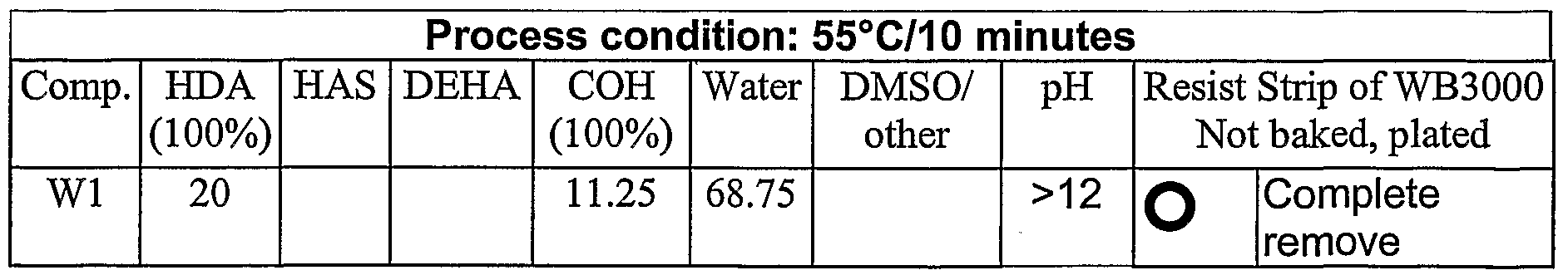


Claims


Priority Applications (5)
| Application Number | Priority Date | Filing Date | Title |
|---|---|---|---|
| EP05821234A EP1810323B1 (en) | 2004-10-29 | 2005-10-28 | Compositions and processes for photoresist stripping and residue removal in wafer level packaging |
| JP2007539278A JP5456973B2 (en) | 2004-10-29 | 2005-10-28 | Compositions and methods for photoresist stripping and residue removal in wafer level packaging |
| KR1020127033331A KR101435736B1 (en) | 2004-10-29 | 2005-10-28 | Compositions and processes for photoresist stripping and residue removal in wafer level packaging |
| CN200580045567XA CN101116178B (en) | 2004-10-29 | 2005-10-28 | Compositions and processes for photoresist stripping and residue removal in wafer level packaging |
| DE602005018248T DE602005018248D1 (en) | 2004-10-29 | 2005-10-28 | COMPOSITIONS AND METHODS FOR PHOTOOLAC RESOLUTION AND RESIDUE REMOVAL IN ABSORPTION AT WAFBERBENE |
Applications Claiming Priority (2)
| Application Number | Priority Date | Filing Date | Title |
|---|---|---|---|
| US62319004P | 2004-10-29 | 2004-10-29 | |
| US60/623,190 | 2004-10-29 |
Publications (1)
| Publication Number | Publication Date |
|---|---|
| WO2006050323A1 true WO2006050323A1 (en) | 2006-05-11 |
Family
ID=35735160
Family Applications (1)
| Application Number | Title | Priority Date | Filing Date |
|---|---|---|---|
| PCT/US2005/039381 WO2006050323A1 (en) | 2004-10-29 | 2005-10-28 | Compositions and processes for photoresist stripping and residue removal in wafer level packaging |
Country Status (8)
| Country | Link |
|---|---|
| US (1) | US20060094613A1 (en) |
| EP (1) | EP1810323B1 (en) |
| JP (2) | JP5456973B2 (en) |
| KR (2) | KR20070072622A (en) |
| CN (1) | CN101116178B (en) |
| DE (1) | DE602005018248D1 (en) |
| TW (1) | TWI469220B (en) |
| WO (1) | WO2006050323A1 (en) |
Cited By (1)
| Publication number | Priority date | Publication date | Assignee | Title |
|---|---|---|---|---|
| EP1626438A3 (en) * | 2004-08-13 | 2007-07-04 | Mitsubishi Gas Chemical Company, Inc. | Anisotropic etching agent composition used for manufacturing of micro-structures of silicon and etching method |
Families Citing this family (42)
| Publication number | Priority date | Publication date | Assignee | Title |
|---|---|---|---|---|
| US20060154186A1 (en) * | 2005-01-07 | 2006-07-13 | Advanced Technology Materials, Inc. | Composition useful for removal of post-etch photoresist and bottom anti-reflection coatings |
| US9329486B2 (en) | 2005-10-28 | 2016-05-03 | Dynaloy, Llc | Dynamic multi-purpose composition for the removal of photoresists and method for its use |
| US7632796B2 (en) * | 2005-10-28 | 2009-12-15 | Dynaloy, Llc | Dynamic multi-purpose composition for the removal of photoresists and method for its use |
| US8263539B2 (en) | 2005-10-28 | 2012-09-11 | Dynaloy, Llc | Dynamic multi-purpose composition for the removal of photoresists and methods for its use |
| US8759268B2 (en) * | 2006-08-24 | 2014-06-24 | Daikin Industries, Ltd. | Solution for removing residue after semiconductor dry process and method of removing the residue using the same |
| US8586269B2 (en) * | 2007-03-22 | 2013-11-19 | Globalfoundries Inc. | Method for forming a high resolution resist pattern on a semiconductor wafer |
| JP5428859B2 (en) * | 2007-08-08 | 2014-02-26 | 荒川化学工業株式会社 | Cleaning composition for removing lead-free solder flux and method for removing lead-free solder flux |
| KR101488265B1 (en) * | 2007-09-28 | 2015-02-02 | 삼성디스플레이 주식회사 | Composition for stripping and stripping method |
| US20110117751A1 (en) * | 2008-03-07 | 2011-05-19 | Advanced Technology Materials, Inc. | Non-selective oxide etch wet clean composition and method of use |
| US8357646B2 (en) | 2008-03-07 | 2013-01-22 | Air Products And Chemicals, Inc. | Stripper for dry film removal |
| TWI450052B (en) * | 2008-06-24 | 2014-08-21 | Dynaloy Llc | Stripper solutions effective for back-end-of-line operations |
| EP2376422A4 (en) * | 2008-12-18 | 2012-12-12 | Invista Tech Sarl | Cyclohexane oxidation process byproduct stream derivatives and methods for using the same |
| EP2427803B1 (en) | 2009-05-07 | 2017-12-13 | Basf Se | Methods for manufacturing electrical devices using resist stripping compositions |
| TWI405317B (en) * | 2010-03-04 | 2013-08-11 | Unimicron Technology Corp | Package substrate and fabrication method thereof |
| TWI539493B (en) | 2010-03-08 | 2016-06-21 | 黛納羅伊有限責任公司 | Methods and compositions for doping silicon substrates with molecular monolayers |
| US8058221B2 (en) * | 2010-04-06 | 2011-11-15 | Samsung Electronics Co., Ltd. | Composition for removing a photoresist and method of manufacturing semiconductor device using the composition |
| CN101838111B (en) * | 2010-05-20 | 2012-06-27 | 合肥茂丰电子科技有限公司 | Glass substrate etching solution and preparation method thereof |
| US9158202B2 (en) | 2012-11-21 | 2015-10-13 | Dynaloy, Llc | Process and composition for removing substances from substrates |
| US9543147B2 (en) | 2013-03-12 | 2017-01-10 | Taiwan Semiconductor Manufacturing Company, Ltd. | Photoresist and method of manufacture |
| US9502231B2 (en) | 2013-03-12 | 2016-11-22 | Taiwan Semiconductor Manufacturing Company, Ltd. | Photoresist layer and method |
| US9245751B2 (en) | 2013-03-12 | 2016-01-26 | Taiwan Semiconductor Manufacturing Company, Ltd. | Anti-reflective layer and method |
| US9256128B2 (en) | 2013-03-12 | 2016-02-09 | Taiwan Semiconductor Manufacturing Company, Ltd. | Method for manufacturing semiconductor device |
| EP2985783A4 (en) * | 2013-04-10 | 2016-05-11 | Wako Pure Chem Ind Ltd | Cleaning agent for metal wiring substrate, and method for cleaning semiconductor substrate |
| KR101420571B1 (en) * | 2013-07-05 | 2014-07-16 | 주식회사 동진쎄미켐 | Remover composition for dryfilm resist and removing method using the same |
| MY177101A (en) * | 2013-08-31 | 2020-09-07 | Hoya Corp | Method for manufacturing glass substrate for magnetic disk, and method for manufacturing magnetic disk |
| US20150104952A1 (en) * | 2013-10-11 | 2015-04-16 | Ekc Technology, Inc. | Method and composition for selectively removing metal hardmask and other residues from semiconductor device substrates comprising low-k dielectric material and copper |
| JP5977727B2 (en) * | 2013-11-13 | 2016-08-24 | 東京エレクトロン株式会社 | Substrate cleaning method, substrate cleaning system, and storage medium |
| KR20200034830A (en) | 2013-12-06 | 2020-03-31 | 후지필름 일렉트로닉 머티리얼스 유.에스.에이., 아이엔씨. | Cleaning formulation for removing residues on surfaces |
| US9401336B2 (en) | 2014-11-04 | 2016-07-26 | International Business Machines Corporation | Dual layer stack for contact formation |
| KR102637508B1 (en) * | 2015-08-03 | 2024-02-15 | 후지필름 일렉트로닉 머티리얼스 유.에스.에이., 아이엔씨. | cleaning composition |
| KR20170072701A (en) * | 2015-12-17 | 2017-06-27 | 동우 화인켐 주식회사 | Color resist stripper composition |
| KR101966674B1 (en) * | 2016-01-05 | 2019-04-09 | 후지필름 가부시키가이샤 | Process liquid, substrate cleaning method, and semiconductor device manufacturing method |
| US10073352B2 (en) * | 2016-04-12 | 2018-09-11 | Versum Materials Us, Llc | Aqueous solution and process for removing substances from substrates |
| TWI745420B (en) * | 2017-08-25 | 2021-11-11 | 聯華電子股份有限公司 | Semiconductor structure |
| CN111448520B (en) * | 2017-12-08 | 2023-11-17 | 汉高股份有限及两合公司 | Photoresist stripper composition |
| US11353794B2 (en) * | 2017-12-22 | 2022-06-07 | Versum Materials Us, Llc | Photoresist stripper |
| JP6862027B2 (en) * | 2018-01-08 | 2021-04-21 | エムティーアイ カンパニー,リミテッドMti Co.,Ltd. | Protective coating agent composition for wafer processing, and protective coating agent containing it |
| IL301529A (en) | 2018-03-28 | 2023-05-01 | Fujifilm Electronic Mat Usa Inc | Cleaning compositions |
| US11460778B2 (en) * | 2018-04-12 | 2022-10-04 | Versum Materials Us, Llc | Photoresist stripper |
| US10636696B1 (en) | 2019-01-18 | 2020-04-28 | Applied Materials, Inc. | Methods for forming vias in polymer layers |
| JP2020155721A (en) * | 2019-03-22 | 2020-09-24 | 株式会社Screenホールディングス | Substrate treatment method |
| KR20220058069A (en) * | 2020-10-30 | 2022-05-09 | 주식회사 이엔에프테크놀로지 | Composition for cleaning residue after etching or ashing from semiconductor substrate and cleaning method using same |
Citations (5)
| Publication number | Priority date | Publication date | Assignee | Title |
|---|---|---|---|---|
| EP0801422A2 (en) * | 1996-04-12 | 1997-10-15 | Mitsubishi Gas Chemical Company, Inc. | Removing agent composition for a photoresist and process for producing a semiconductor integrated circuit |
| US6546939B1 (en) * | 1990-11-05 | 2003-04-15 | Ekc Technology, Inc. | Post clean treatment |
| US20040067860A1 (en) * | 1990-11-05 | 2004-04-08 | Lee Wai Mun | Cleaning compositions and methods of use thereof |
| US20040234904A1 (en) * | 2003-05-23 | 2004-11-25 | Rieker Jennifer M. | Compositions suitable for removing photoresist, photoresist byproducts and etching residue, and use thereof |
| WO2005043250A2 (en) * | 2003-10-22 | 2005-05-12 | Ekc Technology, Inc. | Process for the use of bis-choline and tris-choline in the cleaning of quartz-coated polysilicon and other materials |
Family Cites Families (12)
| Publication number | Priority date | Publication date | Assignee | Title |
|---|---|---|---|---|
| US5279771A (en) * | 1990-11-05 | 1994-01-18 | Ekc Technology, Inc. | Stripping compositions comprising hydroxylamine and alkanolamine |
| EP0578507B1 (en) * | 1992-07-09 | 2005-09-28 | Ekc Technology, Inc. | Cleaning solutions including nucleophilic amine compound having reduction and oxidation potentials |
| KR970007328B1 (en) * | 1992-07-09 | 1997-05-07 | 이이케이시이 테크놀로지 인코포레이팃드 | Cleaning agent containing nucleophilic amine compound provided with reduction and oxidation potential |
| US6245155B1 (en) * | 1996-09-06 | 2001-06-12 | Arch Specialty Chemicals, Inc. | Method for removing photoresist and plasma etch residues |
| US6417112B1 (en) * | 1998-07-06 | 2002-07-09 | Ekc Technology, Inc. | Post etch cleaning composition and process for dual damascene system |
| US6348239B1 (en) * | 2000-04-28 | 2002-02-19 | Simon Fraser University | Method for depositing metal and metal oxide films and patterned films |
| US6440326B1 (en) * | 1998-08-13 | 2002-08-27 | Mitsubishi Gas Chemical Company, Inc. | Photoresist removing composition |
| KR100520181B1 (en) * | 1999-10-11 | 2005-10-10 | 주식회사 하이닉스반도체 | Novel photoresist monomer, polymer thereof and photoresist composition containing it |
| US7543592B2 (en) * | 2001-12-04 | 2009-06-09 | Ekc Technology, Inc. | Compositions and processes for photoresist stripping and residue removal in wafer level packaging |
| JP4267359B2 (en) * | 2002-04-26 | 2009-05-27 | 花王株式会社 | Resist stripper composition |
| KR100539225B1 (en) * | 2002-06-20 | 2005-12-27 | 삼성전자주식회사 | Negative resist composition comprising hydroxy-substituted base polymer and Si-containing crosslinker having epoxy ring and patterning method for semiconductor device using the same |
| JP2004302271A (en) * | 2003-03-31 | 2004-10-28 | Nippon Zeon Co Ltd | Stripping liquid for resist and stripping method |
-
2005
- 2005-05-02 US US11/119,559 patent/US20060094613A1/en not_active Abandoned
- 2005-10-28 EP EP05821234A patent/EP1810323B1/en not_active Expired - Fee Related
- 2005-10-28 KR KR1020077011970A patent/KR20070072622A/en not_active Application Discontinuation
- 2005-10-28 DE DE602005018248T patent/DE602005018248D1/en active Active
- 2005-10-28 KR KR1020127033331A patent/KR101435736B1/en active IP Right Grant
- 2005-10-28 JP JP2007539278A patent/JP5456973B2/en active Active
- 2005-10-28 WO PCT/US2005/039381 patent/WO2006050323A1/en active Application Filing
- 2005-10-28 TW TW94137902A patent/TWI469220B/en active
- 2005-10-28 CN CN200580045567XA patent/CN101116178B/en not_active Expired - Fee Related
-
2012
- 2012-02-24 JP JP2012039300A patent/JP5540031B2/en active Active
Patent Citations (5)
| Publication number | Priority date | Publication date | Assignee | Title |
|---|---|---|---|---|
| US6546939B1 (en) * | 1990-11-05 | 2003-04-15 | Ekc Technology, Inc. | Post clean treatment |
| US20040067860A1 (en) * | 1990-11-05 | 2004-04-08 | Lee Wai Mun | Cleaning compositions and methods of use thereof |
| EP0801422A2 (en) * | 1996-04-12 | 1997-10-15 | Mitsubishi Gas Chemical Company, Inc. | Removing agent composition for a photoresist and process for producing a semiconductor integrated circuit |
| US20040234904A1 (en) * | 2003-05-23 | 2004-11-25 | Rieker Jennifer M. | Compositions suitable for removing photoresist, photoresist byproducts and etching residue, and use thereof |
| WO2005043250A2 (en) * | 2003-10-22 | 2005-05-12 | Ekc Technology, Inc. | Process for the use of bis-choline and tris-choline in the cleaning of quartz-coated polysilicon and other materials |
Cited By (1)
| Publication number | Priority date | Publication date | Assignee | Title |
|---|---|---|---|---|
| EP1626438A3 (en) * | 2004-08-13 | 2007-07-04 | Mitsubishi Gas Chemical Company, Inc. | Anisotropic etching agent composition used for manufacturing of micro-structures of silicon and etching method |
Also Published As
| Publication number | Publication date |
|---|---|
| EP1810323B1 (en) | 2009-12-09 |
| JP5540031B2 (en) | 2014-07-02 |
| DE602005018248D1 (en) | 2010-01-21 |
| US20060094613A1 (en) | 2006-05-04 |
| TW200641561A (en) | 2006-12-01 |
| EP1810323A1 (en) | 2007-07-25 |
| JP5456973B2 (en) | 2014-04-02 |
| KR20130014610A (en) | 2013-02-07 |
| TWI469220B (en) | 2015-01-11 |
| JP2008519295A (en) | 2008-06-05 |
| CN101116178A (en) | 2008-01-30 |
| KR20070072622A (en) | 2007-07-04 |
| JP2012142588A (en) | 2012-07-26 |
| KR101435736B1 (en) | 2014-08-28 |
| CN101116178B (en) | 2011-06-15 |
Similar Documents
| Publication | Publication Date | Title |
|---|---|---|
| US7543592B2 (en) | Compositions and processes for photoresist stripping and residue removal in wafer level packaging | |
| EP1810323B1 (en) | Compositions and processes for photoresist stripping and residue removal in wafer level packaging | |
| US7579308B2 (en) | Compositions and processes for photoresist stripping and residue removal in wafer level packaging | |
| EP1470207B1 (en) | Aqueous stripping and cleaning composition | |
| US20060003910A1 (en) | Composition and method comprising same for removing residue from a substrate | |
| US20060110690A1 (en) | Treating liquid for photoresist removal, and method for treating substrate | |
| EP2206140A2 (en) | Compounds for photoresist stripping | |
| JP2002523546A (en) | Non-corrosive stripping and cleaning compositions | |
| JP2003098691A (en) | Resist removing composition and method for removing resist using the same | |
| KR100363271B1 (en) | Photoresist remover composition | |
| JP2004533010A (en) | Resist remover composition | |
| JP3742624B2 (en) | Photoresist remover composition containing ammonium fluoride | |
| KR100862988B1 (en) | Photoresist remover composition | |
| KR100742119B1 (en) | Photoresist remover composition | |
| KR100378551B1 (en) | Resist remover composition | |
| KR20020019813A (en) | Photoresist remover composition comprising ammonium fluoride |
Legal Events
| Date | Code | Title | Description |
|---|---|---|---|
| AK | Designated states |
Kind code of ref document: A1 Designated state(s): AE AG AL AM AT AU AZ BA BB BG BR BW BY BZ CA CH CN CO CR CU CZ DE DK DM DZ EC EE EG ES FI GB GD GE GH GM HR HU ID IL IN IS JP KE KG KM KN KP KR KZ LC LK LR LS LT LU LV LY MA MD MG MK MN MW MX MZ NA NG NI NO NZ OM PG PH PL PT RO RU SC SD SE SG SK SL SM SY TJ TM TN TR TT TZ UA UG US UZ VC VN YU ZA ZM ZW |
|
| AL | Designated countries for regional patents |
Kind code of ref document: A1 Designated state(s): BW GH GM KE LS MW MZ NA SD SL SZ TZ UG ZM ZW AM AZ BY KG KZ MD RU TJ TM AT BE BG CH CY CZ DE DK EE ES FI FR GB GR HU IE IS IT LT LU LV MC NL PL PT RO SE SI SK TR BF BJ CF CG CI CM GA GN GQ GW ML MR NE SN TD TG |
|
| DPE2 | Request for preliminary examination filed before expiration of 19th month from priority date (pct application filed from 20040101) | ||
| 121 | Ep: the epo has been informed by wipo that ep was designated in this application | ||
| WWE | Wipo information: entry into national phase |
Ref document number: 2007539278 Country of ref document: JP |
|
| NENP | Non-entry into the national phase |
Ref country code: DE |
|
| WWE | Wipo information: entry into national phase |
Ref document number: 2005821234 Country of ref document: EP |
|
| WWE | Wipo information: entry into national phase |
Ref document number: 1020077011970 Country of ref document: KR |
|
| WWE | Wipo information: entry into national phase |
Ref document number: 200580045567.X Country of ref document: CN |
|
| WWP | Wipo information: published in national office |
Ref document number: 2005821234 Country of ref document: EP |
|
| WWE | Wipo information: entry into national phase |
Ref document number: 1020127033331 Country of ref document: KR |