EP0798876B1 - Schaltungsanordnung zur Leitungsanpassung und Echounterdrückung - Google Patents
Schaltungsanordnung zur Leitungsanpassung und Echounterdrückung Download PDFInfo
- Publication number
- EP0798876B1 EP0798876B1 EP97103944A EP97103944A EP0798876B1 EP 0798876 B1 EP0798876 B1 EP 0798876B1 EP 97103944 A EP97103944 A EP 97103944A EP 97103944 A EP97103944 A EP 97103944A EP 0798876 B1 EP0798876 B1 EP 0798876B1
- Authority
- EP
- European Patent Office
- Prior art keywords
- digital
- analog
- analogue
- signal
- filter
- Prior art date
- Legal status (The legal status is an assumption and is not a legal conclusion. Google has not performed a legal analysis and makes no representation as to the accuracy of the status listed.)
- Expired - Lifetime
Links
Images
Classifications
-
- H—ELECTRICITY
- H04—ELECTRIC COMMUNICATION TECHNIQUE
- H04B—TRANSMISSION
- H04B7/00—Radio transmission systems, i.e. using radiation field
- H04B7/015—Reducing echo effects
-
- H—ELECTRICITY
- H04—ELECTRIC COMMUNICATION TECHNIQUE
- H04B—TRANSMISSION
- H04B3/00—Line transmission systems
- H04B3/02—Details
- H04B3/20—Reducing echo effects or singing; Opening or closing transmitting path; Conditioning for transmission in one direction or the other
- H04B3/23—Reducing echo effects or singing; Opening or closing transmitting path; Conditioning for transmission in one direction or the other using a replica of transmitted signal in the time domain, e.g. echo cancellers
Definitions
- the invention relates to a circuit arrangement for line adaptation and echo cancellation with a balance filter which is driven by transmit signals and whose output signals are combined with a receive signal by means of a subtractor, with an impedance matching filter which is driven by the receive signals and whose output signals are linked to the transmit signal by means of an adder with an analog-to-digital converter for converting analog reception signals into digital reception signals and with a digital-to-analog converter for converting digital transmission signals into analog transmission signals.
- Such a circuit arrangement is described, for example, by D. Vogel, E. Schmid, J. Reisinger, L. Lerach, "A Signal-Processing Codec Filter for PCM Applications", Siemens Research and Development Reports 15 (1986), No. 5, Berlin, Pages 253 to 258 known.
- an analog-to-digital converter located in the reception path as well as a digital-to-analog converter located in the transmission path are provided.
- an impedance matching filter (Z filter) and a balance filter (B filter) are used, wherein the impedance matching filter picks up digital received signals at the output of the analog-to-digital converter, filters them.
- the output signal of the impedance matched filter is coupled to the transmission signal to the digital-to-analogue converter.
- the balance filter is also executed digitally and is accordingly controlled by the digital transmission signal.
- the output of the balance filter is linked to the digital received signal.
- US Pat. No. 4,796,296 also discloses a coding and decoding device which contains two balance filters, wherein a first digital balance filter processes the digital transmission signal and a second analog balance filter supplies an analog transmission signal.
- a first digital balance filter processes the digital transmission signal
- a second analog balance filter supplies an analog transmission signal.
- Input circuit arrangements are used in particular in electronic two-wire four-wire converters, but in which, depending on the line length, echo terms may arise, which may be many times greater than the received useful signal. These echo terms should be filtered out by the balance filter. For this purpose, the echo path is reproduced by the balance filter, wherein the echo terms are removed by the subsequent subtraction output signals from the received signal. However, only the extinction of linear terms can be achieved. If the digital-to-analog converter and / or the analog-to-digital converter produce harmonics due to their nonlinearities, they arrive unfiltered in the receive path and thus reduce the achievable signal-to-noise ratio.
- the object of the invention is to provide a circuit arrangement of the type mentioned, in which these disadvantages do not occur.
- the Impedanzanpezefilter is executed digitally, so that this can be programmed in a simple way and even complex filter terms can be considered without much effort.
- the balance filter is realized with reasonable effort in analog technology, whereby not only linear echo terms, but also harmonic components, in particular of the digital-to-analog converter, can be filtered out.
- the non-linearities of the analog-to-digital converter no longer play a role, since the levels of the echo signal are already strongly attenuated before the analog-to-digital converter by the balance filter. All this is accomplished by placing the balance filter on the analog side and the impedance matching filter on the digital side.
- analog reception signals are applied to the impedance matching filter with the interposition of a further analog-to-digital converter.
- influences of the balance filter are eliminated on the impedance matching filter due to the further analog-to-digital converter and justified by this additional signal path.
- the requirements for the analog signal processing balance filter are reduced by a digital signals processing, further balance filter, so that the cost of the analog balance filter is greatly reduced without major loss of transmission quality.
- a desired balance filter can be divided so that the analog sub-filter achieves the highest possible base echo attenuation with relatively simple means, while the remaining echo damping, which would require a high additional effort, for example, is realized in a simple manner with digital means. Consequently, an optimal cost-benefit ratio is achieved by the additional balance filter and a corresponding design of the two balance filters.
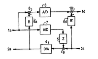
- an analog-to-digital converter 3 for converting an analog received signal 1a into a digital received signal 1d and a digital-to-analog converter 4 for converting a digital transmission signal 2d is provided in an analog transmission signal 2a.
- An analog balance filter 6a with a suitable for echo cancellation transmission behavior is the input side connected to the output of the digital-to-analog converter 4 and is therefore by the analog transmission signal 2a activated.
- the output of the analog balance filter 6a is connected to the inverting input of an analog subtracter 8, via whose non-inverting input and whose output the analog receive signal 1a is fed to the analog-to-digital converter 3. Disturbing echo signals are consequently filtered out by the analog balance filter 6a and subtracted from the analog received signal 1a by means of the analog subtracter 8.
- an impedance matching filter 5 is provided, which is driven according to an embodiment of the invention with the interposition of another analog-to-digital converter 7 by the analog received signal 1a.
- the output of the impedance matching filter 5 is connected to an input of a digital adder 9, via whose other input and whose output the digital transmission signal 2d is fed to the input of the digital-to-analog converter 4.
- a digital, further balance filter 6d is connected between digital transmission path and digital reception path.
- the digital transmission signal 2d is applied to the input of the digital balance filter 6d whose output is connected to the inverting input of a digital subtractor 10. Its non-inverting input is in turn connected to the output of the analog-to-digital converter 3 and its output carries the digital received signal 1d.
- the digital balance filter 6d supplements the analog balance filter 6a in such a way that the analog balance filter 6a already offers good precompensation, in particular with regard to the extinction of nonlinear terms, and the digital balance filter 6d suppresses remaining echoes with little outlay in terms of circuitry, the precompensation being advantageous the requirements for the analog-to-digital converter 3 and the digital-to-analog converter 4 are reduced.
- the design of the balance filters 6a and 6d and the impedance matching filter 5 as well as the choice of corresponding analog-to-digital converters 3 and 7 and the digital-to-analog converter 4 depends on the individual case and can therefore vary within a wide range.
- the converters 3, 7, 4 can work according to any Umsetzertexien and any additional resources such as upstream and downstream filters, sample and hold facilities, etc. include.
- the adder can also be a subtractor and instead of the subtractor and adder can be used in a corresponding signal phase position.
- the circuit arrangement shown in the embodiment is preferably preceded by a not shown in detail in the drawing two-wire four-wire converter, which in turn is connected, for example, to a two-wire telephone line.
Landscapes
- Engineering & Computer Science (AREA)
- Computer Networks & Wireless Communication (AREA)
- Signal Processing (AREA)
- Cable Transmission Systems, Equalization Of Radio And Reduction Of Echo (AREA)
Applications Claiming Priority (2)
| Application Number | Priority Date | Filing Date | Title |
|---|---|---|---|
| DE19611941 | 1996-03-26 | ||
| DE19611941A DE19611941C1 (de) | 1996-03-26 | 1996-03-26 | Schaltungsanordnung zur Leitungsanpassung und Echounterdrückung |
Publications (3)
| Publication Number | Publication Date |
|---|---|
| EP0798876A2 EP0798876A2 (de) | 1997-10-01 |
| EP0798876A3 EP0798876A3 (de) | 2003-06-25 |
| EP0798876B1 true EP0798876B1 (de) | 2006-05-31 |
Family
ID=7789483
Family Applications (1)
| Application Number | Title | Priority Date | Filing Date |
|---|---|---|---|
| EP97103944A Expired - Lifetime EP0798876B1 (de) | 1996-03-26 | 1997-03-10 | Schaltungsanordnung zur Leitungsanpassung und Echounterdrückung |
Country Status (5)
| Country | Link |
|---|---|
| US (1) | US5969567A (zh) |
| EP (1) | EP0798876B1 (zh) |
| CN (1) | CN1110912C (zh) |
| DE (2) | DE19611941C1 (zh) |
| TW (1) | TW355889B (zh) |
Families Citing this family (3)
| Publication number | Priority date | Publication date | Assignee | Title |
|---|---|---|---|---|
| JP3630369B2 (ja) * | 1999-02-05 | 2005-03-16 | インフィネオン テクノロジース アクチエンゲゼルシャフト | アナログエコーフィルタ |
| DE19933485B4 (de) * | 1999-07-16 | 2004-05-13 | Infineon Technologies Ag | Leitungsabschlußeinrichtung für eine Telefon-Teilnehmeranschlußleitung |
| DE10112559B4 (de) * | 2001-03-15 | 2005-04-28 | Infineon Technologies Ag | xDSL-Modem mit digitaler Splitter-Vorrichtung |
Family Cites Families (5)
| Publication number | Priority date | Publication date | Assignee | Title |
|---|---|---|---|---|
| GB1583634A (en) * | 1977-03-02 | 1981-01-28 | Int Standard Electric Corp | Subscriber line/trunk circuit |
| JPS5829012B2 (ja) * | 1978-05-16 | 1983-06-20 | ケイディディ株式会社 | エコ−制御方式 |
| DE3586696T2 (de) * | 1984-05-30 | 1993-04-01 | Hitachi Ltd | Pcm-coder/decoder mit zweidraht/vierdrahtumwandlung. |
| SE463589B (sv) * | 1989-04-27 | 1990-12-10 | Ericsson Telefon Ab L M | Foerfarande foer att undvika felaktig ekoeliminering och/eller utjaemning till foeljd av olinjaeriteter i en d/a-omvandlare och/eller en a/d-omvandlare i en telekommunikationsanlaeggning, samt anordning foer utoevande av foerfarandet i samband med d/a-omvandling och anordning foer utoevande av foerfarandet i samband med a/d-omvandling |
| US5307405A (en) * | 1992-09-25 | 1994-04-26 | Qualcomm Incorporated | Network echo canceller |
-
1996
- 1996-03-26 DE DE19611941A patent/DE19611941C1/de not_active Expired - Fee Related
-
1997
- 1997-03-10 EP EP97103944A patent/EP0798876B1/de not_active Expired - Lifetime
- 1997-03-10 DE DE59712661T patent/DE59712661D1/de not_active Expired - Lifetime
- 1997-03-25 TW TW086103771A patent/TW355889B/zh not_active IP Right Cessation
- 1997-03-26 CN CN97104912A patent/CN1110912C/zh not_active Expired - Fee Related
- 1997-03-26 US US08/824,442 patent/US5969567A/en not_active Expired - Lifetime
Also Published As
| Publication number | Publication date |
|---|---|
| EP0798876A2 (de) | 1997-10-01 |
| US5969567A (en) | 1999-10-19 |
| CN1168587A (zh) | 1997-12-24 |
| DE59712661D1 (de) | 2006-07-06 |
| TW355889B (en) | 1999-04-11 |
| EP0798876A3 (de) | 2003-06-25 |
| CN1110912C (zh) | 2003-06-04 |
| DE19611941C1 (de) | 1997-12-11 |
Similar Documents
| Publication | Publication Date | Title |
|---|---|---|
| DE3021012A1 (de) | Verallgemeinertes interpolativers verfahren zur digital-analog-umsetzung von pcm signalen | |
| DE2713478A1 (de) | Logarithmischer echokompensator | |
| DE2734941A1 (de) | Echoausloescheinrichtung | |
| DE3044582C2 (de) | Digitaler Verstärker, insbesondere zur Verwendung in einer digitalen Fernsprech-Teilnehmerschaltung | |
| EP0448753B1 (de) | Zweidraht-Vierdraht-Umsetzer | |
| EP0798876B1 (de) | Schaltungsanordnung zur Leitungsanpassung und Echounterdrückung | |
| EP0448754B1 (de) | Zweidraht-Vierdraht-Umsetzer | |
| EP1149478B1 (de) | Analoges echofilter | |
| DE2911866C3 (de) | Anordnung mit einer Gabelschaltung für den Zweidraht-Vierdraht-Übergang in PCM-Zeitmultiplexsystemen | |
| DE4227327A1 (de) | Teilbandechokompensator mit Teilbandcodiereinrichtung | |
| CH652877A5 (de) | Digital/analog-wandler. | |
| EP0019194B1 (de) | Digital-Fernmeldesystem mit mindestens einem Vierdrahtleitungsabschnitt | |
| DE2455584B2 (de) | Freisprecheinrichtung | |
| EP0855806B1 (de) | Echosperre für ein Spracheingabe Dialogsystem | |
| DE4221397C2 (de) | Integrierte PCM-Codec-Schaltung für ein Vermittlungssystem | |
| EP0953234B1 (de) | Schaltungsanordnung zur zweidraht-vierdraht-umsetzung | |
| DE3212056A1 (de) | Verfahren und schaltungsanordnung zur durchfuehrung des verfahrens zur adaptiven echoloeschung in endgeraeten fuer duplex-datenuebertragung ueber zweidrahtleitungen | |
| EP0467367B1 (de) | Teilnehmeranschlussschaltung zum Anschluss einer Teilnehmeranschlussleitung für die Übertragung von analogen Teilnehmersignalen an die Vermittlungsstelle einer digitalen Zeitmultiplex-Fernsprechvermittlungsstelle | |
| EP0543274B1 (de) | Verfahren und Anordnung zur Steuerung eines Restecho-Begrenzers | |
| EP1325620B1 (de) | Datenubertragung uber eine funkschnittstelle | |
| EP0642229B1 (de) | Schaltungsanordnung zur Erzeugung einer variablen Leitungsabschlussimpedanz | |
| DE4410058C1 (de) | Schaltungsanordnung zur Gebührenimpulsfilterung | |
| EP0231854A1 (de) | Echokompensator | |
| EP0270189A2 (de) | Konferenzschaltung für ein digitales Nachrichtensystem | |
| DE432495C (de) | Signalsystem fuer gleichzeitiges Telegraphieren und Telephonieren ueber mit Induktionsspulen ausgeruestete Leitungen |
Legal Events
| Date | Code | Title | Description |
|---|---|---|---|
| PUAI | Public reference made under article 153(3) epc to a published international application that has entered the european phase |
Free format text: ORIGINAL CODE: 0009012 |
|
| AK | Designated contracting states |
Kind code of ref document: A2 Designated state(s): DE FR GB IT |
|
| RAP1 | Party data changed (applicant data changed or rights of an application transferred) |
Owner name: INFINEON TECHNOLOGIES AG |
|
| PUAL | Search report despatched |
Free format text: ORIGINAL CODE: 0009013 |
|
| AK | Designated contracting states |
Designated state(s): DE FR GB IT |
|
| RIC1 | Information provided on ipc code assigned before grant |
Ipc: 7H 04B 3/23 B Ipc: 7H 04B 3/20 A |
|
| 17P | Request for examination filed |
Effective date: 20030805 |
|
| 17Q | First examination report despatched |
Effective date: 20040803 |
|
| GRAP | Despatch of communication of intention to grant a patent |
Free format text: ORIGINAL CODE: EPIDOSNIGR1 |
|
| GRAS | Grant fee paid |
Free format text: ORIGINAL CODE: EPIDOSNIGR3 |
|
| GRAA | (expected) grant |
Free format text: ORIGINAL CODE: 0009210 |
|
| AK | Designated contracting states |
Kind code of ref document: B1 Designated state(s): DE FR GB IT |
|
| PG25 | Lapsed in a contracting state [announced via postgrant information from national office to epo] |
Ref country code: IT Free format text: LAPSE BECAUSE OF FAILURE TO SUBMIT A TRANSLATION OF THE DESCRIPTION OR TO PAY THE FEE WITHIN THE PRE;WARNING: LAPSES OF ITALIAN PATENTS WITH EFFECTIVE DATE BEFORE 2007 MAY HAVE OCCURRED AT ANY TIME BEFORE 2007. THE CORRECT EFFECTIVE DATE MAY BE DIFFERENT FROM THE ONE RECORDED.SCRIBED TIME-LIMIT Effective date: 20060531 |
|
| REG | Reference to a national code |
Ref country code: GB Ref legal event code: FG4D Free format text: NOT ENGLISH |
|
| REF | Corresponds to: |
Ref document number: 59712661 Country of ref document: DE Date of ref document: 20060706 Kind code of ref document: P |
|
| GBT | Gb: translation of ep patent filed (gb section 77(6)(a)/1977) |
Effective date: 20060920 |
|
| ET | Fr: translation filed | ||
| PLBE | No opposition filed within time limit |
Free format text: ORIGINAL CODE: 0009261 |
|
| STAA | Information on the status of an ep patent application or granted ep patent |
Free format text: STATUS: NO OPPOSITION FILED WITHIN TIME LIMIT |
|
| 26N | No opposition filed |
Effective date: 20070301 |
|
| REG | Reference to a national code |
Ref country code: FR Ref legal event code: TP |
|
| REG | Reference to a national code |
Ref country code: DE Ref legal event code: R081 Ref document number: 59712661 Country of ref document: DE Owner name: LANTIQ DEUTSCHLAND GMBH, DE Free format text: FORMER OWNER: INFINEON TECHNOLOGIES AG, 81669 MUENCHEN, DE Effective date: 20110325 |
|
| REG | Reference to a national code |
Ref country code: GB Ref legal event code: 732E Free format text: REGISTERED BETWEEN 20110602 AND 20110608 |
|
| REG | Reference to a national code |
Ref country code: GB Ref legal event code: 732E Free format text: REGISTERED BETWEEN 20110609 AND 20110615 |
|
| PGFP | Annual fee paid to national office [announced via postgrant information from national office to epo] |
Ref country code: FR Payment date: 20120403 Year of fee payment: 16 |
|
| PGFP | Annual fee paid to national office [announced via postgrant information from national office to epo] |
Ref country code: DE Payment date: 20120323 Year of fee payment: 16 |
|
| PGFP | Annual fee paid to national office [announced via postgrant information from national office to epo] |
Ref country code: GB Payment date: 20120322 Year of fee payment: 16 |
|
| GBPC | Gb: european patent ceased through non-payment of renewal fee |
Effective date: 20130310 |
|
| REG | Reference to a national code |
Ref country code: FR Ref legal event code: ST Effective date: 20131129 |
|
| REG | Reference to a national code |
Ref country code: DE Ref legal event code: R119 Ref document number: 59712661 Country of ref document: DE Effective date: 20131001 |
|
| PG25 | Lapsed in a contracting state [announced via postgrant information from national office to epo] |
Ref country code: FR Free format text: LAPSE BECAUSE OF NON-PAYMENT OF DUE FEES Effective date: 20130402 Ref country code: GB Free format text: LAPSE BECAUSE OF NON-PAYMENT OF DUE FEES Effective date: 20130310 Ref country code: DE Free format text: LAPSE BECAUSE OF NON-PAYMENT OF DUE FEES Effective date: 20131001 |