EP0798876B1 - Circuit for line matching and echo suppressing - Google Patents
Circuit for line matching and echo suppressing Download PDFInfo
- Publication number
- EP0798876B1 EP0798876B1 EP97103944A EP97103944A EP0798876B1 EP 0798876 B1 EP0798876 B1 EP 0798876B1 EP 97103944 A EP97103944 A EP 97103944A EP 97103944 A EP97103944 A EP 97103944A EP 0798876 B1 EP0798876 B1 EP 0798876B1
- Authority
- EP
- European Patent Office
- Prior art keywords
- digital
- analog
- analogue
- signal
- filter
- Prior art date
- Legal status (The legal status is an assumption and is not a legal conclusion. Google has not performed a legal analysis and makes no representation as to the accuracy of the status listed.)
- Expired - Lifetime
Links
Images
Classifications
-
- H—ELECTRICITY
- H04—ELECTRIC COMMUNICATION TECHNIQUE
- H04B—TRANSMISSION
- H04B7/00—Radio transmission systems, i.e. using radiation field
- H04B7/015—Reducing echo effects
-
- H—ELECTRICITY
- H04—ELECTRIC COMMUNICATION TECHNIQUE
- H04B—TRANSMISSION
- H04B3/00—Line transmission systems
- H04B3/02—Details
- H04B3/20—Reducing echo effects or singing; Opening or closing transmitting path; Conditioning for transmission in one direction or the other
- H04B3/23—Reducing echo effects or singing; Opening or closing transmitting path; Conditioning for transmission in one direction or the other using a replica of transmitted signal in the time domain, e.g. echo cancellers
Definitions
- the invention relates to a circuit arrangement for line adaptation and echo cancellation with a balance filter which is driven by transmit signals and whose output signals are combined with a receive signal by means of a subtractor, with an impedance matching filter which is driven by the receive signals and whose output signals are linked to the transmit signal by means of an adder with an analog-to-digital converter for converting analog reception signals into digital reception signals and with a digital-to-analog converter for converting digital transmission signals into analog transmission signals.
- Such a circuit arrangement is described, for example, by D. Vogel, E. Schmid, J. Reisinger, L. Lerach, "A Signal-Processing Codec Filter for PCM Applications", Siemens Research and Development Reports 15 (1986), No. 5, Berlin, Pages 253 to 258 known.
- an analog-to-digital converter located in the reception path as well as a digital-to-analog converter located in the transmission path are provided.
- an impedance matching filter (Z filter) and a balance filter (B filter) are used, wherein the impedance matching filter picks up digital received signals at the output of the analog-to-digital converter, filters them.
- the output signal of the impedance matched filter is coupled to the transmission signal to the digital-to-analogue converter.
- the balance filter is also executed digitally and is accordingly controlled by the digital transmission signal.
- the output of the balance filter is linked to the digital received signal.
- US Pat. No. 4,796,296 also discloses a coding and decoding device which contains two balance filters, wherein a first digital balance filter processes the digital transmission signal and a second analog balance filter supplies an analog transmission signal.
- a first digital balance filter processes the digital transmission signal
- a second analog balance filter supplies an analog transmission signal.
- Input circuit arrangements are used in particular in electronic two-wire four-wire converters, but in which, depending on the line length, echo terms may arise, which may be many times greater than the received useful signal. These echo terms should be filtered out by the balance filter. For this purpose, the echo path is reproduced by the balance filter, wherein the echo terms are removed by the subsequent subtraction output signals from the received signal. However, only the extinction of linear terms can be achieved. If the digital-to-analog converter and / or the analog-to-digital converter produce harmonics due to their nonlinearities, they arrive unfiltered in the receive path and thus reduce the achievable signal-to-noise ratio.
- the object of the invention is to provide a circuit arrangement of the type mentioned, in which these disadvantages do not occur.
- the Impedanzanpezefilter is executed digitally, so that this can be programmed in a simple way and even complex filter terms can be considered without much effort.
- the balance filter is realized with reasonable effort in analog technology, whereby not only linear echo terms, but also harmonic components, in particular of the digital-to-analog converter, can be filtered out.
- the non-linearities of the analog-to-digital converter no longer play a role, since the levels of the echo signal are already strongly attenuated before the analog-to-digital converter by the balance filter. All this is accomplished by placing the balance filter on the analog side and the impedance matching filter on the digital side.
- analog reception signals are applied to the impedance matching filter with the interposition of a further analog-to-digital converter.
- influences of the balance filter are eliminated on the impedance matching filter due to the further analog-to-digital converter and justified by this additional signal path.
- the requirements for the analog signal processing balance filter are reduced by a digital signals processing, further balance filter, so that the cost of the analog balance filter is greatly reduced without major loss of transmission quality.
- a desired balance filter can be divided so that the analog sub-filter achieves the highest possible base echo attenuation with relatively simple means, while the remaining echo damping, which would require a high additional effort, for example, is realized in a simple manner with digital means. Consequently, an optimal cost-benefit ratio is achieved by the additional balance filter and a corresponding design of the two balance filters.
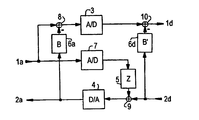
- an analog-to-digital converter 3 for converting an analog received signal 1a into a digital received signal 1d and a digital-to-analog converter 4 for converting a digital transmission signal 2d is provided in an analog transmission signal 2a.
- An analog balance filter 6a with a suitable for echo cancellation transmission behavior is the input side connected to the output of the digital-to-analog converter 4 and is therefore by the analog transmission signal 2a activated.
- the output of the analog balance filter 6a is connected to the inverting input of an analog subtracter 8, via whose non-inverting input and whose output the analog receive signal 1a is fed to the analog-to-digital converter 3. Disturbing echo signals are consequently filtered out by the analog balance filter 6a and subtracted from the analog received signal 1a by means of the analog subtracter 8.
- an impedance matching filter 5 is provided, which is driven according to an embodiment of the invention with the interposition of another analog-to-digital converter 7 by the analog received signal 1a.
- the output of the impedance matching filter 5 is connected to an input of a digital adder 9, via whose other input and whose output the digital transmission signal 2d is fed to the input of the digital-to-analog converter 4.
- a digital, further balance filter 6d is connected between digital transmission path and digital reception path.
- the digital transmission signal 2d is applied to the input of the digital balance filter 6d whose output is connected to the inverting input of a digital subtractor 10. Its non-inverting input is in turn connected to the output of the analog-to-digital converter 3 and its output carries the digital received signal 1d.
- the digital balance filter 6d supplements the analog balance filter 6a in such a way that the analog balance filter 6a already offers good precompensation, in particular with regard to the extinction of nonlinear terms, and the digital balance filter 6d suppresses remaining echoes with little outlay in terms of circuitry, the precompensation being advantageous the requirements for the analog-to-digital converter 3 and the digital-to-analog converter 4 are reduced.
- the design of the balance filters 6a and 6d and the impedance matching filter 5 as well as the choice of corresponding analog-to-digital converters 3 and 7 and the digital-to-analog converter 4 depends on the individual case and can therefore vary within a wide range.
- the converters 3, 7, 4 can work according to any Umsetzertexien and any additional resources such as upstream and downstream filters, sample and hold facilities, etc. include.
- the adder can also be a subtractor and instead of the subtractor and adder can be used in a corresponding signal phase position.
- the circuit arrangement shown in the embodiment is preferably preceded by a not shown in detail in the drawing two-wire four-wire converter, which in turn is connected, for example, to a two-wire telephone line.
Description
Die Erfindung betrifft eine Schaltungsanordnung zur Leitungsanpassung und Echounterdrückung mit einem Balancefilter, das durch Sendesignale angesteuert wird und dessen Ausgangssignale mit einem Empfangssignal mittels einer Subtrahiereinrichtung verknüpft werden, mit einem Impedanzanpaßfilter, das durch die Empfangssignale angesteuert wird und dessen Ausgangssignale mit dem Sendesignal mittels einer Addiereinrichtung verknüpft werden, mit einem Analog-Digital-Umsetzer zur Umsetzung von analogen Empfangssignalen in digitale Empfangssignale und mit einem Digital-Analog-Umsetzer zur Umsetzung von digitalen Sendesignalen in analoge Sendesignale.The invention relates to a circuit arrangement for line adaptation and echo cancellation with a balance filter which is driven by transmit signals and whose output signals are combined with a receive signal by means of a subtractor, with an impedance matching filter which is driven by the receive signals and whose output signals are linked to the transmit signal by means of an adder with an analog-to-digital converter for converting analog reception signals into digital reception signals and with a digital-to-analog converter for converting digital transmission signals into analog transmission signals.
Eine derartige Schaltungsanordnung ist beispielsweise aus D. Vogel, E. Schmid, J. Reisinger, L. Lerach, "A Signal-Processing Codec Filter for PCM Applications", Siemens Forschungs- und Entwicklungsberichte 15 (1986), Nr. 5, Berlin, Seiten 253 bis 258 bekannt. Dabei sind ein im Empfangsweg befindlicher Analog-Digital-Umsetzer sowie ein im Sendeweg befindlicher Digital-Analog-Umsetzer vorgesehen. Auf digitaler Seite werden ein Impedanzanpaßfilter (Z-Filter) und ein Balancefilter (B-Filter) verwendet, wobei das Impedanzanpaßfilter digitale Empfangssignale am Ausgang des Analog-Digital-Umsetzers abgreift, diese filtert. Mittels der Addiereinrichtung wird das Ausgangssignal des Impedanzpaßfilters mit dem Sendesignal verknüpft dem Digital-Analog-Umsetzer zuführt. Das Balancefilter ist ebenfalls digital ausgeführt und wird dementsprechend von dem digitalen Sendesignal angesteuert. Über die Subtrahiereinrichtung (oder eine weitere Addiereinrichtung) wird das Ausgangssignal des Balancefilters mit dem digitalen Empfangssignal verknüpft.Such a circuit arrangement is described, for example, by D. Vogel, E. Schmid, J. Reisinger, L. Lerach, "A Signal-Processing Codec Filter for PCM Applications", Siemens Research and Development Reports 15 (1986), No. 5, Berlin, Pages 253 to 258 known. In this case, an analog-to-digital converter located in the reception path as well as a digital-to-analog converter located in the transmission path are provided. On the digital side, an impedance matching filter (Z filter) and a balance filter (B filter) are used, wherein the impedance matching filter picks up digital received signals at the output of the analog-to-digital converter, filters them. By means of the adding device, the output signal of the impedance matched filter is coupled to the transmission signal to the digital-to-analogue converter. The balance filter is also executed digitally and is accordingly controlled by the digital transmission signal. About the subtractor (or another adder), the output of the balance filter is linked to the digital received signal.
Auch in der US Patentschrift Nr. 4,796,296 ist eine Kodier- und Dekodiereinrichtung offenbart, die zwei Balancefilter enthält, wobei ein erstes digitales Balancefilter das digitale Sendesignal verarbeitet und einem zweiten analogen Balancefilter ein analoges Sendesignal zugeführt ist. Das Problem einer steuerbaren Impedanzanpassung ist in diesem Dokument nicht adressiert.US Pat. No. 4,796,296 also discloses a coding and decoding device which contains two balance filters, wherein a first digital balance filter processes the digital transmission signal and a second analog balance filter supplies an analog transmission signal. The problem of controllable impedance matching is not addressed in this document.
Eingangs genannte Schaltungsanordnungen werden insbesondere bei elektronischen Zweidraht-Vierdraht-Umsetzern verwendet, bei denen jedoch, je nach Leitungslänge, Echoterme entstehen können, die unter Umständen um ein Vielfaches größer sind, als das empfangene Nutzsignal. Diese Echoterme sollen durch das Balancefilter herausgefiltert werden. Zu diesem Zweck wird durch das Balancefilter der Echopfad nachgebildet, wobei durch die nachfolgende Subtraktion Ausgangssignale vom Empfangssignal die Echoterme entfernt werden. Dabei kann jedoch nur die Auslöschung von linearen Termen erreicht werden. Produziert der Digital-Analog-Umsetzer und/oder der Analog-Digital-Umsetzer aufgrund ihrer Nichtlinearitäten Oberwellen, so gelangen diese ungefiltert in den Empfangspfad und reduzieren somit den erreichbaren Signal-Rausch-Abstand.Input circuit arrangements are used in particular in electronic two-wire four-wire converters, but in which, depending on the line length, echo terms may arise, which may be many times greater than the received useful signal. These echo terms should be filtered out by the balance filter. For this purpose, the echo path is reproduced by the balance filter, wherein the echo terms are removed by the subsequent subtraction output signals from the received signal. However, only the extinction of linear terms can be achieved. If the digital-to-analog converter and / or the analog-to-digital converter produce harmonics due to their nonlinearities, they arrive unfiltered in the receive path and thus reduce the achievable signal-to-noise ratio.
Aufgabe der Erfindung ist es, eine Schaltungsanordnung der eingangs genannten Art anzugeben, bei der diese Nachteile nicht auftreten.The object of the invention is to provide a circuit arrangement of the type mentioned, in which these disadvantages do not occur.
Die Aufgabe wird gelöst durch eine Schaltungsanordnung gemäß Patentanspruch 1. Ausgestaltungen und Weiterbildungen des Erfindungsgedankens sind Gegenstand von Unteransprüchen.The object is achieved by a circuit arrangement according to claim 1. refinements and developments of the inventive concept are the subject of dependent claims.
Vorteil dabei ist, daß das Impedanzanpaßfilter digital ausgeführt ist, so daß dieses auf einfache Weise programmiert werden kann und auch komplexe Filterterme ohne großen Aufwand berücksichtigt werden können. Das Balancefilter dagegen wird in analoger Technik mit vertretbarem Aufwand realisiert, wobei nicht nur lineare Echoterme, sondern auch harmonische Anteile insbesondere des Digital-Analog-Umsetzers herausgefiltert werden können. Die Nichtlinearitäten des Analog-Digital-Umsetzers spielen darüber hinaus ebenso keine Rolle mehr, da die Pegel des Echosignals bereits vor dem Analog-Digital-Umsetzer durch das Balancefilter stark gedämpft werden. Dies alles wird dadurch erreicht, daß das Balancefilter auf analoger Seite und das Impedanzanpaßfilter auf digitaler Seite angeordnet wird.The advantage here is that the Impedanzanpaßfilter is executed digitally, so that this can be programmed in a simple way and even complex filter terms can be considered without much effort. By contrast, the balance filter is realized with reasonable effort in analog technology, whereby not only linear echo terms, but also harmonic components, in particular of the digital-to-analog converter, can be filtered out. In addition, the non-linearities of the analog-to-digital converter no longer play a role, since the levels of the echo signal are already strongly attenuated before the analog-to-digital converter by the balance filter. All this is accomplished by placing the balance filter on the analog side and the impedance matching filter on the digital side.
Weiter ist vorgesehen, daß an das Impedanzanpaßfilter unter Zwischenschaltung eines weiteren Analog-Digital-Umsetzers die analogen Empfangssignale angelegt sind. Bei dieser Weiterbildung der Erfindung werden Einflüsse des Balancefilters auf das Impedanzanpaßfilter aufgrund des weiteren Analog-Digital-Umsetzers und des durch diesen begründeten zusätzlichen Signalpfads eliminiert.It is further provided that the analog reception signals are applied to the impedance matching filter with the interposition of a further analog-to-digital converter. In this embodiment of the invention influences of the balance filter are eliminated on the impedance matching filter due to the further analog-to-digital converter and justified by this additional signal path.
Schließlich werden durch ein digitale Signale verarbeitendes, weiteres Balancefilter die Anforderungen an das analoge Signale verarbeitende Balancefilter herabgesetzt, so daß der Aufwand für das analoge Balancefilter ohne größere Einbußen an Übertragungsqualität stark herabgesetzt wird. Damit kann beispielsweise ein gewünschtes Balancefilter derart aufgeteilt werden, daß das analoge Teilfilter mit relativ einfachen Mitteln eine möglichst hohe Grundechodämpfung erreicht, während die restliche Echodämpfung, die beispielsweise einen hohen zusätzlichen Aufwand erfordern würde, auf einfache Weise mit digitalen Mitteln realisiert wird. Folglich wird durch das weitere Balancefilter und einer entsprechenden Auslegung der beiden Balancefilter ein optimales Aufwand-Nutzen-Verhältnis erzielt werden.Finally, the requirements for the analog signal processing balance filter are reduced by a digital signals processing, further balance filter, so that the cost of the analog balance filter is greatly reduced without major loss of transmission quality. Thus, for example, a desired balance filter can be divided so that the analog sub-filter achieves the highest possible base echo attenuation with relatively simple means, while the remaining echo damping, which would require a high additional effort, for example, is realized in a simple manner with digital means. Consequently, an optimal cost-benefit ratio is achieved by the additional balance filter and a corresponding design of the two balance filters.
Die Erfindung wird nachfolgend anhand des in der einzigen Figur der Zeichnung dargestellten Ausführungsbeispiels näher erläutert.The invention will be explained in more detail with reference to the embodiment shown in the single FIGURE of the drawing.
Bei der als Ausführungsbeispiel gezeigten erfindungsgemäßen Schaltungsanordnung ist ein Analog-Digital-Umsetzer 3 zur Umsetzung eines analogen Empfangssignals 1a in ein digitales Empfangssignal 1d sowie ein Digital-Analog-Umsetzer 4 zur Umwandlung eines digitalen Sendesignals 2d in ein analoges Sendesignal 2a vorgesehen. Ein analoges Balancefilter 6a mit einem zur Echounterdrückung geeigneten Übertragungsverhalten ist eingangsseitig mit dem Ausgang des Digital-Analog-Umsetzers 4 verbunden und wird demnach durch das analoge Sendesignal 2a angesteuert. Der Ausgang des analogen Balancefilters 6a ist mit dem invertierenden Eingang eines analogen Subtrahierers 8 verbunden, über dessen nichtinvertierenden Eingang und dessen Ausgang das analoge Empfangssignal 1a auf den Analog-Digital-Umsetzer 3 geführt ist. Störende Echosignale werden folglich durch das analoge Balancefilter 6a herausgefiltert und mittels des analogen Subtrahierers 8 von dem analogen Empfangssignal 1a subtrahiert.In the circuit arrangement shown as an embodiment according to the invention an analog-to-digital converter 3 for converting an analog received
Zur Impedanzanpassung an eine analogseitig installierte, in der Zeichnung nicht näher dargestellte Leitung ist ein Impedanzanpaßfilter 5 vorgesehen, das gemäß einer Weiterbildung der Erfindung unter Zwischenschaltung eines weiteren Analog-Digital-Umsetzers 7 durch das analoge Empfangssignal 1a angesteuert wird. Der Ausgang des Impedanzanpaßfilters 5 ist mit einem Eingang eines digitalen Addierers 9 verbunden, über dessen anderen Eingang und dessen Ausgang das digitale Sendesignal 2d zum Eingang des Digital-Analog-Umsetzers 4 geführt wird.For impedance matching to a line installed on the analog side, not shown in detail in the drawing, an
Schließlich ist ein digitales, weiteres Balancefilters 6d zwischen digitalen Sendepfad und digitalen Empfangspfad geschaltet. Dabei wird das digitale Sendesignal 2d an den Eingang des digitalen Balancefilters 6d angelegt, dessen Ausgang mit dem invertierenden Eingang eines digitalen Subtrahierers 10 verbunden ist. Dessen nichtinvertierender Eingang ist wiederum an den Ausgang des Analog-Digital-Umsetzers 3 angeschlossen und dessen Ausgang führt das digitale Empfangssignal 1d. Das digitale Balancefilter 6d ergänzt beim vorliegenden Ausführungsbeispiel das analoge Balancefilter 6a in der Weise, daß das analoge Balancefilter 6a bereits eine gute Vorkompensation insbesondere hinsichtlich der Auslöschung nichtlinearer Terme bietet und das digitale Balancefilter 6d verbleibende Echos bei geringem schaltungstechnischen Aufwand unterdrückt, wobei durch die Vorkompensation vorteilhafterweise die Anforderungen an den Analog-Digital-Umsetzer 3 und den Digital-Analog-Umsetzer 4 verringert werden.Finally, a digital,
Die Auslegung der Balancefilter 6a und 6d sowie des Impedanzanpaßfilters 5 hängt ebenso wie die Wahl entsprechender Analog-Digital-Wandler 3 und 7 sowie des Digital-Analog-Umsetzers 4 vom jeweiligen Einzelfall ab und kann daher in einem weiten Bereich variieren. Die Umsetzer 3, 7, 4 können dabei nach beliebigen Umsetzerprinzipien arbeiten und beliebige zusätzliche Arbeitsmittel wie beispielsweise vor- und nachgeschaltete Filter, Sample- und Hold-Einrichtungen etc. umfassen. Anstelle des Addierers kann auch ein Subtrahierer und anstelle der Subtrahierer können auch Addierer bei entsprechender Signalphasenlage eingesetzt werden. Der im Ausführungsbeispiel gezeigten Schaltungsanordnung wird bevorzugt ein in der Zeichnung nicht näher dargestellter Zweidraht-Vierdraht-Umsetzer vorgeschaltet, der seinerseits beispielsweise an eine Zweidraht-Telefonleitung angeschlossen ist.The design of the
Claims (2)
- Circuit arrangement for line matching and echo suppression having:(a) a first analogue/digital converter (3) for conversion of an analogue received signal (1a) to a digital received signal (1d);(b) a digital/analogue converter (4) for conversion of a digital transmission signal (2d) to an analogue transmission signal (2a);(c) an analogue balance filter (6a) for filtering the analogue transmission signal (2a);(d) a subtraction device (8) for linking the filtered analogue transmission signal with the analogue received signal (1a);(e) a digital impedance matching filter (5) for filtering the analogue received signal (1a) which has been converted by a further analogue/digital converter (7);(f) an addition device (9) for linking the output signal from the digital impedance matching filter (5) to the digital transmission signal (2d).
- Circuit arrangement according to Claim 1,
characterized by
a digital signal-processing, further balance filter (6d), to whose input the digital transmission signal (2d) is applied and whose output signal is linked with the digital received signal (1d) by means of a further subtraction device (10).
Applications Claiming Priority (2)
| Application Number | Priority Date | Filing Date | Title |
|---|---|---|---|
| DE19611941 | 1996-03-26 | ||
| DE19611941A DE19611941C1 (en) | 1996-03-26 | 1996-03-26 | Circuit arrangement for line matching and echo cancellation |
Publications (3)
| Publication Number | Publication Date |
|---|---|
| EP0798876A2 EP0798876A2 (en) | 1997-10-01 |
| EP0798876A3 EP0798876A3 (en) | 2003-06-25 |
| EP0798876B1 true EP0798876B1 (en) | 2006-05-31 |
Family
ID=7789483
Family Applications (1)
| Application Number | Title | Priority Date | Filing Date |
|---|---|---|---|
| EP97103944A Expired - Lifetime EP0798876B1 (en) | 1996-03-26 | 1997-03-10 | Circuit for line matching and echo suppressing |
Country Status (5)
| Country | Link |
|---|---|
| US (1) | US5969567A (en) |
| EP (1) | EP0798876B1 (en) |
| CN (1) | CN1110912C (en) |
| DE (2) | DE19611941C1 (en) |
| TW (1) | TW355889B (en) |
Families Citing this family (3)
| Publication number | Priority date | Publication date | Assignee | Title |
|---|---|---|---|---|
| JP3630369B2 (en) * | 1999-02-05 | 2005-03-16 | インフィネオン テクノロジース アクチエンゲゼルシャフト | Analog echo filter |
| DE19933485B4 (en) * | 1999-07-16 | 2004-05-13 | Infineon Technologies Ag | Line termination device for a telephone subscriber line |
| DE10112559B4 (en) * | 2001-03-15 | 2005-04-28 | Infineon Technologies Ag | xDSL modem with digital splitter device |
Family Cites Families (5)
| Publication number | Priority date | Publication date | Assignee | Title |
|---|---|---|---|---|
| GB1583634A (en) * | 1977-03-02 | 1981-01-28 | Int Standard Electric Corp | Subscriber line/trunk circuit |
| JPS5829012B2 (en) * | 1978-05-16 | 1983-06-20 | ケイディディ株式会社 | Echo control method |
| EP0163298B1 (en) * | 1984-05-30 | 1992-09-30 | Hitachi, Ltd. | Pcm coder/decoder with two-wire/four-wire conversion |
| SE463589B (en) * | 1989-04-27 | 1990-12-10 | Ericsson Telefon Ab L M | PROCEDURES TO AVOID INCORRECT ECO-ELIMINATION AND / OR ELIMINATION DUE TO OIL INJURIES IN A D / A CONVERTER AND / OR A / D CONVERTER IN A TELECOMMUNICATION CONDITION, INCLUDING CONDUCT DOES EXERCISE OF THE PROCEDURE IN CONNECTION WITH A / D CONVERSION |
| US5307405A (en) * | 1992-09-25 | 1994-04-26 | Qualcomm Incorporated | Network echo canceller |
-
1996
- 1996-03-26 DE DE19611941A patent/DE19611941C1/en not_active Expired - Fee Related
-
1997
- 1997-03-10 DE DE59712661T patent/DE59712661D1/en not_active Expired - Lifetime
- 1997-03-10 EP EP97103944A patent/EP0798876B1/en not_active Expired - Lifetime
- 1997-03-25 TW TW086103771A patent/TW355889B/en not_active IP Right Cessation
- 1997-03-26 US US08/824,442 patent/US5969567A/en not_active Expired - Lifetime
- 1997-03-26 CN CN97104912A patent/CN1110912C/en not_active Expired - Fee Related
Also Published As
| Publication number | Publication date |
|---|---|
| CN1110912C (en) | 2003-06-04 |
| DE59712661D1 (en) | 2006-07-06 |
| US5969567A (en) | 1999-10-19 |
| EP0798876A2 (en) | 1997-10-01 |
| CN1168587A (en) | 1997-12-24 |
| DE19611941C1 (en) | 1997-12-11 |
| EP0798876A3 (en) | 2003-06-25 |
| TW355889B (en) | 1999-04-11 |
Similar Documents
| Publication | Publication Date | Title |
|---|---|---|
| DE3021012A1 (en) | GENERALIZED INTERPOLATIVE METHOD FOR THE DIGITAL-ANALOG CONVERSION OF PCM SIGNALS | |
| DE2734941A1 (en) | ECHO CANCELLATION DEVICE | |
| DE3044582C2 (en) | Digital amplifier, in particular for use in a digital telephone subscriber circuit | |
| EP0448753B1 (en) | Two-wire-four-wire converter | |
| EP0798876B1 (en) | Circuit for line matching and echo suppressing | |
| EP0448754B1 (en) | Two-wire-four-wire converter | |
| EP0016472B1 (en) | Arrangement with a hybrid for the two-wire to four-wire transition in pcm-time division multiplexing systems | |
| EP1149478B1 (en) | Analogue echo filter | |
| DE4227327A1 (en) | Subband echo canceller with subband coding device | |
| CH652877A5 (en) | DIGITAL / ANALOG CONVERTER. | |
| DE2920575C2 (en) | Digital telecommunications system with at least one four-wire line section | |
| EP0855806B1 (en) | Echo suppressor for the speach input of a dialogue system | |
| DE4221397C2 (en) | Integrated PCM codec circuit for a switching system | |
| EP0953234B1 (en) | Circuit for two-wire / four-wire conversion | |
| DE3412111A1 (en) | CIRCUIT ARRANGEMENT FOR A VOICE-CONTROLLED HANDS-FREE UNIT | |
| DE3212056A1 (en) | METHOD AND CIRCUIT ARRANGEMENT FOR CARRYING OUT THE METHOD FOR ADAPTIVE ECHO ERASE IN TERMINALS FOR DUPLEX DATA TRANSMISSION OVER TWO-WIRE CABLES | |
| EP0467367B1 (en) | Subscriber line circuit for connection of a subscriber line for the transmission of analogue subscriber signals to a digital time division multiplex telephone exchange | |
| EP0543274B1 (en) | Method and apparatus for controlling a residual echo limiter | |
| EP1325620B1 (en) | Data transmission via a radio interface between an analog telephone link and a data processing user terminal | |
| EP0642229B1 (en) | Circuit for generating a variable line termination impedance | |
| DE4410058C1 (en) | Circuit arrangement for charge pulse filtering | |
| EP0231854A1 (en) | Echo compensator | |
| EP0270189A2 (en) | Conference circuit for a digital communication system | |
| DE432495C (en) | Signaling system for simultaneous telegraphing and telephoning over lines equipped with induction coils | |
| DE3942818C1 (en) | Async. scan rate converter - has interpolation filter increasing input scan rate and decimation filter reducing scan rate read out from holder |
Legal Events
| Date | Code | Title | Description |
|---|---|---|---|
| PUAI | Public reference made under article 153(3) epc to a published international application that has entered the european phase |
Free format text: ORIGINAL CODE: 0009012 |
|
| AK | Designated contracting states |
Kind code of ref document: A2 Designated state(s): DE FR GB IT |
|
| RAP1 | Party data changed (applicant data changed or rights of an application transferred) |
Owner name: INFINEON TECHNOLOGIES AG |
|
| PUAL | Search report despatched |
Free format text: ORIGINAL CODE: 0009013 |
|
| AK | Designated contracting states |
Designated state(s): DE FR GB IT |
|
| RIC1 | Information provided on ipc code assigned before grant |
Ipc: 7H 04B 3/23 B Ipc: 7H 04B 3/20 A |
|
| 17P | Request for examination filed |
Effective date: 20030805 |
|
| 17Q | First examination report despatched |
Effective date: 20040803 |
|
| GRAP | Despatch of communication of intention to grant a patent |
Free format text: ORIGINAL CODE: EPIDOSNIGR1 |
|
| GRAS | Grant fee paid |
Free format text: ORIGINAL CODE: EPIDOSNIGR3 |
|
| GRAA | (expected) grant |
Free format text: ORIGINAL CODE: 0009210 |
|
| AK | Designated contracting states |
Kind code of ref document: B1 Designated state(s): DE FR GB IT |
|
| PG25 | Lapsed in a contracting state [announced via postgrant information from national office to epo] |
Ref country code: IT Free format text: LAPSE BECAUSE OF FAILURE TO SUBMIT A TRANSLATION OF THE DESCRIPTION OR TO PAY THE FEE WITHIN THE PRE;WARNING: LAPSES OF ITALIAN PATENTS WITH EFFECTIVE DATE BEFORE 2007 MAY HAVE OCCURRED AT ANY TIME BEFORE 2007. THE CORRECT EFFECTIVE DATE MAY BE DIFFERENT FROM THE ONE RECORDED.SCRIBED TIME-LIMIT Effective date: 20060531 |
|
| REG | Reference to a national code |
Ref country code: GB Ref legal event code: FG4D Free format text: NOT ENGLISH |
|
| REF | Corresponds to: |
Ref document number: 59712661 Country of ref document: DE Date of ref document: 20060706 Kind code of ref document: P |
|
| GBT | Gb: translation of ep patent filed (gb section 77(6)(a)/1977) |
Effective date: 20060920 |
|
| ET | Fr: translation filed | ||
| PLBE | No opposition filed within time limit |
Free format text: ORIGINAL CODE: 0009261 |
|
| STAA | Information on the status of an ep patent application or granted ep patent |
Free format text: STATUS: NO OPPOSITION FILED WITHIN TIME LIMIT |
|
| 26N | No opposition filed |
Effective date: 20070301 |
|
| REG | Reference to a national code |
Ref country code: FR Ref legal event code: TP |
|
| REG | Reference to a national code |
Ref country code: DE Ref legal event code: R081 Ref document number: 59712661 Country of ref document: DE Owner name: LANTIQ DEUTSCHLAND GMBH, DE Free format text: FORMER OWNER: INFINEON TECHNOLOGIES AG, 81669 MUENCHEN, DE Effective date: 20110325 |
|
| REG | Reference to a national code |
Ref country code: GB Ref legal event code: 732E Free format text: REGISTERED BETWEEN 20110602 AND 20110608 |
|
| REG | Reference to a national code |
Ref country code: GB Ref legal event code: 732E Free format text: REGISTERED BETWEEN 20110609 AND 20110615 |
|
| PGFP | Annual fee paid to national office [announced via postgrant information from national office to epo] |
Ref country code: FR Payment date: 20120403 Year of fee payment: 16 |
|
| PGFP | Annual fee paid to national office [announced via postgrant information from national office to epo] |
Ref country code: DE Payment date: 20120323 Year of fee payment: 16 |
|
| PGFP | Annual fee paid to national office [announced via postgrant information from national office to epo] |
Ref country code: GB Payment date: 20120322 Year of fee payment: 16 |
|
| GBPC | Gb: european patent ceased through non-payment of renewal fee |
Effective date: 20130310 |
|
| REG | Reference to a national code |
Ref country code: FR Ref legal event code: ST Effective date: 20131129 |
|
| REG | Reference to a national code |
Ref country code: DE Ref legal event code: R119 Ref document number: 59712661 Country of ref document: DE Effective date: 20131001 |
|
| PG25 | Lapsed in a contracting state [announced via postgrant information from national office to epo] |
Ref country code: FR Free format text: LAPSE BECAUSE OF NON-PAYMENT OF DUE FEES Effective date: 20130402 Ref country code: GB Free format text: LAPSE BECAUSE OF NON-PAYMENT OF DUE FEES Effective date: 20130310 Ref country code: DE Free format text: LAPSE BECAUSE OF NON-PAYMENT OF DUE FEES Effective date: 20131001 |