EP0798802A2 - Übertragungsleitung für flexible Schaltung und Verbindungsverfahren - Google Patents
Übertragungsleitung für flexible Schaltung und Verbindungsverfahren Download PDFInfo
- Publication number
- EP0798802A2 EP0798802A2 EP97301801A EP97301801A EP0798802A2 EP 0798802 A2 EP0798802 A2 EP 0798802A2 EP 97301801 A EP97301801 A EP 97301801A EP 97301801 A EP97301801 A EP 97301801A EP 0798802 A2 EP0798802 A2 EP 0798802A2
- Authority
- EP
- European Patent Office
- Prior art keywords
- accordance
- interconnection system
- interconnect
- circuit board
- flex circuit
- Prior art date
- Legal status (The legal status is an assumption and is not a legal conclusion. Google has not performed a legal analysis and makes no representation as to the accuracy of the status listed.)
- Withdrawn
Links
Images


Classifications
-
- H—ELECTRICITY
- H01—ELECTRIC ELEMENTS
- H01R—ELECTRICALLY-CONDUCTIVE CONNECTIONS; STRUCTURAL ASSOCIATIONS OF A PLURALITY OF MUTUALLY-INSULATED ELECTRICAL CONNECTING ELEMENTS; COUPLING DEVICES; CURRENT COLLECTORS
- H01R11/00—Individual connecting elements providing two or more spaced connecting locations for conductive members which are, or may be, thereby interconnected, e.g. end pieces for wires or cables supported by the wire or cable and having means for facilitating electrical connection to some other wire, terminal, or conductive member, blocks of binding posts
- H01R11/01—Individual connecting elements providing two or more spaced connecting locations for conductive members which are, or may be, thereby interconnected, e.g. end pieces for wires or cables supported by the wire or cable and having means for facilitating electrical connection to some other wire, terminal, or conductive member, blocks of binding posts characterised by the form or arrangement of the conductive interconnection between the connecting locations
-
- H—ELECTRICITY
- H05—ELECTRIC TECHNIQUES NOT OTHERWISE PROVIDED FOR
- H05K—PRINTED CIRCUITS; CASINGS OR CONSTRUCTIONAL DETAILS OF ELECTRIC APPARATUS; MANUFACTURE OF ASSEMBLAGES OF ELECTRICAL COMPONENTS
- H05K3/00—Apparatus or processes for manufacturing printed circuits
- H05K3/30—Assembling printed circuits with electric components, e.g. with resistors
- H05K3/32—Assembling printed circuits with electric components, e.g. with resistors electrically connecting electric components or wires to printed circuits
- H05K3/325—Assembling printed circuits with electric components, e.g. with resistors electrically connecting electric components or wires to printed circuits by abutting or pinching; Mechanical auxiliary parts therefor
-
- H—ELECTRICITY
- H01—ELECTRIC ELEMENTS
- H01P—WAVEGUIDES; RESONATORS, LINES, OR OTHER DEVICES OF THE WAVEGUIDE TYPE
- H01P1/00—Auxiliary devices
- H01P1/04—Fixed joints
- H01P1/047—Strip line joints
-
- H—ELECTRICITY
- H05—ELECTRIC TECHNIQUES NOT OTHERWISE PROVIDED FOR
- H05K—PRINTED CIRCUITS; CASINGS OR CONSTRUCTIONAL DETAILS OF ELECTRIC APPARATUS; MANUFACTURE OF ASSEMBLAGES OF ELECTRICAL COMPONENTS
- H05K3/00—Apparatus or processes for manufacturing printed circuits
- H05K3/36—Assembling printed circuits with other printed circuits
- H05K3/361—Assembling flexible printed circuits with other printed circuits
- H05K3/365—Assembling flexible printed circuits with other printed circuits by abutting, i.e. without alloying process
Definitions
- This invention relates generally to flexible transmission lines and more specifically to methods for interconnecting such lines to printed circuit boards.
- a typical RF section on the backplane of a wireless base station may consist of forty eight, approximately 24-inch long, coaxial cables. These coaxial cables form a point-to-point distribution fabric between the transmitter circuit packs and the switching circuit packs, and between the receiver circuit packs and the switching circuit packs -- all employed in a wireless base station of a wireless communications system.
- a typical switching circuit pack has four RF connections: one to the transmitter; one to a first receiver; one to a second receiver; and one to a clock synchronization circuit. There may be at least twelve switching packs in each wireless base station. It will be appreciated that the number of coaxial cables employed to interconnect the RF components mentioned above may be substantially high. The cost of these coaxial cables contributes significantly to the overall cost of a typical RF distribution fabric.
- an interconnection system for radio frequency RF applications may be employed.
- the interconnection system comprises a circuit board having signal conductors for carrying electrical signals.
- the circuit board includes at least one contact pad coupled to one of the conductors.
- a compression interconnect is employed to couple signal lines in the circuit board to signal lines in a radio frequency RF flex circuit.
- the interconnect which may be made of an elastomeric material, includes a first and a second outer surface. The first outer surface is releasably disposed next to the contact pad of the circuit board.
- the radio frequency RF flex circuit has at least one contact pad coupled to an embedded signal conductor. The contact pad is releasably disposed next to the second outer surface of the compression interconnect to make electrical connection between the signal conductors in the circuit board and the flex circuit.
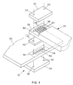
- Fig. 1 is an exploded view of a portion of an interconnection system comprising a RF flex circuit, an elastomeric interconnect and a printed circuit board in accordance with the present invention.
- Figs. 2a and 2b illustrate the side views of an interconnection system in accordance with the present invention.
- Fig. 3 illustrates an example of a circuit board employed in an interconnection system in accordance to the present invention.
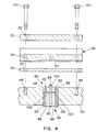
- Fig. 4 illustrates a retrofit application of an interconnection system in accordance with the present invention.
- Fig. 1 illustrates an exploded view of one embodiment of the invention such as an interconnection system 10 that may be employed in a radio frequency (RF) distribution fabric.
- the interconnection system comprises an RF flex circuit 36, a compression interconnect 40, and a radio frequency (RF) board 50.
- RF radio frequency
- RF board 50 may be a printed circuit board having a plurality of radio frequency signal lines or traces, as described in more detail in reference with Figs. 3a and 3b, although the invention is not limited in scope in that respect.
- circuit packs in a wireless base station such as transmitter and receiver and switching circuit packs contain numerous signal lines that carry radio frequency signals.
- Such signal lines are usually made of copper and may be embedded within the material that forms the printed circuit board.
- the signal lines may be disposed on the outer layer of the printed circuit board.
- existing circuit packs may employ coaxial cable connectors for coupling signal lines to coaxial cables.
- circuit board 50 is preferably disposed over a substrate 54.
- This substrate may be made of a rigid material.
- the substrate may be made of an insulating material such as plastic.
- radio frequency signal lines of circuit board 50 may be coupled to compression interconnect 40 via contact pads 56.
- compression interconnect 40 may be made of an elastomeric material.
- Such contact pads may also be coupled to signal lines embedded within the circuit board via through- holes 72 (Fig. 2a) as will be explained in more detail hereinafter.
- annular ground areas 58 may surround contact pads 56 and through-holes 72.
- elastomeric compression interconnect 40 is advantageously positioned over circuit board 50, such that holes 42 of compression interconnect 40 overlay holes 48 of circuit board 50 and holes 52 of substrate 54.
- the design of elastomeric compression interconnects is well-known as described in the United States patent No. 5,045,249 issued to Jin et al. and in the United States patent No. 4,820,376 issued to Lambert et al., both of which are incorporated herein by reference.
- electrical interconnections 46 are made by means of a layer or sheet medium comprising chains of magnetically aligned, electrically conducting particles in a non-conducting matrix material 44.
- Electrically conductive, magnetic particles are aligned into essentially straight chains as resulting from application of a magnetic field in the z-direction of desired conductivity transverse to the x-y plane of interconnect 40. End particles of chains may preferably protrude from a surface of the medium, thereby enhancing electrical contact properties of the medium. Electrical interconnections 46 may be attached to contact pads disposed at both sides of compression interconnect 40.
- the high frequency characteristics of elastomeric compression interconnects such as 40 is one of the factors that is preferably considered in its manufacture.
- an interconnection such as 40 may be made by first mixing a silicone resin material such as RTV615 with 10 volume percent gold-coated nickel spheres having a diameter of about 2 mils. The mixture is spread to form a layer having a thickness of approximately 10 mils. The free surface of the mixture may be left uncovered. A magnetic field having a strength of approximately 400 oersteds is then applied in a direction perpendicular to the layer while the adhesive is cured at approximately 100 ° C.
- the compression interconnect material such as 40 may transmit a signal at about 1.7Gb/s (0.158 ns rise time) with 5.0% reflection or less.
- elastomeric connector materials may include a pad array interconnect known as Matrix MOE connector, and FujiPolymer W-Series materials, which includes wires extending through the thickness of the elastomer. These wires are typically located on a regular grid.
- compression interconnects may be employed such as Interposer and Micro-Interposer brands manufactured by AMP. These products are micro-mechanical contacts which require 300 grams and 150 grams force per contact, respectively, to form a reliable interconnect.
- Other examples include EII and PAI brands manufactured by AUGAT. These products are designed for 50-mil centerline pad array interconnection.
- EII is constructed from a flexible circuit and utilizes through-hole technology, while PAI is made from miniature compression mountable spring plungers.
- the compression interconnect meet the electrical design specifications relating to the particular applications employed in connection with the present invention.
- not all elastomeric compression interconnect materials are suitable for RF applications.
- the magnetically aligned materials employed in the present invention and described previously have shown to be advantageously useable at frequencies up to about 4GHz--which is an approximate frequency limit for testing purposes.
- a flex circuit 36 is positioned over compression interconnect 40, such that holes 38 of the flex circuit overlay holes 42, 48 and 52.
- Signal lines 30 are embedded within flex circuit 36 and are configured to carry radio frequency signals.
- the length of flex circuit 36 depends on requirements of the particular radio frequency RF distribution fabric to be implemented. Preferably, when the RF distribution fabric is implemented in a wireless base station of a wireless telecommunications system, the length of the flex circuit may be about 20 inches long.
- Signal lines 30 are preferably made of copper, and are embedded in a flexible dielectric material 26.
- the loss of radio frequency signals carried in signal lines 30 depends on, among other things, the dielectric constant and the dielectric dissipation factor.
- flex circuit 36 may advantageously include interstitial ground lines 28 positioned adjacent to signal lines 30, although the invention is not limited in scope in that respect.
- the use of ground lines 28 may substantially reduce cross talk between signal lines 30.
- Signal lines 30 and ground lines 28 are preferably situated between two ground planes disposed on the outer surface of dielectric 26.
- contact pads for coupling conductors 47 and signal lines 30 are preferably situated on the one surface of flex circuit 36 positioned against compression interconnect 50.
- a cover 20 is positioned over flex circuit 36, such that holes 22 overlay holes 38. Cover 20 is advantageously made of an insulating material.
- a screw 120 (Fig. 4) may run through holes 22, 38, 42, 48 and 52, to attach the circuit board signal lines and the flex circuit signal lines via compression interconnect 40. It is noted that other suitable means of attachment, such as clamping or bonding may also be employed.
- Figs. 2a and 2b illustrate the side views of one embodiment of an interconnection system 10 in accordance with the present invention, although the invention is not limited in scope to this embodiment.
- Flex circuit 36 comprises a ground plane 84 disposed over the internal section of a solder mask layer 86.
- a dielectric layer 26 is disposed over ground layer 84.
- Dielectric layer 26 comprises a flexible substrate and is formed from multiple layers.
- An exemplary signal line 88 is preferably embedded within the dielectric layer. In this particular context, signal line 88 is positioned along an axis perpendicular to the plane of the paper.
- a ground layer 82 is disposed over dielectric layer 26. Ground layer 82 is configured so as to form openings 94.
- a contact pad 92 is disposed over dielectric 26, and is coupled to signal line 88 via a through-hole 90. Contact pad 92 is preferably made of gold-plated copper.
- a solder mask layer 80 is disposed over ground layer 82, and is configured so as to form openings 96.
- Compression interconnect 40 is positioned over flex circuit 36 so as to make contacts with contact pad 92 and ground plane 82 through openings 96.
- Compression interconnect 40 is positioned to also make contact with circuit board 50 as described below.
- Circuit board 50 may be a circuit pack employed in a wireless base station of a wireless telecommunications system, although the invention is not limited in scope in that respect.
- circuit board 50 may be a printed circuit board having radio frequency signal traces. Such signal traces may be disposed on the circuit board.
- signal lines 70 may be embedded within circuit board 50.
- signal line 70 is coupled to a contact pad 74 via a through hole 72.
- Circuit board 50 may preferably include a ground layer 76 disposed over the external surface of circuit board 50, covered by a mask layer 78. Ground layer 76 is configured so as to form openings 98. Likewise, solder mask layer 78 is configured so as to form openings 102.
- signal lines 88 within dielectric 26 have preferably a substantially low signal loss.
- This signal loss is preferably in the order of 0.5 dB, or less, for a 20"- long flex circuit. However, signal losses of about 2 through 4 dB may be sufficiently acceptable.
- Flex circuit 36 is preferably made of a dielectric material with a dielectric constant of about 2 through 4 and a dissipation factor of about 0.005 or less at 1 GHz.
- dielectric 26 may be made of Kapton laminate in conjunction with Arcrylic Bondply both manufactured by DuPont.
- flex circuit 36 may be manufactured in two steps. During the first step, two dielectric layers of Kapton laminate are formed, with a thickness of approximately half of the final thickness of flex circuit 36. On one of the dielectric layers signal lines 88 are formed. Thereafter during the second step, the other half of dielectric layer is bonded to the first half using the Arcrylic Bondply.
- Table 1 illustrates dielectric properties of Kapton and Acrylic Bondply in accordance with one aspect of the invention, although the invention is not limited in scope in this respect.
- flex circuit 36 may be made of Gore-Flex laminate and Speedboard J Bondply, both manufactured by GoreTex. Table 2 illustrates dielectric properties of these materials. Table -2- Dielectric Constant @ 1MHz Dissipation Factor @ 1MHz Gore-Flex laminate 3.1 0.005 Speedboard J Bondply 2.3 0.004
- flex circuit 36 it is desirable to make flex circuit 36 of one dielectric material instead of two. This results in substantially better signal characteristics.
- One approach to manufacture a flex circuit with one dielectric is to fabricate flex circuits using thermoplastic materials. Thin plys of thermoplastic substrate covered by a copper layer is preferably employed, onto which copper signal lines are then patterned, prior to a bonding or laminating process. The thermoplastic plys may then be advantageously laminated to produce a structure in which the signal conductors are embedded within a homogenous dielectric.
- An example of such thermoplastic material is Vectra brand dielectric manufactured by Hoechst-Celanese.
- Table 3 illustrates the electrical characteristics of Vectran, which is a liquid crystal polymer (LCP) product.
- LCP liquid crystal polymer
- thermoplastic materials that may be suitable for use as flex circuit 36 are illustrated in Table 4 below.
- Fig. 2b illustrates another embodiment of interconnection system 10 showing a plurality of signal lines 88 in flex circuit 36 coupled to signal lines 70 in circuit board 50.
- flex circuit 36 include one layer of signal lines, it may be desirable to have multiple layers of signal lines for some applications.
- circuit board 50 may also be made of multiple layers of signal traces.
- Figs. 3a and 3b illustrate an embodiment of circuit board such as 50 in more detail.
- Fig. 3a is a perspective view of circuit board 50 as described in reference with Fig. 1.
- Fig. 3b is a side view illustration of circuit board 50 having a plurality of signal lines 70 embedded within the circuit board and coupled to contact pads 56 via through holes 72.
- Fig. 4 illustrates a circuit board such as 50 having an existing coaxial pin connector 96, which includes a signal pin 92 and annular grounding receptacle 94.
- coaxial pin connector is advantageously modified such that insulating sections 88 are pressed downwardly to below lines 102.
- An adaptor plug 80 is then inserted over coaxial pins 92 and within the annular grounding receptacle 94 of the coaxial connector.
- Plug 80 includes a signal connector 84 topped by a contact pad 104.
- Signal connector 84 couples detachably to pin 92.
- Adaptor plug 80 includes an annular ground ring 82 that couples to ground pins of coaxial connector 96.
- the annular ground ring 82 along with contact pad 104 may then be coupled to compression interconnect 40 to form an interconnection system with flex circuit 36 as described above.
- the present invention allows substantial cost savings for implementing radio frequency distribution fabrics over prior art interconnection systems. Furthermore, the present invention allows the possibility of substantially miniaturizing such radio frequency distribution fabrics.
Landscapes
- Engineering & Computer Science (AREA)
- Metallurgy (AREA)
- Manufacturing & Machinery (AREA)
- Microelectronics & Electronic Packaging (AREA)
- Combinations Of Printed Boards (AREA)
- Coupling Device And Connection With Printed Circuit (AREA)
- Multi-Conductor Connections (AREA)
Applications Claiming Priority (2)
| Application Number | Priority Date | Filing Date | Title |
|---|---|---|---|
| US08/623,087 US5795162A (en) | 1996-03-28 | 1996-03-28 | RF flex circuit transmission line and interconnection method |
| US623087 | 1996-03-28 |
Publications (2)
| Publication Number | Publication Date |
|---|---|
| EP0798802A2 true EP0798802A2 (de) | 1997-10-01 |
| EP0798802A3 EP0798802A3 (de) | 1998-10-28 |
Family
ID=24496715
Family Applications (1)
| Application Number | Title | Priority Date | Filing Date |
|---|---|---|---|
| EP97301801A Withdrawn EP0798802A3 (de) | 1996-03-28 | 1997-03-18 | Übertragungsleitung für flexible Schaltung und Verbindungsverfahren |
Country Status (5)
| Country | Link |
|---|---|
| US (1) | US5795162A (de) |
| EP (1) | EP0798802A3 (de) |
| JP (1) | JPH1069931A (de) |
| KR (1) | KR100242214B1 (de) |
| TW (1) | TW457835B (de) |
Cited By (4)
| Publication number | Priority date | Publication date | Assignee | Title |
|---|---|---|---|---|
| WO2005046005A1 (en) * | 2003-11-05 | 2005-05-19 | Tensolite Company | Zero insertion force high frequency connector |
| WO2006127521A1 (en) * | 2005-05-20 | 2006-11-30 | Tensolite Company | High frequency connector assembly |
| US7503768B2 (en) | 2003-11-05 | 2009-03-17 | Tensolite Company | High frequency connector assembly |
| EP2887452A1 (de) * | 2013-12-18 | 2015-06-24 | Arvind Swarup | Übertragungsleitungsschaltungsanordnungen und Verfahren zur Herstellung |
Families Citing this family (30)
| Publication number | Priority date | Publication date | Assignee | Title |
|---|---|---|---|---|
| WO1997001437A1 (en) * | 1995-06-28 | 1997-01-16 | Fraivillig Materials Company | Circuit board laminates and method of making |
| US6139337A (en) * | 1997-11-26 | 2000-10-31 | General Electric Company | Elastomeric connection for computed tomography system |
| US6867948B1 (en) * | 1999-01-22 | 2005-03-15 | Seagate Technology Llc | Disc drives having flexible circuits with liquid crystal polymer dielectric |
| US6241532B1 (en) * | 1999-06-25 | 2001-06-05 | Exatron, Inc. | High density electrical connector assembly and connector for use therewith |
| US7223105B2 (en) * | 1999-12-16 | 2007-05-29 | Paricon Technologies Corporation | Cable connector incorporating anisotropically conductive elastomer |
| US6628182B1 (en) * | 2000-01-26 | 2003-09-30 | Anritsu Company | Right angle coaxial cable connections to microwave components on a carrier |
| US6639154B1 (en) * | 2000-10-10 | 2003-10-28 | Teradyne, Inc. | Apparatus for forming a connection between a circuit board and a connector, having a signal launch |
| JP3851075B2 (ja) * | 2000-10-26 | 2006-11-29 | インターナショナル・ビジネス・マシーンズ・コーポレーション | コンピュータシステム、電子回路基板およびカード |
| US6758681B2 (en) * | 2002-07-01 | 2004-07-06 | Morgan T. Johnson, Jr. | Electrical cable interconnections for reduced impedance mismatches |
| JP2004146400A (ja) * | 2002-10-21 | 2004-05-20 | Hosiden Corp | プリント基板とフレキシブル基板との接続構造 |
| US6699054B1 (en) | 2003-01-15 | 2004-03-02 | Applied Engineering Products, Inc. | Float mount coaxial connector |
| JP3888990B2 (ja) * | 2003-10-22 | 2007-03-07 | ジーイー・メディカル・システムズ・グローバル・テクノロジー・カンパニー・エルエルシー | コネクタおよび放射線断層撮影装置 |
| US7282932B2 (en) * | 2004-03-02 | 2007-10-16 | Micron Technology, Inc. | Compliant contact pin assembly, card system and methods thereof |
| US20070137032A1 (en) * | 2005-12-15 | 2007-06-21 | Braden Stephen M | Ground stud installation on composite structure for electrostatic charges |
| US7886439B2 (en) * | 2005-12-15 | 2011-02-15 | The Boeing Company | Ground stud installation on composite structures for electrostatic charges |
| US7672142B2 (en) * | 2007-01-05 | 2010-03-02 | Apple Inc. | Grounded flexible circuits |
| US20090226696A1 (en) * | 2008-02-06 | 2009-09-10 | World Properties, Inc. | Conductive Polymer Foams, Method of Manufacture, And Uses Thereof |
| US8623265B2 (en) * | 2007-02-06 | 2014-01-07 | World Properties, Inc. | Conductive polymer foams, method of manufacture, and articles thereof |
| WO2008097571A1 (en) * | 2007-02-06 | 2008-08-14 | World Properties, Inc. | Conductive polymer foams, method of manufacture, and uses thereof |
| US20090010598A1 (en) * | 2007-06-27 | 2009-01-08 | Feeney Christopher J | In-situ electrical connector with composite structure |
| EP2519568A1 (de) * | 2009-12-29 | 2012-11-07 | Rogers Corporation | Leitende polymerschaumstoffe, herstellungsverfahren und ihre verwendung |
| CN102378501B (zh) * | 2010-07-13 | 2013-06-26 | 富葵精密组件(深圳)有限公司 | 电路板制作方法 |
| CN102340938B (zh) * | 2010-07-29 | 2013-08-28 | 富葵精密组件(深圳)有限公司 | 电路板制作方法 |
| JP5765161B2 (ja) * | 2011-09-16 | 2015-08-19 | 日立金属株式会社 | 差動信号伝送用ケーブルの特性評価機構及び特性評価方法 |
| US9059545B2 (en) * | 2012-07-11 | 2015-06-16 | Tyco Electronics Corporations | Socket connectors and methods of assembling socket connectors |
| KR102609194B1 (ko) * | 2016-03-10 | 2023-12-05 | 삼성전자 주식회사 | 커넥터 및 이를 포함하는 전자 장치 |
| CN109449617B (zh) * | 2018-11-20 | 2023-10-20 | 惠州硕贝德无线科技股份有限公司 | 一种射频连接结构 |
| US12100920B2 (en) | 2019-12-19 | 2024-09-24 | Zomedica Biotechnologies Llc | Coaxial connector |
| KR102790199B1 (ko) * | 2021-01-05 | 2025-04-03 | 주식회사 엘지에너지솔루션 | 연결 구조 |
| WO2022176631A1 (ja) * | 2021-02-17 | 2022-08-25 | 株式会社ヨコオ | 接続装置 |
Family Cites Families (13)
| Publication number | Priority date | Publication date | Assignee | Title |
|---|---|---|---|---|
| US4268956A (en) * | 1977-10-13 | 1981-05-26 | Bunker Ramo Corporation | Method of fabricating an interconnection cable |
| US4534602A (en) * | 1982-05-26 | 1985-08-13 | Fairchild Camera & Instrument Corp. | R.F. multi-pin connector |
| US4684200A (en) * | 1985-11-12 | 1987-08-04 | Amp Incorporated | Press fit cable termination for printed circuit boards |
| US5045249A (en) * | 1986-12-04 | 1991-09-03 | At&T Bell Laboratories | Electrical interconnection by a composite medium |
| US4695258A (en) * | 1986-12-09 | 1987-09-22 | Cherne Industries, Inc. | Connector assembly for electrically connecting flexible and rigid printed circuits |
| US4820376A (en) * | 1987-11-05 | 1989-04-11 | American Telephone And Telegraph Company At&T Bell Laboratories | Fabrication of CPI layers |
| US5041015A (en) * | 1990-03-30 | 1991-08-20 | Cal Flex, Inc. | Electrical jumper assembly |
| JPH04315491A (ja) * | 1991-04-12 | 1992-11-06 | Fujikura Ltd | プリント配線板 |
| US5148135A (en) * | 1991-09-04 | 1992-09-15 | Raytheon Company | Electronic hardware package |
| US5145382A (en) * | 1991-11-29 | 1992-09-08 | Motorola, Inc. | Molded plastic surface-mountable coaxial connector |
| DE69306600T2 (de) * | 1992-01-17 | 1997-04-17 | Fujitsu Ltd | Verfahren zur Herstellung eines mehrschichtigen Leitersubstrats |
| US5244395A (en) * | 1992-07-29 | 1993-09-14 | Motorola, Inc. | Circuit interconnect system |
| US5479110A (en) * | 1994-01-13 | 1995-12-26 | Advanpro Corporation | Printed flexible circuit terminations and method of manufacture |
-
1996
- 1996-03-28 US US08/623,087 patent/US5795162A/en not_active Expired - Fee Related
-
1997
- 1997-01-28 TW TW086100939A patent/TW457835B/zh not_active IP Right Cessation
- 1997-03-18 EP EP97301801A patent/EP0798802A3/de not_active Withdrawn
- 1997-03-21 JP JP9068143A patent/JPH1069931A/ja active Pending
- 1997-03-27 KR KR1019970012126A patent/KR100242214B1/ko not_active Expired - Fee Related
Cited By (10)
| Publication number | Priority date | Publication date | Assignee | Title |
|---|---|---|---|---|
| WO2005046005A1 (en) * | 2003-11-05 | 2005-05-19 | Tensolite Company | Zero insertion force high frequency connector |
| US7074047B2 (en) | 2003-11-05 | 2006-07-11 | Tensolite Company | Zero insertion force high frequency connector |
| US7249953B2 (en) | 2003-11-05 | 2007-07-31 | Tensolite Company | Zero insertion force high frequency connector |
| US7404718B2 (en) | 2003-11-05 | 2008-07-29 | Tensolite Company | High frequency connector assembly |
| US7503768B2 (en) | 2003-11-05 | 2009-03-17 | Tensolite Company | High frequency connector assembly |
| US7748990B2 (en) | 2003-11-05 | 2010-07-06 | Tensolite, Llc | High frequency connector assembly |
| US7997907B2 (en) | 2003-11-05 | 2011-08-16 | Tensolite, Llc | High frequency connector assembly |
| WO2006127521A1 (en) * | 2005-05-20 | 2006-11-30 | Tensolite Company | High frequency connector assembly |
| EP2887452A1 (de) * | 2013-12-18 | 2015-06-24 | Arvind Swarup | Übertragungsleitungsschaltungsanordnungen und Verfahren zur Herstellung |
| US9634371B2 (en) | 2013-12-18 | 2017-04-25 | Com Dev International Ltd. | Transmission line circuit assemblies and processes for fabrication |
Also Published As
| Publication number | Publication date |
|---|---|
| KR970068023A (ko) | 1997-10-13 |
| TW457835B (en) | 2001-10-01 |
| KR100242214B1 (ko) | 2000-02-01 |
| US5795162A (en) | 1998-08-18 |
| JPH1069931A (ja) | 1998-03-10 |
| EP0798802A3 (de) | 1998-10-28 |
Similar Documents
| Publication | Publication Date | Title |
|---|---|---|
| US5795162A (en) | RF flex circuit transmission line and interconnection method | |
| US7223105B2 (en) | Cable connector incorporating anisotropically conductive elastomer | |
| KR100511814B1 (ko) | 혼합 신호 인쇄 배선 보드 상의 단일 조립체를 위한저비용, 대용량의 rf 혼성 패키지 | |
| EP1097488B1 (de) | Hf-verbinder | |
| US7180394B2 (en) | Millimeter wave (MMW) radio frequency transceiver module and method of forming same | |
| US5308250A (en) | Pressure contact for connecting a coaxial shield to a microstrip ground plane | |
| US5477159A (en) | Integrated circuit probe fixture with detachable high frequency probe carrier | |
| US6930240B1 (en) | Flex-circuit shielded connection | |
| US11879934B2 (en) | Test kit for testing a device under test | |
| CN115133339B (zh) | 线缆组件、信号传输组件及通信系统 | |
| US6407652B1 (en) | Adapters for RF connectors | |
| US6864696B2 (en) | High density, high frequency, board edge probe | |
| JP3266280B2 (ja) | 一体化された環境的シールを有する圧縮可能な同軸相互接続 | |
| US20040253870A1 (en) | Electrical cable interconnections for reduced impedance mismatches | |
| CN111031667B (zh) | 一种微波信号垂直互连装置及互连方法 | |
| JP4387943B2 (ja) | 相互接続システム | |
| US12352781B2 (en) | Test kit for testing a device under test | |
| JP2549125Y2 (ja) | 電気接続用コネクタ | |
| WO2006062911A1 (en) | Test socket and method for making | |
| US20210045244A1 (en) | Multiple circuit boards with high-density compression interconnect | |
| WO2000008675A2 (en) | Adapter for surface mounted devices | |
| US20250316918A1 (en) | System and method for non-planar connectors | |
| WO2005018056A1 (en) | Cable connector incorporating anisotropically conductive elastomer | |
| KR200157893Y1 (ko) | 경연성 다층 인쇄회로기판 | |
| WO2025259903A1 (en) | Direct connection apparatus and method |
Legal Events
| Date | Code | Title | Description |
|---|---|---|---|
| PUAI | Public reference made under article 153(3) epc to a published international application that has entered the european phase |
Free format text: ORIGINAL CODE: 0009012 |
|
| AK | Designated contracting states |
Kind code of ref document: A2 Designated state(s): DE FR GB SE |
|
| PUAL | Search report despatched |
Free format text: ORIGINAL CODE: 0009013 |
|
| AK | Designated contracting states |
Kind code of ref document: A3 Designated state(s): DE FR GB SE |
|
| 17P | Request for examination filed |
Effective date: 19990415 |
|
| 17Q | First examination report despatched |
Effective date: 20021106 |
|
| STAA | Information on the status of an ep patent application or granted ep patent |
Free format text: STATUS: THE APPLICATION IS DEEMED TO BE WITHDRAWN |
|
| 18D | Application deemed to be withdrawn |
Effective date: 20030318 |