EP0796505B1 - Plasmareaktor und verfahren zu dessen betrieb - Google Patents
Plasmareaktor und verfahren zu dessen betrieb Download PDFInfo
- Publication number
- EP0796505B1 EP0796505B1 EP95940142A EP95940142A EP0796505B1 EP 0796505 B1 EP0796505 B1 EP 0796505B1 EP 95940142 A EP95940142 A EP 95940142A EP 95940142 A EP95940142 A EP 95940142A EP 0796505 B1 EP0796505 B1 EP 0796505B1
- Authority
- EP
- European Patent Office
- Prior art keywords
- plasma
- plasma reactor
- exciting
- counter electrode
- wafer holder
- Prior art date
- Legal status (The legal status is an assumption and is not a legal conclusion. Google has not performed a legal analysis and makes no representation as to the accuracy of the status listed.)
- Expired - Lifetime
Links
- 238000000034 method Methods 0.000 title claims description 35
- 239000000758 substrate Substances 0.000 claims description 18
- 238000004088 simulation Methods 0.000 claims description 6
- 238000005259 measurement Methods 0.000 claims description 4
- 230000013011 mating Effects 0.000 claims 9
- 230000008021 deposition Effects 0.000 description 18
- 238000005530 etching Methods 0.000 description 16
- 238000006243 chemical reaction Methods 0.000 description 15
- 239000007789 gas Substances 0.000 description 11
- 230000005284 excitation Effects 0.000 description 10
- 235000012431 wafers Nutrition 0.000 description 5
- 238000004364 calculation method Methods 0.000 description 4
- XUIMIQQOPSSXEZ-UHFFFAOYSA-N Silicon Chemical compound [Si] XUIMIQQOPSSXEZ-UHFFFAOYSA-N 0.000 description 3
- 229910021417 amorphous silicon Inorganic materials 0.000 description 3
- 239000010453 quartz Substances 0.000 description 3
- 229910052710 silicon Inorganic materials 0.000 description 3
- 239000010703 silicon Substances 0.000 description 3
- VYPSYNLAJGMNEJ-UHFFFAOYSA-N silicon dioxide Inorganic materials O=[Si]=O VYPSYNLAJGMNEJ-UHFFFAOYSA-N 0.000 description 3
- 230000008878 coupling Effects 0.000 description 2
- 238000010168 coupling process Methods 0.000 description 2
- 238000005859 coupling reaction Methods 0.000 description 2
- 239000013078 crystal Substances 0.000 description 2
- 238000005516 engineering process Methods 0.000 description 2
- 238000011156 evaluation Methods 0.000 description 2
- 230000001939 inductive effect Effects 0.000 description 2
- 229910021420 polycrystalline silicon Inorganic materials 0.000 description 2
- 229920005591 polysilicon Polymers 0.000 description 2
- 239000004065 semiconductor Substances 0.000 description 2
- 238000012360 testing method Methods 0.000 description 2
- 238000013459 approach Methods 0.000 description 1
- 238000011065 in-situ storage Methods 0.000 description 1
- 239000012212 insulator Substances 0.000 description 1
- 150000002500 ions Chemical class 0.000 description 1
- 238000002955 isolation Methods 0.000 description 1
- 238000004519 manufacturing process Methods 0.000 description 1
- 239000002184 metal Substances 0.000 description 1
- 238000011017 operating method Methods 0.000 description 1
- 238000013386 optimize process Methods 0.000 description 1
- 238000001020 plasma etching Methods 0.000 description 1
- 238000012545 processing Methods 0.000 description 1
Images


Classifications
-
- H—ELECTRICITY
- H01—ELECTRIC ELEMENTS
- H01J—ELECTRIC DISCHARGE TUBES OR DISCHARGE LAMPS
- H01J37/00—Discharge tubes with provision for introducing objects or material to be exposed to the discharge, e.g. for the purpose of examination or processing thereof
- H01J37/32—Gas-filled discharge tubes
- H01J37/32009—Arrangements for generation of plasma specially adapted for examination or treatment of objects, e.g. plasma sources
- H01J37/32082—Radio frequency generated discharge
-
- H—ELECTRICITY
- H01—ELECTRIC ELEMENTS
- H01J—ELECTRIC DISCHARGE TUBES OR DISCHARGE LAMPS
- H01J37/00—Discharge tubes with provision for introducing objects or material to be exposed to the discharge, e.g. for the purpose of examination or processing thereof
- H01J37/32—Gas-filled discharge tubes
- H01J37/32431—Constructional details of the reactor
- H01J37/32532—Electrodes
-
- H—ELECTRICITY
- H01—ELECTRIC ELEMENTS
- H01J—ELECTRIC DISCHARGE TUBES OR DISCHARGE LAMPS
- H01J2237/00—Discharge tubes exposing object to beam, e.g. for analysis treatment, etching, imaging
- H01J2237/32—Processing objects by plasma generation
- H01J2237/33—Processing objects by plasma generation characterised by the type of processing
- H01J2237/332—Coating
- H01J2237/3322—Problems associated with coating
- H01J2237/3323—Problems associated with coating uniformity
-
- H—ELECTRICITY
- H01—ELECTRIC ELEMENTS
- H01J—ELECTRIC DISCHARGE TUBES OR DISCHARGE LAMPS
- H01J2237/00—Discharge tubes exposing object to beam, e.g. for analysis treatment, etching, imaging
- H01J2237/32—Processing objects by plasma generation
- H01J2237/33—Processing objects by plasma generation characterised by the type of processing
- H01J2237/334—Etching
- H01J2237/3343—Problems associated with etching
Definitions
- a low-pressure plasma is in the plasma reactors generated in which reactive ions are present, the the surface of a substrate located in the reactor Initiate an etching reaction or a deposition reaction.
- the plasma reactor become both etching processes and layer deposits of insulators, metal layers, semiconductor layers and similar carried out.
- the plasma is different in different plasma reactors excited.
- the plasma is excited between two electrodes, one of which one grounded, the other capacitive with high frequency voltage connected is.
- the substrate to be processed is in the parallel plate reactor placed on the grounded electrode.
- a plasma reactor is known in the art is referred to as an ICP reactor.
- A is in the ICP reactor Plasma ignited by inductive coupling of electrical energy.
- the ICP reactor comprises a disk holder Recording of the substrate to be processed, for example is grounded.
- There is an antenna opposite the window holder arranged facing the inner wall of the ICP reactor Example is insulated by an insulating layer. over the antenna inductively becomes a radio frequency field in the reactor coupled.
- the invention has for its object a plasma reactor specify in which the homogeneity of the process rate over the Diameter of the plasma reactor compared to the prior art is improved. Furthermore, it is an object of the invention to specify an operating method for such a plasma reactor.
- this object is achieved by a plasma reactor according to claim 1 or 3 and a method for its operation according to claim 5. Further embodiments of the invention emerge from the subclaims.
- the plasma is turned on in the plasma reactor according to the invention different positions above one to be processed Substrate excited differently. This can cause inhomogeneities of process rates, on the one hand due to an inhomogeneity of the plasma itself and on the other hand to an inhomogeneous one Consumption of reactive gas molecules can be reduced, be balanced.
- the plasma reactor comprises a device for plasma excitation by coupling electrical energy that at least two independently controllable sub-devices includes.
- the device comprises for plasma excitation at least one with a reference potential connected electrode and a counter electrode arrangement.
- the Counter-electrode arrangement has at least two or counter electrode elements that can be controlled independently of one another on.
- the device also includes plasma excitation a high-frequency voltage source for each counter-electrode element, the capacitive with the respective counter electrode element connected is. Between those connected with reference potential The electrode and each counter electrode element takes place Excitation of a plasma.
- Each counter electrode element that assigned high-frequency voltage source and the one with reference potential connected electrode forms a sub-device for plasma excitation.
- the disc holder for the process to be processed in this embodiment is between those with reference potential connected electrode and the counter electrode arrangement arranged.
- the disc holder can be used on both with reference potential connected electrode as well as on a of the counter electrode elements.
- one of the counter electrode elements is advantageous to use one of the counter electrode elements to form a circle and that or to form the further counter electrode elements in a ring shape.
- the circular counter electrode element and the or annular counter electrode elements are concentric in arranged on one level. Through these circular / ring-shaped counter electrode elements become inhomogeneities in a cylinder geometry, like when using disc-shaped Substrates, optimally balanced.
- the counter-electrode elements Indicates the plasma reactor and / or the one to be processed Another symmetry, it is within the scope of the Invention, the counter-electrode elements with a different geometry, for example as sectors of a circle.
- the plasma reactor comprises as a device for plasma excitation with an antenna arrangement two or more antennas via which the plasma excitation is inductive he follows. Each antenna is connected to it AC power source provided. Antenna and AC power source each form a sub-facility.
- the plasma reactor corresponds in this embodiment, the one known as the ICP reactor Type.
- the antennas essentially to form a ring with a different radius and arranged concentrically on one level.
- the control of the partial devices for plasma excitation takes place in the simplest way by determining the parameters for the individual sub-devices via calibration measurements. To do this Test series with different parameter settings for the control of the sub-devices carried out.
- control the partial devices to optimize for plasma excitation in situ.
- a control unit the sub-devices controlled.
- an ellipsometer is suitable for the process variable.
- quartz crystals such as those used for layer deposition used for thickness control.
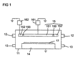
- a plasma reactor comprises a reaction chamber 11 which Pump nozzle 12 and gas supply lines 13 for the supply of Process gas has (see Figure 1).
- the reaction chamber 11 is connected to a reference potential, for example earth potential.
- a disk holder 14 is provided in the reaction chamber 11, which is also at the reference potential.
- the disc holder For example, 14 is cylindrical and has one Diameter of 200 mm.
- the Disk holder 14 is an electrode at reference potential.
- the counter electrode arrangement 15 comprises a first counter electrode element 151 and a second counter electrode element 152.
- the first counter electrode element 151 is circular with a diameter of, for example, 200 mm.
- the second counter electrode element 152 is ring-shaped, for example, the width of the ring is 30 mm.
- the second counter electrode element 152 is concentric with the first counter electrode element 151 arranged in one plane. Between the first counter electrode element 151 and the second counter electrode element 152 is a gap 150 in one Width of 1 mm, for example.
- the distance between the Counter electrode arrangement 15 and the disc holder 14 is for example 41 mm.
- Each of the counter electrode elements 151, 152 is capacitive with each connected to a high-frequency voltage source 161, 162.
- the high-frequency voltage sources 161, 162 are independent adjustable from each other.
- the amplitude or the phase the electrode control can be varied. They are also independent Variations in the drive frequency or the impressed DC component possible.
- this plasma reactor is the homogeneity of what is carried out Process about the diameter of one on the disc holder 14 arranged substrate wafer 17 by independent control of the first counter electrode element 151 and second counter electrode element 152 adjustable.
- the optimized parameters are, for example, by advance carried out test series determined.
- the homogeneity of the process via trial processed slices depending on the counter electrode elements 151, 152 created parameters determined.
- the plasma reactor explained with reference to FIG. 1 is suitable, for example, for the deposition of amorphous silicon.
- SiH 4 with a flow rate of 50 sccm is used as process gas.
- a pressure p of 20 Pa is set in the reactor chamber.
- the temperature in the reactor is 350 ° C during the deposition.
- the first counter electrode element 151 and the second counter electrode element 152 are driven independently of one another.
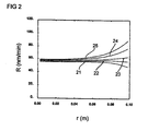
- FIG. 2 shows the result of a simulation calculation for the example of the amorphous silicon deposition for the deposition rate R as a function of the radial distance r.
- the voltage applied to the first counter electrode element is 100 volts each, while the voltage on the second counter electrode element 152 varies between 60 and 160 volts.
- Curve Voltage on the first counter-electrode element 151 Voltage at the second counter electrode element 152 Radio frequency 21 100 volts 60 volts 13.56 MHz 22 100 volts 80 volts 13.56 MHz 23 100 volts 100 volts 13.56 MHz 24th 100 volts 125 volts 13.56 MHz 25th 100 volts 150 volts 13.56 MHz
- FIG. 3 shows the corresponding result of a simulation calculation for the deposition of amorphous silicon for the deposition rate R as a function of the radial distance r from the center.
- the voltage applied to the first counter electrode element 151 has been varied, while the voltage applied to the second counter electrode element 152 is fixed.
- Curve Voltage on the first counter-electrode element 151 Voltage at the second counter electrode element 152 Radio frequency 31 100 volts 100 volts 13.56 MHz 32 125 volts 100 volts 13.56 MHz 33 150 volts 100 volts 13.56 MHz
- a plasma reactor comprises a reaction chamber 41, the pump nozzle 42 and Gas feeds 43 is provided for the admission of process gases (see Figure 4).
- the reaction chamber 41 has a reference potential, for example earth.
- a disk holder 44 is provided in the reaction chamber 41, which is also connected to the reference potential.
- disc holder 44 is cylindrical and has a diameter of 200 mm. In the operation of the plasma reactor is the disc holder 44 as an electrode that with Reference potential is used.
- the disc holder 44 Opposite the disc holder 44 is a counter electrode arrangement 45 arranged. It comprises a first counter electrode element 451, a second counter electrode element 452 and a third counter electrode element 453. All three counter electrode elements 451, 452, 453 are arranged in one plane.
- the first counter electrode element is circular and has one Diameter of, for example, 100 mm.
- the second counter electrode element is ring-shaped and has an outer diameter of, for example, 200 mm.
- the third counter electrode element 453 is also ring-shaped with an outer diameter of, for example, 250 mm.
- Between the first counter electrode element 451 and the second counter electrode element 452 as well between the second counter electrode element 452 and the third Counter electrode element 453 has a gap 450 with it a width of 2 mm is provided. Between the counter electrode arrangement 45 and the disc holder 44 is the distance 80 mm.
- Each of the counter electrode elements 451, 452, 453 is capacitive connected to a high-frequency voltage source 461, 462, 463, which can be controlled independently of each other.
- the counter electrode elements are connected via the high voltage sources 461, 462, 463 451, 452, 453 controlled independently of each other.
- Measuring devices 481, 482, 483 are located in the reaction chamber 41 provided that, for example, three points on the surface a substrate disk 47 are directed, which in the operation of the Plasma reactor is arranged on the disc holder 44.
- the Measuring devices 481, 482, 483 measure a size that the Process in the plasma reactor is subjected. Becomes the plasma reactor used for etching, so are on the measuring devices 481, 482, 483 each the remaining layer thickness on the Measuring points registered. In contrast, becomes one in the plasma reactor Deposition is carried out, so the current layer thickness registered at the measuring points.
- the measuring devices 481, 482, 483 for example as quartz crystal or ellipsometer educated.
- the measuring devices 481, 482, 483 have outputs which are connected to inputs of a control unit 49.
- the Control unit 49 also has outputs, each with a control input of the high frequency voltage sources 461, 462, 463 are connected.
- the control unit 49 comprises for example a microprocessor, in which an evaluation of the data recorded by the measuring devices 481, 482, 483 he follows. Depending on this evaluation, the high-frequency voltage sources 461, 462, 463 control signals given, for an immediate adjustment of the electrode control to lead.
- the plasma reactor explained with reference to FIG. 4 can be used, for example, for etching polysilicon.
- the following process gas Cl 2 with a flow rate of 70 sccm (standard cubic centimeters per minute) is used for this.
- the pressure in the plasma reactor is 16 Pa (120 mTorr), the temperature is 300 K.
- the following powers are coupled to the counter electrode arrangement 45: first counter electrode element 451 200 W. second counter electrode element 452 250 W. third counter electrode element 453 300 W.
- the AC voltage has a high frequency of 13.56 MHz.
- the reaction chamber 51 in another embodiment, includes a plasma reactor a reaction chamber 51, the pump nozzle 52 and gas supplies 53 is provided for a process gas (see figure 5).
- the reaction chamber 51 is at a reference potential to Example zero potential, connected.
- a disc holder 54 is arranged in the reaction chamber 51, the one for receiving substrate wafers 57 Diameter up to 200 mm is suitable.
- the disc holder 54 is also connected to the reference potential.
- An antenna arrangement 55 is provided in the reaction chamber.
- the antenna arrangement 55 comprises mutually independent Antennas 551, 552, 553, which are in an isolation structure 550 made of quartz, for example.
- Each of the antennas 551, 552, 553 is with an AC power source 561, 562, 563 connected.
- the antennas 551, 552, 553 are each essentially ring-shaped and concentric in one plane arranged.
- the first antenna 551 has a diameter of, for example, 100 mm
- the second antenna 552 has one Diameter of 200 mm
- the third antenna 553 has a diameter of, for example, 250 mm.
- the operation of the plasma reactor is carried out via the antenna arrangement 55 inductively a plasma between the antenna arrangement 55 and the substrate disk 57 excited. Since antennas 551, 552, 553 independently of one another via AC sources 561, 562, 563 are controlled, the plasma is different Locations above the substrate wafer 57 different excited. This ensures homogeneous reaction rates across the entire Substrate disk 57 realized.
- the plasma reactor explained with reference to FIG. 5 corresponds an ICP reactor. It is both for etching and for Layer deposition is suitable.
- polysilicon is etched in this plasma reactor.
- the following process gas Cl 2 with a flow rate of 200 sccm is used for this.
- the pressure in the reaction chamber 51 is 1.33 Pa (10 mTorr), the temperature is 300 K.
- the antennas 551, 552, 553 are controlled with the following electrical data: Antenna 551 1 kW Antenna 552 1.2 kW Antenna 553 1.4 kW
Landscapes
- Physics & Mathematics (AREA)
- Engineering & Computer Science (AREA)
- Plasma & Fusion (AREA)
- Chemical & Material Sciences (AREA)
- Analytical Chemistry (AREA)
- Plasma Technology (AREA)
- ing And Chemical Polishing (AREA)
- Drying Of Semiconductors (AREA)
- Chemical Vapour Deposition (AREA)
Description
- Figur 1
- zeigt einen Plasmareaktor mit zwei Gegenelektrodenelementen.
- Figur 2
- zeigt die Abscheiderate in dem in Figur 1 dargestellten Plasmareaktor für eine feste Spannung an dem einen und eine variable Spannung an dem anderen Gegenelektrodenelement.
- Figur 3
- zeigt die Abscheiderate in dem in Figur 1 gezeigten Plasmareaktor für eine variable Spannung an dem einen und eine feste Spannung an dem anderen Gegenelektrodenelement.
- Figur 4
- zeigt einen Parallelplattenreaktor mit drei Gegenelektrodenelementen und mit Mitteln zur Messung einer dem Prozeß unterworfenen Größe und Mitteln zur Regelung der Ansteuerung der Gegenelektrodenelemente.
- Figur 5
- zeigt einen ICP-Reaktor mit drei Antennen.
| Kurve | Spannung am ersten Gegenelektro-denelement 151 | Spannung am zweiten Gegenelektrodenelement 152 | Hochfrequenz |
| 21 | 100 Volt | 60 Volt | 13,56 MHz |
| 22 | 100 Volt | 80 Volt | 13,56 MHz |
| 23 | 100 Volt | 100 Volt | 13,56 MHz |
| 24 | 100 Volt | 125 Volt | 13,56 MHz |
| 25 | 100 Volt | 150 Volt | 13,56 MHz |
| Kurve | Spannung am ersten Gegenelektro-denelement 151 | Spannung am zweiten Gegenelektrodenelement 152 | Hochfrequenz |
| 31 | 100 Volt | 100 Volt | 13,56 MHz |
| 32 | 125 Volt | 100 Volt | 13,56 MHz |
| 33 | 150 Volt | 100 Volt | 13,56 MHz |
| erstes Gegenelektrodenelement 451 | 200 W |
| zweites Gegenelektrodenelement 452 | 250 W |
| drittes Gegenelektrodenelement 453 | 300 W |
| Antenne 551 | 1 kW |
| Antenne 552 | 1,2 kW |
| Antenne 553 | 1,4 kW |
Claims (7)
- Plasmareaktordadurch gekennzeichnet, daßmit einem Scheibenhalter (14), der mit einem Bezugspotential verbunden ist,mit Pumpstutzen (12),mit Gaszuführungen (13),mit einer geerdeten Elektrode,mit einer Einrichtung (15) zur Plasmaanregung durch Einkopplung elektrischer Energie, die mindestens zwei unabhängig voneinander ansteuerbare Teileinrichtungen (151, 152) umfaßt, über die das Plasma an mindestens zwei verschiedenen Orten über dem Scheibenhalter (14) unterschiedlich anregbar ist,bei dem die Einrichtung zur Plasmaanregung mindestens eine mit einem Bezugspotential verbundene Elektrode (14) und eine Gegenelektrodenanordnung (15) umfaßt, wobei die Gegenelektrodenanordnung (15) mindestens zwei voneinander unabhängig ansteuerbare Gegenelektrodenelemente (151, 152) umfaßt,bei dem der Scheibenhalter (14) zwichen der geerdeten Elektrode und der Gegenelektrodenanordnung (15) angeordnet ist,die Einrichtung zur Plasmaanregung darüber hinaus mindestens zwei Hochfrequenzspannungsquellen (161, 162) umfaßt, die jeweils mit einem der Gegenelektrodenelemente (151, 152) kapazitiv verbunden sind.
- Plasmareaktor nach Anspruch 1,bei dem eines der Gegenelektrodenelemente (151) kreisförmig ausgebildet ist und mindestens eines der weiteren Gegenelektrodenelemente (152) ringförmig ausgebildet ist undbei dem das kreisförmige Gegenelektrodenelement (151) und das ringförmige Gegenelektrodenelement (152) konzentrisch in einer Ebene angeordnet sind.
- Plasmareaktordadurch gekennzeichnet, daßmit einem Scheibenhalter (14), der mit einem Bezugspotential verbunden ist,mit Pumpstutzen (12),mit Gaszuführungen (13),mit einer Einrichtung (15) zur Plasmaanregung durch Einkopplung elektrischer Energie, die mindestens zwei unabhängig voneinander ansteuerbare Teileinrichtungen (151, 152) umfaßt, über die das Plasma an mindestens zwei verschiedenen Orten über dem Scheibenhalter (14) unterschiedlich an regbar ist,die Einrichtung zur Plasmaanregung einer Antennenanordnung (55) mit mindestens zwei Antennen (551, 552, 553) umfaßt, über die elektrische Energie zur Plasmaanregung induktiv eingekoppelt wird,die Einrichtung darüber hinaus mindestens zwei Wechselstromquelle (561, 562, 563) umfaßt, die jeweils mit einer der Antennen (551, 552, 553) verbunden sind,die Antennen (551, 552, 553) jeweils im wesentlichen ringförmig mit unterschiedlichem Radius ausgebildet sind und konzentrisch in einer Ebene angeordnet sind.
- Plasmareaktor nach einem der Ansprüche 1 bis 3,bei dem Mittel (481, 482, 483) zur Bewertung eines im Plasmareaktor ablaufenden Prozesses durch Messung einer dem Prozeß unterworfenen Größe an mehreren Orten eines auf dem Scheibenhalter (44) angeordneten Substrats (47) vorgesehen sind,bei dem Mittel (49) zur Ansteuerung der Teileinrichtungen (451, 452, 453) in Abhängigkeit der Messung vorgesehen sind.
- Verfahren zum Betrieb eines Plasmareaktors nach einem der Ansprüche 1 bis 4,
bei dem die Teileinrichtungen zur Plasmaanregung unterschiedlich angesteuert werden. - Verfahren nach Anspruch 5,bei dem während eines im Plasmareaktor ablaufenden Prozesses eine dem Prozeß unterworfene Größe an mehreren Orten eines auf dem Scheibenhalter angeordneten Substrates gemessen wird undbei dem die Teileinrichtungen zur Plasmaanregung in Abhängigkeit der gemessenen Größe angesteuert werden.
- Verfahren nach Anspruch 6,
bei dem durch Vergleich der gemessenen Größe mit dem entsprechenden Wert einer numerischen Simulation des Plasmareaktors iterativ Parameter zur Ansteuerung der Teileinrichtungen zur Plasmaanregung bestimmt werden.
Applications Claiming Priority (3)
| Application Number | Priority Date | Filing Date | Title |
|---|---|---|---|
| DE4443608A DE4443608C1 (de) | 1994-12-07 | 1994-12-07 | Plasmareaktor und Verfahren zu dessen Betrieb |
| DE4443608 | 1994-12-07 | ||
| PCT/DE1995/001739 WO1996018207A1 (de) | 1994-12-07 | 1995-12-05 | Plasmareaktor und verfahren zu dessen betrieb |
Publications (2)
| Publication Number | Publication Date |
|---|---|
| EP0796505A1 EP0796505A1 (de) | 1997-09-24 |
| EP0796505B1 true EP0796505B1 (de) | 1998-09-09 |
Family
ID=6535196
Family Applications (1)
| Application Number | Title | Priority Date | Filing Date |
|---|---|---|---|
| EP95940142A Expired - Lifetime EP0796505B1 (de) | 1994-12-07 | 1995-12-05 | Plasmareaktor und verfahren zu dessen betrieb |
Country Status (4)
| Country | Link |
|---|---|
| EP (1) | EP0796505B1 (de) |
| JP (1) | JPH10510389A (de) |
| DE (2) | DE4443608C1 (de) |
| WO (1) | WO1996018207A1 (de) |
Families Citing this family (10)
| Publication number | Priority date | Publication date | Assignee | Title |
|---|---|---|---|---|
| US6042686A (en) * | 1995-06-30 | 2000-03-28 | Lam Research Corporation | Power segmented electrode |
| JP3385528B2 (ja) | 1999-07-06 | 2003-03-10 | 日本電気株式会社 | ドライエッチング装置とドライエッチング方法 |
| JP2001155899A (ja) * | 1999-11-25 | 2001-06-08 | Tadahiro Omi | プラズマプロセス装置およびプラズマ装置を用いたプロセス |
| WO2001063642A1 (en) * | 2000-02-25 | 2001-08-30 | Tokyo Electron Limited | Multi-zone rf electrode for capacitive plasma sources |
| JP4202292B2 (ja) * | 2004-03-22 | 2008-12-24 | シャープ株式会社 | プラズマ処理装置 |
| JP4550507B2 (ja) * | 2004-07-26 | 2010-09-22 | 株式会社日立ハイテクノロジーズ | プラズマ処理装置 |
| DE102007052103A1 (de) * | 2007-10-31 | 2009-05-07 | Medizinisches Laserzentrum Lübeck GmbH | Vorrichtung zur schonenden Lasertherapie der Retina |
| AT513190B9 (de) * | 2012-08-08 | 2014-05-15 | Berndorf Hueck Band Und Pressblechtechnik Gmbh | Vorrichtung und Verfahren zur Plasmabeschichtung eines Substrats, insbesondere eines Pressblechs |
| JP6574547B2 (ja) * | 2013-12-12 | 2019-09-11 | 東京エレクトロン株式会社 | プラズマ処理装置及びプラズマ処理方法 |
| KR102790836B1 (ko) * | 2022-08-18 | 2025-04-02 | 한국핵융합에너지연구원 | 용량 결합 플라즈마 발생 장치용 전극, 이를 포함하는 용량 결합 플라즈마 발생 장치 및 용량 결합 플라즈마 균일성 조정 방법 |
Family Cites Families (5)
| Publication number | Priority date | Publication date | Assignee | Title |
|---|---|---|---|---|
| EP0334109B1 (de) * | 1988-03-24 | 1993-06-02 | Siemens Aktiengesellschaft | Verfahren und Vorrichtung zum Herstellen von aus amorphen Silizium-Germanium-Legierungen bestehenden Halbleiterschichten nach der Glimmentladungstechnik, insbesondere für Solarzellen |
| KR910002310A (ko) * | 1988-06-29 | 1991-01-31 | 미다 가쓰시게 | 플라즈마 처리장치 |
| DE3830249A1 (de) * | 1988-09-06 | 1990-03-15 | Schott Glaswerke | Plasmaverfahren zum beschichten ebener substrate |
| DE4242894A1 (de) * | 1992-12-18 | 1994-06-23 | Leybold Ag | Vorrichtung zur Mehrfacheinspeisung von HF-Leistung in Kathodenkörpern |
| GB9321489D0 (en) * | 1993-10-19 | 1993-12-08 | Central Research Lab Ltd | Plasma processing |
-
1994
- 1994-12-07 DE DE4443608A patent/DE4443608C1/de not_active Expired - Fee Related
-
1995
- 1995-12-05 WO PCT/DE1995/001739 patent/WO1996018207A1/de not_active Ceased
- 1995-12-05 DE DE59503549T patent/DE59503549D1/de not_active Expired - Fee Related
- 1995-12-05 JP JP8517248A patent/JPH10510389A/ja active Pending
- 1995-12-05 EP EP95940142A patent/EP0796505B1/de not_active Expired - Lifetime
Also Published As
| Publication number | Publication date |
|---|---|
| JPH10510389A (ja) | 1998-10-06 |
| DE4443608C1 (de) | 1996-03-21 |
| WO1996018207A1 (de) | 1996-06-13 |
| DE59503549D1 (de) | 1998-10-15 |
| EP0796505A1 (de) | 1997-09-24 |
Similar Documents
| Publication | Publication Date | Title |
|---|---|---|
| DE60033312T2 (de) | Plasmabehandlungsvorrichtung und -verfahren | |
| DE69128345T2 (de) | Induktiver plasmareaktor im unteren hochfrequenzbereich | |
| DE69403816T2 (de) | Gerät und Verfahren zu erhöhter induktiver Ankopplung an Plasmen mit reduzierter Zerstäubungskontamination | |
| DE69629588T2 (de) | Segmentierte leistungselektrode | |
| DE69734706T2 (de) | Vorrichtungen zur phasendifferenzsteuerung in einem plasmabehandlungssystem | |
| DE69519008T2 (de) | Plasmareaktor | |
| DE69836857T2 (de) | Gerät und verfahren zur steuerung der ionenenergie und plasmadichte in einer plasma-behandlungsvorrichtung | |
| DE102009027476B4 (de) | Innenkammerelement-Temperatursteuerverfahren, kammerinternes Element, Substratanbringtisch und Plasmabearbeitungsvorrichtungsvorrichtung, die selbigen enthält | |
| US7164236B2 (en) | Method and apparatus for improved plasma processing uniformity | |
| DE69320557T2 (de) | Mehr-Gebiet Plasma-Behandlungsvorrichtung | |
| DE60127232T2 (de) | Lineare antriebsvorrichtung zur anwendung in einer plasmabehandlungsvorrichtung | |
| DE69509248T2 (de) | Gerät und verfahren zur in situ magnetron saübern von plasmareakter-kammern | |
| DE69820041T2 (de) | Verfahren und geraet zur ueberwachung von niederschlaege auf der innenoberflaeche einer plasmabarbeitungskammer | |
| DE69028650T2 (de) | Plasma-Ätzmethode | |
| DE212007000107U1 (de) | Ringförmige Plasmakammer für Prozesse mit hohen Gasdurchflussraten | |
| JP2003529216A (ja) | 複合セグメント電極に供給される電力を制御するための方法並びに装置 | |
| DE4443608C1 (de) | Plasmareaktor und Verfahren zu dessen Betrieb | |
| DE69118035T2 (de) | Plasmagerät, Verfahren und Vorrichtung zur Extrahierung eines elektrischen Signals aus einem einer Hochfrequenzwelle ausgesetzten Glied | |
| DE69903301T2 (de) | Fenster hoher zerstäubungs- und ätz-festigkeit für plasma behandlungskammern | |
| DE69030347T2 (de) | Plasmaprozess, Verfahren und Gerät | |
| DE60130744T2 (de) | Induktiv gekoppeltes Plasma-Ätzgerät mit aktiver Steuerung der RF-Spitzenspannung | |
| DE69825112T2 (de) | Verfahren zur Durchführung von Planarisierungs- und Grabensätzung und Vorrichtung dafür | |
| DE69603569T2 (de) | Verfahren zur Substratschadensreduzierung bei PECVD | |
| DE102016102577A1 (de) | Prozessierung von Halbleitervorrichtungen | |
| WO2012119700A1 (de) | Vorrichtung und verfahren zum plasmaunterstützten behandeln zumindest zweier substrate |
Legal Events
| Date | Code | Title | Description |
|---|---|---|---|
| PUAI | Public reference made under article 153(3) epc to a published international application that has entered the european phase |
Free format text: ORIGINAL CODE: 0009012 |
|
| 17P | Request for examination filed |
Effective date: 19970701 |
|
| AK | Designated contracting states |
Kind code of ref document: A1 Designated state(s): DE FR GB IT |
|
| GRAG | Despatch of communication of intention to grant |
Free format text: ORIGINAL CODE: EPIDOS AGRA |
|
| GRAG | Despatch of communication of intention to grant |
Free format text: ORIGINAL CODE: EPIDOS AGRA |
|
| GRAH | Despatch of communication of intention to grant a patent |
Free format text: ORIGINAL CODE: EPIDOS IGRA |
|
| 17Q | First examination report despatched |
Effective date: 19980219 |
|
| GRAH | Despatch of communication of intention to grant a patent |
Free format text: ORIGINAL CODE: EPIDOS IGRA |
|
| GRAA | (expected) grant |
Free format text: ORIGINAL CODE: 0009210 |
|
| AK | Designated contracting states |
Kind code of ref document: B1 Designated state(s): DE FR GB IT |
|
| REF | Corresponds to: |
Ref document number: 59503549 Country of ref document: DE Date of ref document: 19981015 |
|
| GBT | Gb: translation of ep patent filed (gb section 77(6)(a)/1977) |
Effective date: 19981110 |
|
| ET | Fr: translation filed | ||
| PGFP | Annual fee paid to national office [announced via postgrant information from national office to epo] |
Ref country code: FR Payment date: 19981218 Year of fee payment: 4 |
|
| PLBE | No opposition filed within time limit |
Free format text: ORIGINAL CODE: 0009261 |
|
| STAA | Information on the status of an ep patent application or granted ep patent |
Free format text: STATUS: NO OPPOSITION FILED WITHIN TIME LIMIT |
|
| 26N | No opposition filed | ||
| PG25 | Lapsed in a contracting state [announced via postgrant information from national office to epo] |
Ref country code: DE Free format text: LAPSE BECAUSE OF NON-PAYMENT OF DUE FEES Effective date: 19991001 |
|
| PG25 | Lapsed in a contracting state [announced via postgrant information from national office to epo] |
Ref country code: GB Free format text: LAPSE BECAUSE OF NON-PAYMENT OF DUE FEES Effective date: 19991205 |
|
| GBPC | Gb: european patent ceased through non-payment of renewal fee |
Effective date: 19991205 |
|
| PG25 | Lapsed in a contracting state [announced via postgrant information from national office to epo] |
Ref country code: FR Free format text: LAPSE BECAUSE OF NON-PAYMENT OF DUE FEES Effective date: 20000831 |
|
| REG | Reference to a national code |
Ref country code: FR Ref legal event code: ST |
|
| PG25 | Lapsed in a contracting state [announced via postgrant information from national office to epo] |
Ref country code: IT Free format text: LAPSE BECAUSE OF NON-PAYMENT OF DUE FEES;WARNING: LAPSES OF ITALIAN PATENTS WITH EFFECTIVE DATE BEFORE 2007 MAY HAVE OCCURRED AT ANY TIME BEFORE 2007. THE CORRECT EFFECTIVE DATE MAY BE DIFFERENT FROM THE ONE RECORDED. Effective date: 20051205 |