EP0793281A2 - Elektromagnetische Umwandler - Google Patents
Elektromagnetische Umwandler Download PDFInfo
- Publication number
- EP0793281A2 EP0793281A2 EP97106589A EP97106589A EP0793281A2 EP 0793281 A2 EP0793281 A2 EP 0793281A2 EP 97106589 A EP97106589 A EP 97106589A EP 97106589 A EP97106589 A EP 97106589A EP 0793281 A2 EP0793281 A2 EP 0793281A2
- Authority
- EP
- European Patent Office
- Prior art keywords
- type
- face
- semiconductor layer
- layer
- iib
- Prior art date
- Legal status (The legal status is an assumption and is not a legal conclusion. Google has not performed a legal analysis and makes no representation as to the accuracy of the status listed.)
- Granted
Links
Images


Classifications
-
- H—ELECTRICITY
- H01—ELECTRIC ELEMENTS
- H01L—SEMICONDUCTOR DEVICES NOT COVERED BY CLASS H10
- H01L21/00—Processes or apparatus adapted for the manufacture or treatment of semiconductor or solid state devices or of parts thereof
- H01L21/02—Manufacture or treatment of semiconductor devices or of parts thereof
- H01L21/04—Manufacture or treatment of semiconductor devices or of parts thereof the devices having potential barriers, e.g. a PN junction, depletion layer or carrier concentration layer
- H01L21/34—Manufacture or treatment of semiconductor devices or of parts thereof the devices having potential barriers, e.g. a PN junction, depletion layer or carrier concentration layer the devices having semiconductor bodies not provided for in groups H01L21/18, H10D48/04 and H10D48/07, with or without impurities, e.g. doping materials
-
- H—ELECTRICITY
- H10—SEMICONDUCTOR DEVICES; ELECTRIC SOLID-STATE DEVICES NOT OTHERWISE PROVIDED FOR
- H10H—INORGANIC LIGHT-EMITTING SEMICONDUCTOR DEVICES HAVING POTENTIAL BARRIERS
- H10H20/00—Individual inorganic light-emitting semiconductor devices having potential barriers, e.g. light-emitting diodes [LED]
- H10H20/80—Constructional details
- H10H20/81—Bodies
- H10H20/822—Materials of the light-emitting regions
- H10H20/823—Materials of the light-emitting regions comprising only Group II-VI materials, e.g. ZnO
- H10H20/8232—Materials of the light-emitting regions comprising only Group II-VI materials, e.g. ZnO characterised by the dopants
-
- C—CHEMISTRY; METALLURGY
- C30—CRYSTAL GROWTH
- C30B—SINGLE-CRYSTAL GROWTH; UNIDIRECTIONAL SOLIDIFICATION OF EUTECTIC MATERIAL OR UNIDIRECTIONAL DEMIXING OF EUTECTOID MATERIAL; REFINING BY ZONE-MELTING OF MATERIAL; PRODUCTION OF A HOMOGENEOUS POLYCRYSTALLINE MATERIAL WITH DEFINED STRUCTURE; SINGLE CRYSTALS OR HOMOGENEOUS POLYCRYSTALLINE MATERIAL WITH DEFINED STRUCTURE; AFTER-TREATMENT OF SINGLE CRYSTALS OR A HOMOGENEOUS POLYCRYSTALLINE MATERIAL WITH DEFINED STRUCTURE; APPARATUS THEREFOR
- C30B23/00—Single-crystal growth by condensing evaporated or sublimed materials
- C30B23/02—Epitaxial-layer growth
-
- C—CHEMISTRY; METALLURGY
- C30—CRYSTAL GROWTH
- C30B—SINGLE-CRYSTAL GROWTH; UNIDIRECTIONAL SOLIDIFICATION OF EUTECTIC MATERIAL OR UNIDIRECTIONAL DEMIXING OF EUTECTOID MATERIAL; REFINING BY ZONE-MELTING OF MATERIAL; PRODUCTION OF A HOMOGENEOUS POLYCRYSTALLINE MATERIAL WITH DEFINED STRUCTURE; SINGLE CRYSTALS OR HOMOGENEOUS POLYCRYSTALLINE MATERIAL WITH DEFINED STRUCTURE; AFTER-TREATMENT OF SINGLE CRYSTALS OR A HOMOGENEOUS POLYCRYSTALLINE MATERIAL WITH DEFINED STRUCTURE; APPARATUS THEREFOR
- C30B29/00—Single crystals or homogeneous polycrystalline material with defined structure characterised by the material or by their shape
- C30B29/10—Inorganic compounds or compositions
- C30B29/46—Sulfur-, selenium- or tellurium-containing compounds
- C30B29/48—AIIBVI compounds wherein A is Zn, Cd or Hg, and B is S, Se or Te
-
- H—ELECTRICITY
- H01—ELECTRIC ELEMENTS
- H01L—SEMICONDUCTOR DEVICES NOT COVERED BY CLASS H10
- H01L21/00—Processes or apparatus adapted for the manufacture or treatment of semiconductor or solid state devices or of parts thereof
- H01L21/02—Manufacture or treatment of semiconductor devices or of parts thereof
- H01L21/02104—Forming layers
- H01L21/02365—Forming inorganic semiconducting materials on a substrate
- H01L21/02367—Substrates
- H01L21/0237—Materials
- H01L21/02387—Group 13/15 materials
- H01L21/02395—Arsenides
-
- H—ELECTRICITY
- H01—ELECTRIC ELEMENTS
- H01L—SEMICONDUCTOR DEVICES NOT COVERED BY CLASS H10
- H01L21/00—Processes or apparatus adapted for the manufacture or treatment of semiconductor or solid state devices or of parts thereof
- H01L21/02—Manufacture or treatment of semiconductor devices or of parts thereof
- H01L21/02104—Forming layers
- H01L21/02365—Forming inorganic semiconducting materials on a substrate
- H01L21/02436—Intermediate layers between substrates and deposited layers
- H01L21/02439—Materials
- H01L21/02469—Group 12/16 materials
- H01L21/02477—Selenides
-
- H—ELECTRICITY
- H01—ELECTRIC ELEMENTS
- H01L—SEMICONDUCTOR DEVICES NOT COVERED BY CLASS H10
- H01L21/00—Processes or apparatus adapted for the manufacture or treatment of semiconductor or solid state devices or of parts thereof
- H01L21/02—Manufacture or treatment of semiconductor devices or of parts thereof
- H01L21/02104—Forming layers
- H01L21/02365—Forming inorganic semiconducting materials on a substrate
- H01L21/02518—Deposited layers
- H01L21/02521—Materials
- H01L21/02551—Group 12/16 materials
- H01L21/0256—Selenides
-
- H—ELECTRICITY
- H01—ELECTRIC ELEMENTS
- H01L—SEMICONDUCTOR DEVICES NOT COVERED BY CLASS H10
- H01L21/00—Processes or apparatus adapted for the manufacture or treatment of semiconductor or solid state devices or of parts thereof
- H01L21/02—Manufacture or treatment of semiconductor devices or of parts thereof
- H01L21/02104—Forming layers
- H01L21/02365—Forming inorganic semiconducting materials on a substrate
- H01L21/02518—Deposited layers
- H01L21/0257—Doping during depositing
- H01L21/02573—Conductivity type
- H01L21/02576—N-type
-
- H—ELECTRICITY
- H01—ELECTRIC ELEMENTS
- H01L—SEMICONDUCTOR DEVICES NOT COVERED BY CLASS H10
- H01L21/00—Processes or apparatus adapted for the manufacture or treatment of semiconductor or solid state devices or of parts thereof
- H01L21/02—Manufacture or treatment of semiconductor devices or of parts thereof
- H01L21/02104—Forming layers
- H01L21/02365—Forming inorganic semiconducting materials on a substrate
- H01L21/02518—Deposited layers
- H01L21/0257—Doping during depositing
- H01L21/02573—Conductivity type
- H01L21/02579—P-type
-
- H—ELECTRICITY
- H01—ELECTRIC ELEMENTS
- H01L—SEMICONDUCTOR DEVICES NOT COVERED BY CLASS H10
- H01L21/00—Processes or apparatus adapted for the manufacture or treatment of semiconductor or solid state devices or of parts thereof
- H01L21/02—Manufacture or treatment of semiconductor devices or of parts thereof
- H01L21/02104—Forming layers
- H01L21/02365—Forming inorganic semiconducting materials on a substrate
- H01L21/02612—Formation types
- H01L21/02617—Deposition types
- H01L21/02631—Physical deposition at reduced pressure, e.g. MBE, sputtering, evaporation
-
- H—ELECTRICITY
- H10—SEMICONDUCTOR DEVICES; ELECTRIC SOLID-STATE DEVICES NOT OTHERWISE PROVIDED FOR
- H10H—INORGANIC LIGHT-EMITTING SEMICONDUCTOR DEVICES HAVING POTENTIAL BARRIERS
- H10H20/00—Individual inorganic light-emitting semiconductor devices having potential barriers, e.g. light-emitting diodes [LED]
- H10H20/01—Manufacture or treatment
- H10H20/011—Manufacture or treatment of bodies, e.g. forming semiconductor layers
- H10H20/012—Manufacture or treatment of bodies, e.g. forming semiconductor layers having light-emitting regions comprising only Group II-IV materials
- H10H20/0125—Manufacture or treatment of bodies, e.g. forming semiconductor layers having light-emitting regions comprising only Group II-IV materials with a substrate not being Group II-VI materials
-
- H—ELECTRICITY
- H01—ELECTRIC ELEMENTS
- H01S—DEVICES USING THE PROCESS OF LIGHT AMPLIFICATION BY STIMULATED EMISSION OF RADIATION [LASER] TO AMPLIFY OR GENERATE LIGHT; DEVICES USING STIMULATED EMISSION OF ELECTROMAGNETIC RADIATION IN WAVE RANGES OTHER THAN OPTICAL
- H01S5/00—Semiconductor lasers
- H01S5/04—Processes or apparatus for excitation, e.g. pumping, e.g. by electron beams
- H01S5/042—Electrical excitation ; Circuits therefor
- H01S5/0421—Electrical excitation ; Circuits therefor characterised by the semiconducting contacting layers
-
- H—ELECTRICITY
- H01—ELECTRIC ELEMENTS
- H01S—DEVICES USING THE PROCESS OF LIGHT AMPLIFICATION BY STIMULATED EMISSION OF RADIATION [LASER] TO AMPLIFY OR GENERATE LIGHT; DEVICES USING STIMULATED EMISSION OF ELECTROMAGNETIC RADIATION IN WAVE RANGES OTHER THAN OPTICAL
- H01S5/00—Semiconductor lasers
- H01S5/30—Structure or shape of the active region; Materials used for the active region
- H01S5/305—Structure or shape of the active region; Materials used for the active region characterised by the doping materials used in the laser structure
- H01S5/3054—Structure or shape of the active region; Materials used for the active region characterised by the doping materials used in the laser structure p-doping
- H01S5/3059—Structure or shape of the active region; Materials used for the active region characterised by the doping materials used in the laser structure p-doping in II-VI materials
-
- Y—GENERAL TAGGING OF NEW TECHNOLOGICAL DEVELOPMENTS; GENERAL TAGGING OF CROSS-SECTIONAL TECHNOLOGIES SPANNING OVER SEVERAL SECTIONS OF THE IPC; TECHNICAL SUBJECTS COVERED BY FORMER USPC CROSS-REFERENCE ART COLLECTIONS [XRACs] AND DIGESTS
- Y10—TECHNICAL SUBJECTS COVERED BY FORMER USPC
- Y10S—TECHNICAL SUBJECTS COVERED BY FORMER USPC CROSS-REFERENCE ART COLLECTIONS [XRACs] AND DIGESTS
- Y10S438/00—Semiconductor device manufacturing: process
- Y10S438/914—Doping
- Y10S438/925—Fluid growth doping control, e.g. delta doping
Definitions
- the present invention relates to electromagnetic transducers and particularly to transducers having p-type IIB-VIA semiconductors doped with group VA or oxygen free-radicals.
- Molecular beam epitaxy is a deposition process in which atomic or molecular beams are used to deposit a film of material upon a substrate.
- doping IIB-VIA semiconductors with group VA elements using molecular beam epitaxy, or other deposition processes has not been very successful.
- the resulting structure has a net acceptor concentration which is too low for most uses.
- Light emitting diodes and semiconductor lasers are used in many electronic and optoelectronic systems such as communication, recording and display systems. Most of the current light emitting diodes and all the semiconductor lasers emit light in the infrared and red regions of the electromagnetic spectrum. It is desirable to have available shorter wavelength light emitting diodes and laser diodes. Blue and green light emitting diodes and lasers are necessary elements in full color displays; would permit increased recording densities in optical recording systems; would provide improved underwater communications; and could be used in plastic fiber based local area networks. Currently there exist no blue or green laser diodes and the available short wavelength light emitting diodes such as SiC and GaN are both costly and inefficient.
- IIB-VIA semiconductors are well suited for the production of visible light emitters since their bandgap energies cover the visible spectrum and they have large radiative efficiencies.
- the fabrication of light emitting diodes and lasers requires the availability of both n-type and p-type material. Unfortunately, it is very difficult to p-type dope the large bandgap IIB-VIA semiconductors. A notable exception is ZnTe which can only be doped p-type.
- Desirable impurities for p-type doping of IIB-VIA's are the group VA elements (N, P, As and Sb).
- Past attempts at doping with the group VA elements have shown that it is difficult to incorporate sufficient concentrations of these impurities by molecular beam epitaxy (see R.M. Park, H.A. Mar and N.M. Salansky, J. Appl. Phys. 58 (2), 15 July 1985, p. 1047-1049) or that appreciable damage is inflicted to the crystal during growth (see T. Mitsuyu, K. Ohkawa and O. Yamazaki, Appl. Phys. Lett. 49 (20), 17 November 1986, p. 1348-1350).
- the present invention provides an electro-magnetic transducer in which the p-type IIB-VIA layer is doped with group VA or oxygen-free radicals which yields a net acceptor concentration greater than 5x10 15 cm - 3 and resistivities less than 15 ⁇ -cm.
- group VA elements include Zn, Cd, and Hg
- Group VIA elements include O, S, Se, and Te
- Group VA elements include N, P, As, and Sb.
- the ratio of N D /N A is less than or equal to about 0.8. In other words, the doping efficiency is very high.
- the present invention uses molecular beam epitaxy in which a free-radical source is introduced into the molecular beam epitaxy chamber.
- the electro-magnetic transducers can be used in light emitting diodes, lazer diodes and light detectors.
- Another object of the present invention provides the use of a free-radical source for producing p-type binary or ternary IIB-VIA semiconductors including Zn 1 - x Cd x Se, ZnSe 1-x Te x , ZnS x Se 1-x , ZnS 1-x Te x and Zn 1 - x Cd x S (where O ⁇ x ⁇ 1).
- the present invention provides a technique for incorporating oxygen and group VA impurities such as nitrogen, phosphorus, arsenic and antimony into IIB-VIA semiconductors through the use of a free-radical source.
- Another object of the present invention is use of a free-radical source for N-doping of ZnSe.
- Another object of the present invention is use of a free-radical source for O-doping of ZnSe.
- the present invention allows for deposition of conductive p-type films of IIB-VIA semiconductors by the molecular beam epitaxy technique.
- the present invention inrelates to an electromagnetic transducer comprising a first contact, a p-type IIB-VIA layer having a N D /N A less than or equal to 0.8 and electrically connected to the first contact, an n-type layer interfacing with the p-type layer and electrically connected to a second contact which p-type layer is doped with a group VA element or oxygen.
- the invention particularly relates to an electromagnetic radiation transducer comprising:
- an electro-magnetic radiation transducer comprising:
- an electromagnetic radiation transducer comprising:
- the present invention also includes an electromagnetic radiation transducer comprising a first contact; a p-type ZnSe layer having N D /N A less than or equal to about 0.8, the p-type ZnSe layer electrically connected to the first contact; an n-type layer deposited upon the p-type ZnSe layer, wherein the n-type layer interfaces with the p-type ZnSe layer and forms a pn junction; and a second contact electrically connected to the n-type layer.
- the present invention includes an electromagnetic radiation transducer obtained by placing an n-type substrate in a molecular beam epitaxy growth chamber; growing an n-type semiconductor layer upon the n-type substrate; growing a IIB-VIA semiconductor layer upon the n-type semiconductor layer; and doping the IIB-VIA semiconductor layer p-type during the step of growing the IIB-VIA semiconductor layer by injecting a free-radical source into the molecular beam epitaxy growth chamber.
- the present invention includes an electromagnetic radiation transducer obtained by placing a p-type substrate in a molecular beam epitaxy growth chamber; growing a IIB-VIA semiconductor layer upon the p-type substrate; doping the IIB-VIA semiconductor layer p-type during the step of growing the IIB-VIA semiconductor layer by injecting a free-radical source into the molecular beam epitaxy growth chamber; and growing an n-type semiconductor layer upon the IIB-VIA semiconductor layer.
- the present invention also includes a method of producing p-type ZnSe comprising injecting a Zn source in a molecular beam epitaxy growth chamber; injecting a Se source into the molecular beam epitaxy growth chamber; injecting a free-radical source in the molecular beam epitaxy growth chamber; and growing a p-type ZnSe layer in the molecular beam epitaxy growth chamber.
- the present invention includes an electromagnetic radiation transducer comprising an n-type GaAs substrate having a first face and second face; a first contact electrically connected to the first face of the n-type GaAs substrate; an n-type ZnSe layer having a first face and a second face deposited upon the second face of the n-type GaAs substrate wherein the first face of the n-type ZnSe layer interfaces with the second face of the n-type GaAs substrate; a p-type ZnSe layer having a first face and a second face deposited upon the second face of the n-type ZnSe layer with N D /N A less than or equal to about 0.8, wherein the first face of the p-type ZnSe layer interfaces with the second face of the n-type ZnSe layer; and a second contact electrically coupled to the second face of the p-type ZnSe layer.
- the invention also includes an electromagnetic radiation transducer comprising a p-type GaAs substrate having a first face and second face; a first contact electrically connected to the first face of the p-type GaAs substrate; a p-type ZnSe layer having a first face and a second face deposited upon the second face of the p-type GaAs substrate with N D /N A less than or equal to about 0.8, wherein the first face of the p-type ZnSe layer interfaces with the second face of the p-type GaAs substrate; an n-type ZnSe layer having a first face and a second face deposited upon the second face of the p-type ZnSe layer wherein the first face of the n-type ZnSe layer interfaces with the second face of the p-type ZnSe layer; and a second contact electrically coupled to the second face of the n-type ZnSe layer.
- the present invention provides a solution to the problem of p-type conduction conversion in ZnSe. Such a breakthrough is essential to the development of practical devices.
- an atomic dopant beam (either nitrogen or oxygen), produced by a free-radical source, is used to dope ZnSe during molecular beam epitaxy which produces p-type ZnSe epitaxial thin films.
- electromagnetic power at the frequency of 13.52 MHz is coupled to an RF plasma discharge chamber of the free-radical source, atomic dopant species are generated inside the chamber of the free-radical source from a gaseous source of ultra-high purity.
- a diffuser plate having 18 holes of about 0.3 mm diameter each was used to separate the free-radical source and the molecular beam epitaxy chamber.
- the amount of the atomic dopant species generated is controlled by the level of the RF power coupled to, and the pressure in the RF plasma discharge chamber.
- the atomic dopant species, which effuse into the molecular beam epitaxy chamber through openings in the diffuser plate, are used as the dopants during the molecular beam epitaxy growth of ZnSe.
- ZnSe thin layers are grown on a well-polished GaAs surface with the surface normal vector essentially along the [001] crystal orientation.
- GaAs substrate available from, for example, Sumitomo Electric Industries, Ltd., 1-1 Koyakita 1-Chome, Itami, Hyogo, 664 Japan, or the GaAs epitaxial layer, available from Spire Corporation, Patriots Park, Bedford, Massachusetts, 01730, for this purpose.
- the GaAs substrates are degreased in trichloroethane, acetone, and isopropanol, rinsed in deionized water and blown dry by high purity nitrogen gas.
- the degreased substrates are chemically etched in a solution consisting of six parts of sulfuric acid, one part of hydrogen peroxide and one part of deionized water for several minutes (about two to five minutes).
- the substrate is rinsed in deionized water and blown dry by high purity nitrogen gas.
- the degreased and chemically-etched GaAs substrates are then attached to a Mo sample block using molten In of high purity as solder.
- the substrate assembly is immediately loaded into the molecular beam epitaxy system.
- the GaAs substrates are heated in the ultra-high vacuum growth chamber to about 610°C for about one to five minutes to desorb the native oxides and expose the underlying crystalline structure on which the ZnSe with the same crystal structure is to be grown.
- the typical growth conditions for ZnSe by molecular beam epitaxy are a Zn to Se beam equivalent pressure ratio of 1:2 (in the range of about 1:4 to 2:1) and a growth temperature of 275°C (in the range of about 250°C to 400°C).
- Typical layer thicknesses and growth rates are 2 ⁇ m and 0.5 ⁇ m/h (in the range of about 0.4 ⁇ m/h to 2.0 ⁇ m/h) respectively.
- the atomic dopants generated by the free-radical source are incorporated into the ZnSe by opening the mechanical shutter which blocks the line of sight path between the free-radical source and the heated substrates.
- the present invention provides a method and apparatus for the in-situ production of epitaxial structures comprising ZnSe pn junctions. This is useful in the fabrication of efficient light-emitting devices, such as light-emitting diodes and diode lasers which operate in the blue region of the visible spectrum.
- nitrogen or oxygen are an excellent p-type dopant element in ZnSe.
- nitrogen and oxygen are stable in ZnSe at temperatures up to 375°C.
- the present invention provides a novel technique to incorporate large concentrations of net nitrogen acceptor impurities in ZnSe/GaAs epitaxial layers which involves nitrogen atom beam doping during molecular beam epitaxial growth.
- Net acceptor densities as large as 4.9x10 17 cm -3 have been measured in the resultant p-type ZnSe material. This represents the highest net acceptor density with N D /N A less than about 0.8 reported to-date for nitrogen doped ZnSe epitaxial layers grown by molecular beam epitaxy.
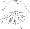
- FIG. 1 shows a molecular beam epitaxy system made in accordance with the present invention.
- Molecular beam epitaxy system 10 includes a molecular beam epitaxy chamber 12 which encloses a substrate 14.
- Molecular beam epitaxy chamber 12 includes an electron gun 16, a phosphorus screen 18 and a flux monitor 20.
- Effusion cells 22, 24, 26, and 28 are carried in molecular beam epitaxy chamber 12.
- effusion cells 22, 24, 26, and 28 may comprise, for example, effusion cells for Zn, Se, and ZnCl 2 .
- the molecular bed epitaxy system 10 includes a free-radical source 30 which is an RF plasma source, in accordance with the present invention.
- Free-radical source 30 may comprise a source of any group VA or oxygen free-radicals.
- free-radical source 30 may provide a source of nitrogen free-radicals, in which free-radical source 30 is supplied with ultra-pure N 2 from an ultra-pure N 2 source 32 through a valve 33.
- RF plasma free-radical source 30 is available from Oxford Applied Research Ltd. (Oxfordshire, UK).
- This free-radical source 30 could include an electron cyclotron resonance (ECR) generator (available from, for example, Wavemat, Inc., 44780 Helm Street, Plymouth, Michigan).
- ECR electron cyclotron resonance
- ZnSe layers were grown on GaAs substrates in a molecular beam epitaxy system in accordance with the present invention. These layers were grown at a substrate temperature of 275°C with a Zn to Se beam equivalent pressure ratio of 1:2 (typical layer thicknesses and growth rates were 2 ⁇ m and 0.5 ⁇ m/h, respectively).
- P-type doping of the ZnSe layers was achieved by a free-radical source which was incorporated in the molecular beam epitaxy system, rather than a conventional effusion source.
- the free-radical source provided a flux of atomic nitrogen (together with a much larger flux of non-dissociated N 2 ) created in a RF plasma discharge chamber.
- a RF frequency of 13.5 MHz was used to generate nitrogen atoms from a gaseous source of ultra-pure N 2 .
- the atomic nitrogen flux level was controlled by suitably adjusting the intensity of the RF plasma discharge.
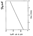
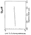
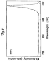
- Net acceptor concentrations, N A -N D , in the nitrogen doped ZnSe/GaAs layers were determined using capacitance-voltage (C-V) profiling. Since the ZnSe epitaxial layers were grown on semi-insulating GaAs, planar profiling between two Schottky contacts on the ZnSe surface was carried out.
- the surface contact pattern consisted of a series of 762 ⁇ m diameter Cr/Au dots physically isolated from a large Cr/Au surrounding electrode. The separation between the inner (dot) electrodes and the outer electrode was 25 ⁇ m, a small separation being necessary in order to maintain a low series resistance.
- the contact pattern was created by thermally evaporating 75 ⁇ of Cr followed by 1000 ⁇ of Au and performing photolithographic and lift-off processes. In all of these measurements the outer electrode was held at ground potential and bias was applied to the inner Schottky contact.
- the doping profile is rather flat from zero bias (0.068 ⁇ m) out to where reverse bias breakdown occurs (1.126 ⁇ m). Breakdown occurred at 3.8 V which is consistent with avalanche breakdown in ZnSe material doped at this level, ie, 3.4x10 17 cm -3 p-type.
- FIG. 4(a) shows a light emitting diode 34.
- Light emitting diode 34 includes a p-type GaAs substrate 36.
- P-type GaAs substrate 36 forms the base for molecular beam epitaxial growth.
- a p-type ZnSe nitrogen doped layer 38 is deposited upon p-type GaAs substrate 36.
- P-type ZnSe layer 38 is deposited in accordance with the present invention using a nitrogen free-radical source.
- An n-type ZnSe chlorine doped layer 40 is deposited upon p-type ZnSe layer 38.
- n + ZnSe cap layer 42 is deposited upon n-type ZnSe layer 40.
- the deposition of layers 38, 40, and 42 is through molecular beam epitaxial growth.
- Ohmic contacts 44 and 46 form electrical contacts to n + ZnSe cap layer 42 and p-type GaAs substrate 36, respectively.
- p-type ZnSe layer 38 has a thickness of 2 ⁇ m and has a net acceptor concentration of 1x10 17 cm -3 .
- N-type ZnSe layer 40 has a thickness of 0.5 ⁇ m and a net donor concentration of 1x10 18 cm -3 .
- the n + ZnSe cap layer 42 has a thickness of 500 ⁇ and a net donor concentration of 5x10 18 cm -3 .
- Figure 4(a) shows the p-type ZnSe layer is grown first on a p + -type GaAs substrate.
- This type of "buried p-type layer" structure avoids the serious problems presently associated with ohmic contact formation to p-type ZnSe (See M.A. Haase, H. Cheng, J.M. DePuydt, and J.E. Potts, J. Appl. Phys., 67, 448 (1990)).
- a disadvantage with this device design is that a large hole barrier exists at the p + -GaAs/p-ZnSe hetero-interface (see L. Kassel, H. Abad, J.W. Garland, P.M.
- Light-emitting diode fabrication was accomplished using conventional photolithographic techniques with device isolation being achieved by wet chemical etching to form 400 ⁇ m diameter mesas.
- the top electrode metalization was ring shaped and was patterned by vacuum evaporation and lift-off. Ultrasonic gold ball bonding was used to make contact to the devices for electroluminescence characterization.
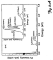
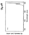
- FIG. 4(b) A typical electroluminescence spectrum recorded at 77K for light emitting diode 34 shown in Figure 4(a), is illustrated in Figure 4(b).
- the device operating voltage and current were 13.5 V and 40 mA, respectively, for the spectrum shown in Figure 4(a).
- the visible electroluminescence is dominated by blue emission, the spectrum comprising a number of resolved lines principally at 447.7 nm, 459.6 nm and 464.7 nm.
- the two highest energy peaks in the spectrum correspond closely in energy to the electroluminescence peaks observed at 77K from blue light-emitting diodes fabricated using a nitrogen-ion implantation and annealing procedure as reported by Akimoto et al (See K.
- Figure 6 shows a light emitting diode 48 made in accordance with the present invention.
- Light emitting diode 48 is a p on n device which operates similar to light emitting diode 34 of Figure 4(a).
- Light emitting diode 48 includes an n + GaAs substrate 50, an n-type ZnSe layer 52 and p-type ZnSe layer 54.
- Contacts 56 and 58 make electrical contact with p-type ZnSe layer 54 and n + GaAs substrate 50.
- the p-type ZnSe layer 54 is deposited using molecular beam epitaxy and a group VA free-radical source in accordance with the present invention.
- diode 48 shown in Figure 6 n-type ZnSe layer 52 has a net donor concentration of about 1x10 18 cm -3 and a thickness of about 2.0 ⁇ m and p-type ZnSe layer 54 has a net acceptor concentration of about 1x10 17 cm -3 and a thickness of 0.5 ⁇ m.
- the present invention provides a method and apparatus for producing conductive p-type IIB-VIA semiconductors films using a free-radical source.
- n-type IIB-VIA semiconductor film may also be produced.
- the resultant IIB-VIA semiconductor film may be used in pn junction devices such as light emitting diodes and light detectors as well as diode lasers and transistors.
- a free-radical source is introduced into a molecular beam epitaxy growth chamber to provide a dopant to a IIB-VIA semiconductor during molecular beam epitaxial growth.
- the free-radical source may be nitrogen, phosphorus, arsenic, and antimony. Oxygen may also be used as a suitable free-radical source.
- the present invention may be used for N-doping and O-doping of ZnSe.
- p-type ternary IIB-VIA semiconductors including Zn 1-x Cd x Se, ZnSe 1-x Te x , ZnSe 1-x S x , ZnS 1-x Te x , and Zn 1-x Cd x S.
- the free-radical source may be a source of any group VA free-radicals, and may provide a dopant for any IIB-VIA semiconductors.
Landscapes
- Engineering & Computer Science (AREA)
- Microelectronics & Electronic Packaging (AREA)
- Physics & Mathematics (AREA)
- Condensed Matter Physics & Semiconductors (AREA)
- General Physics & Mathematics (AREA)
- Manufacturing & Machinery (AREA)
- Computer Hardware Design (AREA)
- Power Engineering (AREA)
- Chemical & Material Sciences (AREA)
- Materials Engineering (AREA)
- Crystallography & Structural Chemistry (AREA)
- Metallurgy (AREA)
- Organic Chemistry (AREA)
- Inorganic Chemistry (AREA)
- Physical Deposition Of Substances That Are Components Of Semiconductor Devices (AREA)
- Led Devices (AREA)
- Semiconductor Lasers (AREA)
Priority Applications (1)
| Application Number | Priority Date | Filing Date | Title |
|---|---|---|---|
| EP04009400A EP1447855A3 (de) | 1990-08-24 | 1991-08-20 | Elektromagnetische Wandler |
Applications Claiming Priority (3)
| Application Number | Priority Date | Filing Date | Title |
|---|---|---|---|
| US07/573,428 US5248631A (en) | 1990-08-24 | 1990-08-24 | Doping of iib-via semiconductors during molecular beam epitaxy using neutral free radicals |
| US573428 | 1990-08-24 | ||
| EP19910307650 EP0475606A3 (en) | 1990-08-24 | 1991-08-20 | Doping of iib-via semiconductors during molecular beam epitaxy |
Related Parent Applications (2)
| Application Number | Title | Priority Date | Filing Date |
|---|---|---|---|
| EP91307650.1 Division | 1991-08-20 | ||
| EP19910307650 Division EP0475606A3 (en) | 1990-08-24 | 1991-08-20 | Doping of iib-via semiconductors during molecular beam epitaxy |
Related Child Applications (1)
| Application Number | Title | Priority Date | Filing Date |
|---|---|---|---|
| EP04009400A Division EP1447855A3 (de) | 1990-08-24 | 1991-08-20 | Elektromagnetische Wandler |
Publications (3)
| Publication Number | Publication Date |
|---|---|
| EP0793281A2 true EP0793281A2 (de) | 1997-09-03 |
| EP0793281A3 EP0793281A3 (de) | 1998-02-04 |
| EP0793281B1 EP0793281B1 (de) | 2005-01-19 |
Family
ID=24291956
Family Applications (3)
| Application Number | Title | Priority Date | Filing Date |
|---|---|---|---|
| EP04009400A Withdrawn EP1447855A3 (de) | 1990-08-24 | 1991-08-20 | Elektromagnetische Wandler |
| EP97106589A Expired - Lifetime EP0793281B1 (de) | 1990-08-24 | 1991-08-20 | Elektromagnetische Umwandler |
| EP19910307650 Ceased EP0475606A3 (en) | 1990-08-24 | 1991-08-20 | Doping of iib-via semiconductors during molecular beam epitaxy |
Family Applications Before (1)
| Application Number | Title | Priority Date | Filing Date |
|---|---|---|---|
| EP04009400A Withdrawn EP1447855A3 (de) | 1990-08-24 | 1991-08-20 | Elektromagnetische Wandler |
Family Applications After (1)
| Application Number | Title | Priority Date | Filing Date |
|---|---|---|---|
| EP19910307650 Ceased EP0475606A3 (en) | 1990-08-24 | 1991-08-20 | Doping of iib-via semiconductors during molecular beam epitaxy |
Country Status (5)
| Country | Link |
|---|---|
| US (2) | US5248631A (de) |
| EP (3) | EP1447855A3 (de) |
| JP (1) | JP3078611B2 (de) |
| KR (1) | KR0156744B1 (de) |
| DE (1) | DE69133443T8 (de) |
Families Citing this family (65)
| Publication number | Priority date | Publication date | Assignee | Title |
|---|---|---|---|---|
| US5633192A (en) * | 1991-03-18 | 1997-05-27 | Boston University | Method for epitaxially growing gallium nitride layers |
| US7235819B2 (en) * | 1991-03-18 | 2007-06-26 | The Trustees Of Boston University | Semiconductor device having group III nitride buffer layer and growth layers |
| WO1992016966A1 (en) * | 1991-03-18 | 1992-10-01 | Boston University | A method for the preparation and doping of highly insulating monocrystalline gallium nitride thin films |
| US5404027A (en) * | 1991-05-15 | 1995-04-04 | Minnesota Mining & Manufacturing Compay | Buried ridge II-VI laser diode |
| CN1111840A (zh) * | 1991-05-15 | 1995-11-15 | 明尼苏达州采矿制造公司 | 蓝-绿激光二极管的制造方法 |
| ES2104931T3 (es) * | 1991-05-15 | 1997-10-16 | Minnesota Mining & Mfg | Diodo de laser azul-verde. |
| US5351255A (en) * | 1992-05-12 | 1994-09-27 | North Carolina State University Of Raleigh | Inverted integrated heterostructure of group II-VI semiconductor materials including epitaxial ohmic contact and method of fabricating same |
| US5818072A (en) * | 1992-05-12 | 1998-10-06 | North Carolina State University | Integrated heterostructure of group II-VI semiconductor materials including epitaxial ohmic contact and method of fabricating same |
| US5541407A (en) * | 1992-09-24 | 1996-07-30 | The United States Of America As Represented By The Secretary Of Commerce | Arsenic atom source |
| US5772759A (en) * | 1992-09-28 | 1998-06-30 | Aixtron Gmbh | Process for producing p-type doped layers, in particular, in II-VI semiconductors |
| US5422902A (en) * | 1993-07-02 | 1995-06-06 | Philips Electronics North America Corporation | BeTe-ZnSe graded band gap ohmic contact to p-type ZnSe semiconductors |
| US5398641A (en) * | 1993-07-27 | 1995-03-21 | Texas Instruments Incorporated | Method for p-type doping of semiconductor structures formed of group II and group VI elements |
| KR960704343A (ko) * | 1994-06-09 | 1996-08-31 | 이데이 노부유키 | 질소도핑 ii-vi족 화합물반도체의 성막방법 |
| JP3410299B2 (ja) * | 1996-08-08 | 2003-05-26 | 科学技術振興事業団 | 高濃度にドーピングしたZnSe結晶の製造方法 |
| US5834330A (en) * | 1996-10-07 | 1998-11-10 | Minnesota Mining And Manufacturing Company | Selective etch method for II-VI semiconductors |
| US5821548A (en) * | 1996-12-20 | 1998-10-13 | Technical Visions, Inc. | Beam source for production of radicals and metastables |
| DE19703615A1 (de) * | 1997-01-31 | 1998-08-06 | Siemens Ag | Optoelektronisches Halbleiterbauelement |
| US6090637A (en) * | 1997-02-13 | 2000-07-18 | 3M Innovative Properties Company | Fabrication of II-VI semiconductor device with BeTe buffer layer |
| US5767534A (en) * | 1997-02-24 | 1998-06-16 | Minnesota Mining And Manufacturing Company | Passivation capping layer for ohmic contact in II-VI semiconductor light transducing device |
| US5963573A (en) * | 1997-08-25 | 1999-10-05 | 3M Innovative Properties Company | Light absorbing layer for II-VI semiconductor light emitting devices |
| US6291085B1 (en) | 1998-08-03 | 2001-09-18 | The Curators Of The University Of Missouri | Zinc oxide films containing P-type dopant and process for preparing same |
| US6342313B1 (en) | 1998-08-03 | 2002-01-29 | The Curators Of The University Of Missouri | Oxide films and process for preparing same |
| TW434844B (en) * | 1999-12-04 | 2001-05-16 | Nat Science Council | Ohmic contact structure of II-VI semiconductor and its fabricating method |
| US6693033B2 (en) * | 2000-02-10 | 2004-02-17 | Motorola, Inc. | Method of removing an amorphous oxide from a monocrystalline surface |
| US6392257B1 (en) | 2000-02-10 | 2002-05-21 | Motorola Inc. | Semiconductor structure, semiconductor device, communicating device, integrated circuit, and process for fabricating the same |
| CN1430792A (zh) | 2000-05-31 | 2003-07-16 | 摩托罗拉公司 | 半导体器件及方法 |
| WO2002009187A2 (en) | 2000-07-24 | 2002-01-31 | Motorola, Inc. | Heterojunction tunneling diodes and process for fabricating same |
| US20020096683A1 (en) | 2001-01-19 | 2002-07-25 | Motorola, Inc. | Structure and method for fabricating GaN devices utilizing the formation of a compliant substrate |
| WO2002082551A1 (en) | 2001-04-02 | 2002-10-17 | Motorola, Inc. | A semiconductor structure exhibiting reduced leakage current |
| US20020195057A1 (en) * | 2001-06-21 | 2002-12-26 | Motorola, Inc. | Apparatus for fabricating semiconductor structures and method of forming the same |
| US6709989B2 (en) | 2001-06-21 | 2004-03-23 | Motorola, Inc. | Method for fabricating a semiconductor structure including a metal oxide interface with silicon |
| US6992321B2 (en) | 2001-07-13 | 2006-01-31 | Motorola, Inc. | Structure and method for fabricating semiconductor structures and devices utilizing piezoelectric materials |
| US7019332B2 (en) | 2001-07-20 | 2006-03-28 | Freescale Semiconductor, Inc. | Fabrication of a wavelength locker within a semiconductor structure |
| US6693298B2 (en) | 2001-07-20 | 2004-02-17 | Motorola, Inc. | Structure and method for fabricating epitaxial semiconductor on insulator (SOI) structures and devices utilizing the formation of a compliant substrate for materials used to form same |
| US6855992B2 (en) | 2001-07-24 | 2005-02-15 | Motorola Inc. | Structure and method for fabricating configurable transistor devices utilizing the formation of a compliant substrate for materials used to form the same |
| US6639249B2 (en) * | 2001-08-06 | 2003-10-28 | Motorola, Inc. | Structure and method for fabrication for a solid-state lighting device |
| US20030026310A1 (en) * | 2001-08-06 | 2003-02-06 | Motorola, Inc. | Structure and method for fabrication for a lighting device |
| US20030034491A1 (en) | 2001-08-14 | 2003-02-20 | Motorola, Inc. | Structure and method for fabricating semiconductor structures and devices for detecting an object |
| US6673667B2 (en) * | 2001-08-15 | 2004-01-06 | Motorola, Inc. | Method for manufacturing a substantially integral monolithic apparatus including a plurality of semiconductor materials |
| CA2396325C (en) * | 2001-09-06 | 2010-03-30 | Sumitomo Electric Industries, Ltd. | Zn1-xmgxsyse1-y pin photodiode and zn1-xmgxsyse1-y avalanche-photodiode |
| US20030071327A1 (en) | 2001-10-17 | 2003-04-17 | Motorola, Inc. | Method and apparatus utilizing monocrystalline insulator |
| US6727524B2 (en) * | 2002-03-22 | 2004-04-27 | Kulite Semiconductor Products, Inc. | P-n junction structure |
| US6916717B2 (en) | 2002-05-03 | 2005-07-12 | Motorola, Inc. | Method for growing a monocrystalline oxide layer and for fabricating a semiconductor device on a monocrystalline substrate |
| US6887736B2 (en) * | 2002-06-24 | 2005-05-03 | Cermet, Inc. | Method of forming a p-type group II-VI semiconductor crystal layer on a substrate |
| US7169619B2 (en) * | 2002-11-19 | 2007-01-30 | Freescale Semiconductor, Inc. | Method for fabricating semiconductor structures on vicinal substrates using a low temperature, low pressure, alkaline earth metal-rich process |
| US6885065B2 (en) | 2002-11-20 | 2005-04-26 | Freescale Semiconductor, Inc. | Ferromagnetic semiconductor structure and method for forming the same |
| US6806202B2 (en) | 2002-12-03 | 2004-10-19 | Motorola, Inc. | Method of removing silicon oxide from a surface of a substrate |
| US6963090B2 (en) | 2003-01-09 | 2005-11-08 | Freescale Semiconductor, Inc. | Enhancement mode metal-oxide-semiconductor field effect transistor |
| US6965128B2 (en) | 2003-02-03 | 2005-11-15 | Freescale Semiconductor, Inc. | Structure and method for fabricating semiconductor microresonator devices |
| US7612432B2 (en) | 2004-02-06 | 2009-11-03 | Hoya Corporation | P-type ZnS based semiconductor material having a low resistance due to its high copper content |
| US20060049425A1 (en) * | 2004-05-14 | 2006-03-09 | Cermet, Inc. | Zinc-oxide-based light-emitting diode |
| US20070111372A1 (en) * | 2004-07-20 | 2007-05-17 | Cermet, Inc. | Methods of forming a p-type group ii-vi semiconductor crystal layer on a substrate |
| US7723154B1 (en) | 2005-10-19 | 2010-05-25 | North Carolina State University | Methods of forming zinc oxide based II-VI compound semiconductor layers with shallow acceptor conductivities |
| JP4832250B2 (ja) * | 2006-10-23 | 2011-12-07 | Hoya株式会社 | p型半導体材料、半導体素子、有機エレクトロルミネッセンス素子、及びp型半導体材料の製造方法 |
| TW200949004A (en) * | 2008-04-25 | 2009-12-01 | Lumenz Inc | Metalorganic chemical vapor deposition of zinc oxide |
| CA2744774C (en) | 2008-07-17 | 2017-05-23 | Uriel Solar, Inc. | High power efficiency, large substrate, polycrystalline cdte thin film semiconductor photovoltaic cell structures grown by molecular beam epitaxy at high deposition rate for use in solar electricity generation |
| CN102804411A (zh) * | 2009-05-05 | 2012-11-28 | 3M创新有限公司 | 利用铟耗尽机理在含铟衬底上生长的半导体器件 |
| US20110139249A1 (en) * | 2009-12-10 | 2011-06-16 | Uriel Solar Inc. | High Power Efficiency Polycrystalline CdTe Thin Film Semiconductor Photovoltaic Cell Structures for Use in Solar Electricity Generation |
| US7829376B1 (en) | 2010-04-07 | 2010-11-09 | Lumenz, Inc. | Methods of forming zinc oxide based II-VI compound semiconductor layers with shallow acceptor conductivities |
| CN103597614B (zh) | 2011-06-15 | 2017-03-01 | 3M创新有限公司 | 具有改善的转换效率的太阳能电池 |
| RU2511279C1 (ru) * | 2012-10-22 | 2014-04-10 | Федеральное Государственное Бюджетное Образовательное Учреждение Высшего Профессионального Образования "Нижегородский Государственный Университет Им. Н.И. Лобачевского" | Способ напыления в вакууме структур для приборов электронной техники, способ регулирования концентрации легирующих примесей при выращивании таких структур и резистивный источник паров напыляемого материала и легирующей примеси для реализации указанного способа регулирования, а также основанный на использовании этого источника паров способ напыления в вакууме кремний-германиевых структур |
| US20150053259A1 (en) * | 2013-08-22 | 2015-02-26 | Plant PV | P-type doping of ii-vi materials with rapid vapor deposition using radical nitrogen |
| KR102657362B1 (ko) | 2015-06-16 | 2024-04-16 | 조지아 테크 리서치 코포레이션 | Iii족 질화물 반도체 성장 속도를 증가 및 이온 플럭스 훼손의 감소를 위한 시스템 및 방법 |
| WO2019103459A2 (ko) | 2017-11-22 | 2019-05-31 | 주식회사 엘지화학 | 리튬 이차전지용 양극 첨가제의 제조방법 |
| RU2699949C1 (ru) * | 2019-02-08 | 2019-09-11 | Федеральное государственное автономное образовательное учреждение высшего образования "Национальный исследовательский Нижегородский государственный университет им. Н.И. Лобачевского" | Способ настройки эпитаксиального выращивания в вакууме легированных слоёв кремния и резистивный испарительный блок для его осуществления |
Family Cites Families (18)
| Publication number | Priority date | Publication date | Assignee | Title |
|---|---|---|---|---|
| US3735212A (en) * | 1971-02-25 | 1973-05-22 | Zenith Radio Corp | P-n junction semiconductor devices |
| US3745073A (en) * | 1971-02-26 | 1973-07-10 | Zenith Radio Corp | Single-step process for making p-n junctions in zinc selenide |
| US4081764A (en) * | 1972-10-12 | 1978-03-28 | Minnesota Mining And Manufacturing Company | Zinc oxide light emitting diode |
| US4483725A (en) * | 1982-09-30 | 1984-11-20 | At&T Bell Laboratories | Reactive vapor deposition of multiconstituent material |
| JPS61117199A (ja) * | 1984-11-08 | 1986-06-04 | Nec Corp | 結晶成長法 |
| JPH0621036B2 (ja) * | 1984-11-09 | 1994-03-23 | 大塚化学株式会社 | 導電性チタン酸塩誘導体及びその製造法 |
| US4735910A (en) * | 1985-09-19 | 1988-04-05 | Matsushita Electric Industrial Co., Ltd. | In-situ doping of MBE grown II-VI compounds on a homo- or hetero-substrate |
| JPH07105342B2 (ja) * | 1986-01-17 | 1995-11-13 | 三洋電機株式会社 | 化合物半導体の製造方法 |
| JPH0728052B2 (ja) * | 1986-01-27 | 1995-03-29 | 株式会社東芝 | 半導体発光素子およびその製造方法 |
| JPH0617280B2 (ja) * | 1987-03-18 | 1994-03-09 | 社団法人生産技術振興協会 | ZnSe単結晶作製法 |
| JPH0728097B2 (ja) * | 1987-05-20 | 1995-03-29 | 松下電器産業株式会社 | 半導体レ−ザ |
| JPH06104600B2 (ja) * | 1987-05-30 | 1994-12-21 | 松下電器産業株式会社 | 半導体の製造方法 |
| JPH07517B2 (ja) * | 1987-05-30 | 1995-01-11 | 松下電器産業株式会社 | 半導体結晶薄膜製造装置 |
| JPH01232651A (ja) * | 1988-03-11 | 1989-09-18 | Hitachi Ltd | ラジカルビーム発生装置 |
| JP2712257B2 (ja) * | 1988-03-30 | 1998-02-10 | ソニー株式会社 | セレン化亜鉛の成長方法 |
| JPH02262380A (ja) * | 1989-04-03 | 1990-10-25 | Toshiba Corp | 半導体発光素子 |
| JP2588280B2 (ja) * | 1989-07-10 | 1997-03-05 | シャープ株式会社 | 化合物半導体発光素子 |
| US5150191A (en) * | 1989-11-21 | 1992-09-22 | Kabushiki Kaisha Toshiba | P-type II-VI compound semiconductor doped |
-
1990
- 1990-08-24 US US07/573,428 patent/US5248631A/en not_active Expired - Lifetime
-
1991
- 1991-08-20 EP EP04009400A patent/EP1447855A3/de not_active Withdrawn
- 1991-08-20 EP EP97106589A patent/EP0793281B1/de not_active Expired - Lifetime
- 1991-08-20 DE DE69133443T patent/DE69133443T8/de active Active
- 1991-08-20 EP EP19910307650 patent/EP0475606A3/en not_active Ceased
- 1991-08-22 KR KR1019910014478A patent/KR0156744B1/ko not_active Expired - Fee Related
- 1991-08-23 JP JP03212195A patent/JP3078611B2/ja not_active Expired - Fee Related
-
1993
- 1993-07-21 US US08/095,872 patent/US5574296A/en not_active Expired - Lifetime
Also Published As
| Publication number | Publication date |
|---|---|
| US5248631A (en) | 1993-09-28 |
| EP0475606A3 (en) | 1992-06-17 |
| EP1447855A3 (de) | 2004-12-29 |
| DE69133443D1 (de) | 2005-02-24 |
| EP1447855A2 (de) | 2004-08-18 |
| DE69133443T8 (de) | 2006-04-27 |
| JP3078611B2 (ja) | 2000-08-21 |
| US5574296A (en) | 1996-11-12 |
| HK1002373A1 (en) | 1998-08-21 |
| EP0475606A2 (de) | 1992-03-18 |
| EP0793281B1 (de) | 2005-01-19 |
| DE69133443T2 (de) | 2006-02-09 |
| KR920005258A (ko) | 1992-03-28 |
| JPH04234136A (ja) | 1992-08-21 |
| EP0793281A3 (de) | 1998-02-04 |
| KR0156744B1 (ko) | 1998-12-01 |
Similar Documents
| Publication | Publication Date | Title |
|---|---|---|
| EP0793281B1 (de) | Elektromagnetische Umwandler | |
| Park et al. | p‐type ZnSe by nitrogen atom beam doping during molecular beam epitaxial growth | |
| EP0584236B1 (de) | Blau-gruen diodenlaser | |
| US5818072A (en) | Integrated heterostructure of group II-VI semiconductor materials including epitaxial ohmic contact and method of fabricating same | |
| US5291507A (en) | Blue-green laser diode | |
| Morkoc et al. | Large‐band‐gap SiC, III‐V nitride, and II‐VI ZnSe‐based semiconductor device technologies | |
| US7622398B2 (en) | Semiconductor device, semiconductor layer and production method thereof | |
| EP0640248B1 (de) | Epitaktischer ohmscher Kontakt für integrierte Heterostruktur von II-VI-Halbleitermaterialien und Verfahren zu seiner Herstellung | |
| HK1001353B (en) | Blue-green laser diode | |
| US5274269A (en) | Ohmic contact for p-type group II-IV compound semiconductors | |
| Kondo et al. | InGaP orange light‐emitting diodes on Si substrates | |
| KR100343849B1 (ko) | 에피택시얼웨이퍼및이의제조방법과휘도가증가된발광다이오드 | |
| EP0350058B1 (de) | Herstellungsverfahren einer grünes Licht emittierenden Diode | |
| HK1002373B (en) | Electro-magnetic transducers | |
| RU2151457C1 (ru) | Способ изготовления омического контактного слоя и полупроводниковое устройство ii-vi групп | |
| JP2999591B2 (ja) | 高純度の真性層を有するGaAs素子の製造方法 | |
| Grillo et al. | MBE growth and microstructural evaluation of Zn (S, Se)-based LEDs and diode lasers | |
| Wu et al. | Status of II–VI molecular-beam epitaxy technology | |
| Park | ZnSe growth by conventional molecular beam epitaxy: a review of recent progress | |
| Hishida et al. | Molecular beam epitaxy of p‐type conducting ZnSe and ZnSSe by simple nitrogen gas doping without plasma activation | |
| Cortes | Molecular-Beam Epitaxy of HgCdTe for Electro-Optical Infrared Applications |
Legal Events
| Date | Code | Title | Description |
|---|---|---|---|
| PUAI | Public reference made under article 153(3) epc to a published international application that has entered the european phase |
Free format text: ORIGINAL CODE: 0009012 |
|
| AC | Divisional application: reference to earlier application |
Ref document number: 475606 Country of ref document: EP |
|
| AK | Designated contracting states |
Kind code of ref document: A2 Designated state(s): DE FR GB NL |
|
| RIN1 | Information on inventor provided before grant (corrected) |
Inventor name: CHENG, HWA Inventor name: DEPUYDT, JAMES M. Inventor name: PARK, ROBERT M. |
|
| PUAL | Search report despatched |
Free format text: ORIGINAL CODE: 0009013 |
|
| AK | Designated contracting states |
Kind code of ref document: A3 Designated state(s): DE FR GB NL |
|
| 17P | Request for examination filed |
Effective date: 19980720 |
|
| 17Q | First examination report despatched |
Effective date: 19990622 |
|
| APAB | Appeal dossier modified |
Free format text: ORIGINAL CODE: EPIDOS NOAPE |
|
| APAB | Appeal dossier modified |
Free format text: ORIGINAL CODE: EPIDOS NOAPE |
|
| APAD | Appeal reference recorded |
Free format text: ORIGINAL CODE: EPIDOS REFNE |
|
| APBT | Appeal procedure closed |
Free format text: ORIGINAL CODE: EPIDOSNNOA9E |
|
| APBT | Appeal procedure closed |
Free format text: ORIGINAL CODE: EPIDOSNNOA9E |
|
| APBV | Interlocutory revision of appeal recorded |
Free format text: ORIGINAL CODE: EPIDOSNIRAPE |
|
| APBD | Information on interlocutory revision deleted |
Free format text: ORIGINAL CODE: EPIDOSDIRAPE |
|
| GRAP | Despatch of communication of intention to grant a patent |
Free format text: ORIGINAL CODE: EPIDOSNIGR1 |
|
| GRAS | Grant fee paid |
Free format text: ORIGINAL CODE: EPIDOSNIGR3 |
|
| GRAA | (expected) grant |
Free format text: ORIGINAL CODE: 0009210 |
|
| AC | Divisional application: reference to earlier application |
Ref document number: 0475606 Country of ref document: EP Kind code of ref document: P |
|
| AK | Designated contracting states |
Kind code of ref document: B1 Designated state(s): DE FR GB NL |
|
| REG | Reference to a national code |
Ref country code: GB Ref legal event code: FG4D |
|
| REF | Corresponds to: |
Ref document number: 69133443 Country of ref document: DE Date of ref document: 20050224 Kind code of ref document: P |
|
| REG | Reference to a national code |
Ref country code: HK Ref legal event code: GR Ref document number: 1002373 Country of ref document: HK |
|
| APAH | Appeal reference modified |
Free format text: ORIGINAL CODE: EPIDOSCREFNO |
|
| PLBE | No opposition filed within time limit |
Free format text: ORIGINAL CODE: 0009261 |
|
| STAA | Information on the status of an ep patent application or granted ep patent |
Free format text: STATUS: NO OPPOSITION FILED WITHIN TIME LIMIT |
|
| ET | Fr: translation filed | ||
| 26N | No opposition filed |
Effective date: 20051020 |
|
| PGFP | Annual fee paid to national office [announced via postgrant information from national office to epo] |
Ref country code: NL Payment date: 20060824 Year of fee payment: 16 |
|
| PGFP | Annual fee paid to national office [announced via postgrant information from national office to epo] |
Ref country code: FR Payment date: 20060831 Year of fee payment: 16 |
|
| PGFP | Annual fee paid to national office [announced via postgrant information from national office to epo] |
Ref country code: GB Payment date: 20070830 Year of fee payment: 17 |
|
| PG25 | Lapsed in a contracting state [announced via postgrant information from national office to epo] |
Ref country code: NL Free format text: LAPSE BECAUSE OF NON-PAYMENT OF DUE FEES Effective date: 20080301 |
|
| NLV4 | Nl: lapsed or anulled due to non-payment of the annual fee |
Effective date: 20080301 |
|
| REG | Reference to a national code |
Ref country code: FR Ref legal event code: ST Effective date: 20080430 |
|
| PG25 | Lapsed in a contracting state [announced via postgrant information from national office to epo] |
Ref country code: FR Free format text: LAPSE BECAUSE OF NON-PAYMENT OF DUE FEES Effective date: 20070831 |
|
| GBPC | Gb: european patent ceased through non-payment of renewal fee |
Effective date: 20080820 |
|
| PG25 | Lapsed in a contracting state [announced via postgrant information from national office to epo] |
Ref country code: GB Free format text: LAPSE BECAUSE OF NON-PAYMENT OF DUE FEES Effective date: 20080820 |
|
| PGFP | Annual fee paid to national office [announced via postgrant information from national office to epo] |
Ref country code: DE Payment date: 20090827 Year of fee payment: 19 |
|
| REG | Reference to a national code |
Ref country code: DE Ref legal event code: R119 Ref document number: 69133443 Country of ref document: DE Effective date: 20110301 |
|
| PG25 | Lapsed in a contracting state [announced via postgrant information from national office to epo] |
Ref country code: DE Free format text: LAPSE BECAUSE OF NON-PAYMENT OF DUE FEES Effective date: 20110301 |