EP0789397A2 - Schaltungsplatine und Halbleiterbauteil mit dieser - Google Patents
Schaltungsplatine und Halbleiterbauteil mit dieser Download PDFInfo
- Publication number
- EP0789397A2 EP0789397A2 EP97300625A EP97300625A EP0789397A2 EP 0789397 A2 EP0789397 A2 EP 0789397A2 EP 97300625 A EP97300625 A EP 97300625A EP 97300625 A EP97300625 A EP 97300625A EP 0789397 A2 EP0789397 A2 EP 0789397A2
- Authority
- EP
- European Patent Office
- Prior art keywords
- conductive foil
- bonding layer
- insulating substrate
- edges
- pattern
- Prior art date
- Legal status (The legal status is an assumption and is not a legal conclusion. Google has not performed a legal analysis and makes no representation as to the accuracy of the status listed.)
- Granted
Links
Images


Classifications
-
- H—ELECTRICITY
- H05—ELECTRIC TECHNIQUES NOT OTHERWISE PROVIDED FOR
- H05K—PRINTED CIRCUITS; CASINGS OR CONSTRUCTIONAL DETAILS OF ELECTRIC APPARATUS; MANUFACTURE OF ASSEMBLAGES OF ELECTRICAL COMPONENTS
- H05K1/00—Printed circuits
- H05K1/02—Details
- H05K1/0271—Arrangements for reducing stress or warp in rigid printed circuit boards, e.g. caused by loads, vibrations or differences in thermal expansion
-
- H—ELECTRICITY
- H10—SEMICONDUCTOR DEVICES; ELECTRIC SOLID-STATE DEVICES NOT OTHERWISE PROVIDED FOR
- H10W—GENERIC PACKAGES, INTERCONNECTIONS, CONNECTORS OR OTHER CONSTRUCTIONAL DETAILS OF DEVICES COVERED BY CLASS H10
- H10W40/00—Arrangements for thermal protection or thermal control
- H10W40/20—Arrangements for cooling
- H10W40/25—Arrangements for cooling characterised by their materials
- H10W40/255—Arrangements for cooling characterised by their materials having a laminate or multilayered structure, e.g. direct bond copper [DBC] ceramic substrates
-
- H—ELECTRICITY
- H10—SEMICONDUCTOR DEVICES; ELECTRIC SOLID-STATE DEVICES NOT OTHERWISE PROVIDED FOR
- H10W—GENERIC PACKAGES, INTERCONNECTIONS, CONNECTORS OR OTHER CONSTRUCTIONAL DETAILS OF DEVICES COVERED BY CLASS H10
- H10W70/00—Package substrates; Interposers; Redistribution layers [RDL]
- H10W70/60—Insulating or insulated package substrates; Interposers; Redistribution layers
- H10W70/67—Insulating or insulated package substrates; Interposers; Redistribution layers characterised by their insulating layers or insulating parts
- H10W70/68—Shapes or dispositions thereof
-
- H—ELECTRICITY
- H05—ELECTRIC TECHNIQUES NOT OTHERWISE PROVIDED FOR
- H05K—PRINTED CIRCUITS; CASINGS OR CONSTRUCTIONAL DETAILS OF ELECTRIC APPARATUS; MANUFACTURE OF ASSEMBLAGES OF ELECTRICAL COMPONENTS
- H05K1/00—Printed circuits
- H05K1/02—Details
- H05K1/03—Use of materials for the substrate
- H05K1/0306—Inorganic insulating substrates, e.g. ceramic, glass
-
- H—ELECTRICITY
- H05—ELECTRIC TECHNIQUES NOT OTHERWISE PROVIDED FOR
- H05K—PRINTED CIRCUITS; CASINGS OR CONSTRUCTIONAL DETAILS OF ELECTRIC APPARATUS; MANUFACTURE OF ASSEMBLAGES OF ELECTRICAL COMPONENTS
- H05K2201/00—Indexing scheme relating to printed circuits covered by H05K1/00
- H05K2201/09—Shape and layout
- H05K2201/09145—Edge details
-
- H—ELECTRICITY
- H05—ELECTRIC TECHNIQUES NOT OTHERWISE PROVIDED FOR
- H05K—PRINTED CIRCUITS; CASINGS OR CONSTRUCTIONAL DETAILS OF ELECTRIC APPARATUS; MANUFACTURE OF ASSEMBLAGES OF ELECTRICAL COMPONENTS
- H05K2201/00—Indexing scheme relating to printed circuits covered by H05K1/00
- H05K2201/09—Shape and layout
- H05K2201/09209—Shape and layout details of conductors
- H05K2201/09654—Shape and layout details of conductors covering at least two types of conductors provided for in H05K2201/09218 - H05K2201/095
- H05K2201/098—Special shape of the cross-section of conductors, e.g. very thick plated conductors
-
- H—ELECTRICITY
- H05—ELECTRIC TECHNIQUES NOT OTHERWISE PROVIDED FOR
- H05K—PRINTED CIRCUITS; CASINGS OR CONSTRUCTIONAL DETAILS OF ELECTRIC APPARATUS; MANUFACTURE OF ASSEMBLAGES OF ELECTRICAL COMPONENTS
- H05K3/00—Apparatus or processes for manufacturing printed circuits
- H05K3/0058—Laminating printed circuit boards onto other substrates, e.g. metallic substrates
-
- H—ELECTRICITY
- H05—ELECTRIC TECHNIQUES NOT OTHERWISE PROVIDED FOR
- H05K—PRINTED CIRCUITS; CASINGS OR CONSTRUCTIONAL DETAILS OF ELECTRIC APPARATUS; MANUFACTURE OF ASSEMBLAGES OF ELECTRICAL COMPONENTS
- H05K3/00—Apparatus or processes for manufacturing printed circuits
- H05K3/38—Improvement of the adhesion between the insulating substrate and the metal
-
- H—ELECTRICITY
- H10—SEMICONDUCTOR DEVICES; ELECTRIC SOLID-STATE DEVICES NOT OTHERWISE PROVIDED FOR
- H10W—GENERIC PACKAGES, INTERCONNECTIONS, CONNECTORS OR OTHER CONSTRUCTIONAL DETAILS OF DEVICES COVERED BY CLASS H10
- H10W72/00—Interconnections or connectors in packages
- H10W72/851—Dispositions of multiple connectors or interconnections
- H10W72/874—On different surfaces
- H10W72/884—Die-attach connectors and bond wires
-
- H—ELECTRICITY
- H10—SEMICONDUCTOR DEVICES; ELECTRIC SOLID-STATE DEVICES NOT OTHERWISE PROVIDED FOR
- H10W—GENERIC PACKAGES, INTERCONNECTIONS, CONNECTORS OR OTHER CONSTRUCTIONAL DETAILS OF DEVICES COVERED BY CLASS H10
- H10W90/00—Package configurations
- H10W90/701—Package configurations characterised by the relative positions of pads or connectors relative to package parts
- H10W90/731—Package configurations characterised by the relative positions of pads or connectors relative to package parts of die-attach connectors
- H10W90/734—Package configurations characterised by the relative positions of pads or connectors relative to package parts of die-attach connectors between a chip and a stacked insulating package substrate, interposer or RDL
-
- H—ELECTRICITY
- H10—SEMICONDUCTOR DEVICES; ELECTRIC SOLID-STATE DEVICES NOT OTHERWISE PROVIDED FOR
- H10W—GENERIC PACKAGES, INTERCONNECTIONS, CONNECTORS OR OTHER CONSTRUCTIONAL DETAILS OF DEVICES COVERED BY CLASS H10
- H10W90/00—Package configurations
- H10W90/701—Package configurations characterised by the relative positions of pads or connectors relative to package parts
- H10W90/751—Package configurations characterised by the relative positions of pads or connectors relative to package parts of bond wires
- H10W90/754—Package configurations characterised by the relative positions of pads or connectors relative to package parts of bond wires between a chip and a stacked insulating package substrate, interposer or RDL
Definitions
- the present invention relates to a technique of mounting a power semiconductor device and, more specifically, to a semiconductor device of a module structure including an insulating substrate with a conductive foil bonded thereto.
- a power semiconductor element 4 is bonded with solder 6 to a circuit board having an insulating substrate 1 provided with a wiring pattern of a conductive foil 3, and the circuit board is bonded to a metal base plate 8 of molybdenum or copper with solder 7.
- the insulating substrate 1 is a ceramic substrate of aluminum oxide, aluminum nitride or the like.
- a copper foil formed in a circuit pattern is bonded to the ceramic substrate by, for example, an active metal method disclosed in JP-A No. 60-177634 using a silver solder, or a method disclosed in JP-A No. 56-163093 which bonds a copper foil directly to an aluminum nitride substrate.
- the active metal method bonds a copper foil to an insulating substrate at a temperature lower than that at which the method bonds a copper foil to a substrate. Therefore, a residual stress induced within a structure formed by bonding a copper foil to an aluminum nitride insulating substrate by the active metal method due to the difference in coefficient of thermal expansion between the aluminum nitride insulating substrate and the copper foil is relatively small, and hence the structure is durable to thermal load that is exerted thereon by, for example, heat cycle.
- Heat generated by the semiconductor element 4 is transferred through the circuit pattern of the conductive foil 3, the insulating substrate 1, the metal base plate 8 of molybdenum or copper and a grease layer 9 to a heat sink 10 which radiates heat.
- the temperatures of the insulating substrate 1 provided with the pattern of the conductive foil 3 , and the metal base plate 8, i.e., the components of the module, are elevated while the semiconductor element 4 is in operation.
- the temperatures of those components drop down after the operation of the semiconductor element 4 is stopped.
- the temperatures of the components of the module rise and drop repeatedly. Consequently, thermal stress is induced in the insulating substrate 1 due to difference in coefficient of thermal expansion between the insulating substrate 1 and the circuit pattern of the conductive foil 3 and, in some cases,
- the present invention provides a highly reliable circuit board and a highly reliable semiconductor device of a module structure including a power semiconductor element and an insulating substrate, capable of preventing the development of cracks in the insulating substrate.
- a semiconductor device comprises a metal base plate, an insulating substrate placed on the metal base plate, a conductive foil bonded to the insulating substrate with a bonding layer, and a semiconductor element mounted on the conductive foil.
- a marginal portion of the bonding layer spreads outside beyond the edges of the conductive foil, the marginal portion of the bonding layer spreading outside beyond the edges of the conductive foil has a width greater than the thickness of the bonding layer, and the thickness of the marginal portion of the bonding layer spreading outside beyond the edges of the conductive foil is 0.1 mm or below.
- a semiconductor device comprises a metal base plate, an insulating substrate placed on the metal base plate, a conductive foil bonded to the insulating substrate with a bonding layer, and a semiconductor element mounted on the conductive foil.
- the bonding layer has an area greater than that of the conductive foil, the marginal portion of the bonding layer spreading outside beyond the edges of the conductive foil has a width greater than the thickness of the bonding layer, and the thickness of the marginal portion of the bonding layer spreading outside beyond the edges of the conductive foil is 0.1 mm or below.
- a semiconductor device comprises a metal base plate, an insulating substrate placed on the metal base plate, a conductive foil bonded to the insulating substrate with a bonding layer, and a semiconductor element mounted on the conductive foil.
- Edges of corner portions of a pattern of the bonding layer lie outside corresponding edges of corner portions of the pattern of the conductive foil, the width of the largest corner portion of the pattern of the bonding layer lying outside the edges of the corresponding corner portion of the pattern of the conductive foil is greater than the thickness of the bonding layer, and the thickness of the largest corner portion of the pattern of the bonding layer lying outside the edges of the corresponding corner portion of the pattern of the conductive foil is 0.1 mm or below.
- a semiconductor device comprises a metal base plate, an insulating substrate placed on the metal base plate, a conductive foil bonded to the insulating substrate with a bonding layer, and a semiconductor element mounted on the conductive foil.
- a marginal portion of the bonding layer spreads outside beyond the edges of the conductive foil, the conductive foil is bonded to the insulating substrate with a plurality of kinds of bonding layers, and a plurality of kinds of bonding layers the same as those bonding the conductive foil to the insulating substrate are formed on the conductive foil.
- a circuit board includes the insulating substrate and the conduclive foil.
- a volume of the conductive foil on the marginal portion of the bonding layer is zero. Therfor, a thermal stress in a portion of the insulating substrate bonded to the marginal portion of the bonding layer is reduced.
- Fig. 1 is a typical sectional view of a module embodying the present invention.
- Figs. 2(a) and 2(b) are a plan view and a sectional view, respectively, of an embodiment of the present invention.
- Fig. 3 is a plan view of an embodiment of the present invention.
- Fig. 4 is a typical sectional view of a conventional module.
- Fig. 5 is a graph showing the dependence of the number of heat cycles at which cracks developed in the insulating substrate on the width of the marginal portion spreading outside beyond the edges of the circuit pattern of the conductive foil.
- Figs. 6(a) and 6(b) are a sectional view and a plan view, respectively, of an embodiment of the present invention.
- Figs. 7(a) and 7(b) are a sectional view and a plan view, respectively, of an embodiment of the present invention.
- Figs. 8(a) and 8(b) are a sectional view and a plan view, respectively, of an embodiment of the present invention.
- Figs. 9(a) and 9(b) are a sectional view and a plan view, respectively, of an embodiment of the present invention.
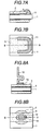
- Figs. 10(a) and 10(b) are a sectional view of edge of a circuit board of an embodiment of the present invention.
- a conventional method fabricates an insulating substrate 1 provided with a circuit pattern 3 of a conductive foil by printing a bonding layer 2 in a pattern corresponding to the circuit pattern 3 on the insulating substrate 1, spreading a copper foil over the printed bonding layer 2, applying a pressure to the copper foil to bond the copper foil to the insulating substrate 1, etching the copper foil to form the circuit pattern 3 of the conductive foil.
- the bonding layer 2 is formed in a shape identical with the circuit pattern 3 of the conductive foil , i.e., the copper foil.
- the conductive foil forming the circuit pattern 3 is a copper foil
- the insulating substrate 1 is made of a ceramic material.
- the coefficient of thermal expansion of copper is 17 ⁇ 10 -6 °C
- those of aluminum oxide and aluminum nitride are 6.5 ⁇ 10 -6 /°C and 4.5 ⁇ 10 -6 /°C , respectively. Therefore, a maximum stress is induced in a portion of the ceramic substrate corresponding to a marginal portion 14 of the circuit pattern 3 of the conductive foil due to difference in coefficient of thermal expansion between the conductive foil forming the circuit pattern 3 and the insulating substrate 1.
- the bonding layer 2 is formed in a pattern having a marginal portion 15 lying within the marginal portion 14 of the circuit pattern due to insufficient accuracy in the alignment of an etching mask for forming the circuit pattern and a printing mask for printing the bonding layer, an increased stress is concentrated on a portion of the ceramic substrate corresponding to the marginal portion 15 and thereby cracks are liable to be formed in the ceramic substrate.
- the stress induced in the ceramic substrate increases with the increase of the thickness of the conductive foil forming the circuit pattern 3.
- a method disclosed in JP-A No. 5-152461 forms the marginal portion 14 of the circuit pattern of the conductive foil in a reduced thickness by a mechanical means, such as a press, or a chemical means, such as etching.
- the present invention solves the problem by forming the bonding layer 2 in an area greater than that of the circuit pattern 3 of the conductive foil. Since the edges of the marginal portion 15 of the bonding layer 2 is not true with those of the marginal portion 14 of the circuit pattern 3 of the conductive foil, stress concentration on a particular portion of the ceramic substrate is alleviated regardless of the thickness of the conductive foil forming the circuit pattern 3.
- Fig. 2(a) is a plan view of an insulating substrate 1 provided with circuit pattern 3 of a conductive foil
- Figs. 2(b) is a sectional view taken on line A-A in Fig. 2(a).
- the insulating substrate 1 was an aluminum nitride substrate.
- the insulating substrate 1 may be a substrate of any suitable electrically insulating material, such as formed of a ceramic material other than aluminum nitride, such as aluminum oxide or silicon carbide, of a composite material formed by laminating a metal substrate and a ceramic substrate.
- a bonding layer 2 was formed by spreading a silver solder containing silver and copper as principal components.
- the silver solder contains a metal having a coefficient of thermal expansion between those of the material of the conductive foils forming the circuit patterns 3 and the material of the ceramic substrate to reduce adverse effects attributable to the difference in coefficient of thermal expansion between the circuit patterns 3 and the ceramic substrate.
- titanium hydride is added to the silver solder to enhance the bonding strength between the silver solder and the aluminum nitride substrate.
- the circuit patterns 3 were formed by processing rolled copper foils.
- the insulating substrate 1 provided with the circuit patterns 3 of the conductive foils was fabricated by the following method.
- bonding layers 2 of the silver solder were formed in predetermined patterns over the opposite surfaces of the aluminum nitride substrate, respectively, by screen printing, and the bonding layers 2 were dried. Subsequently, copper foils were spread over and in close contact with the opposite surfaces of the aluminum nitride substrate on which the bonding layers 2 are formed, respectively, and pressure and heat were applied through spacers to the copper foils to obtain the insulating substrate with the copper foils bonded thereto. Then, the insulating substrate with the copper foils bonded thereto was subjected to an etching process to form the circuit patterns 3 of the conductive foils.
- resist patterns were formed so that the edges of the circuit patterns formed by etching the copper foils lie within the patterns of bonding layers of the silver solder. As shown in Fig. 2(a), the patterns of the bonding layers 2 thus formed have areas greater than those of the corresponding circuit patterns 3 of the conductive foils, respectively.
- the surfaces of the circuit patterns 3 of the conductive foils, i.e., the copper foils, formed on the insulating substrate 1 were coated with an antioxidation films by an electroless nickel-phosphorus plating process.
- Table 1 shows the results of -40° C /125° C heat cycle tests of modules of different structures conducted to evaluate the heat cycle reliability of the modules.
- Test module 3 provided with the silver solder layer having an area greater than that of the corresponding copper foil, no crack developed in the insulating substrate 1, the copper foil did not come off the insulating substrate 1 and the module functioned normally after 1000 heat cycles.
- Test module 2 provided with the silver solder layer having an area and a shape the same as those of the copper foil, cracks developed in the insulating substrate 1 and the copper foil came off the insulating substrate after 200 heat cycles.
- Test module 1 provided with the silver solder layer of an area and a shape smaller than those of the copper foil, cracks developed in the insulating substrate 1 and the copper foil came off the insulating substrate 1 after 50 heat cycles.
- Fig. 3 is a plan view of a circuit pattern 3 of a conductive foil employed in the third embodiment. It is preferable that the circuit pattern 3 of the conductive foil has a large area to carry a high current. Therefore, the straight edges of a circuit pattern 3 were formed so as to be true with the corresponding edges of a pattern of a bonding layer 2, and the corners of the circuit pattern 3 of the conductive foil were rounded in shapes of a radius of curvature greater than that of the corresponding corners of the pattern of the bonding layer 2. Thus, the corner portions of the pattern of the bonding layer 2 spread outside beyond the corresponding edges of the circuit pattern 3.
- the module in the third embodiment was subjected to a heat cycle test. No crack developed in the insulating substrate 1 after 1000 heat cycles.
- the entire marginal portion of the bonding layer 2 need not necessarily spread outside beyond the edges of the circuit pattern 3 of the conductive foil; only portions of the pattern of the silver solder corresponding to the corner portions of the circuit pattern 3 of the conductive foil may spread outside beyond the corner portions of the circuit pattern 3.
- Modules of different configurations differing from each other in the width of the marginal portion 16 spreading outside from the edges 14 of the circuit pattern of the conductive foil were fabricated by a method the same as that by which the module in the second embodiment was fabricated.
- the circuit patterns were formed by processing a 0.3 mm thick copper foil bonded to an insulating substrate by a 0.03 mm thick bonding layer.
- Fig. 5 is a graph showing the dependence of the number of heat cycles at which cracks developed in the insulating substrate on the width of the marginal portion 16 spreading outside beyond the edges 14 of the circuit pattern of the conductive foil. Practically, it is desirable that the module withstands at least 500 heat cycles without cracking.
- Modules of different configurations differing from each other in the thickness of the copper foil for forming the circuit pattern 31 were fabricated by a method the same as that by which the module in the second embodiment was Fabricated.
- a 0.03 mm thick bonding layer 2 was used.
- the width of the marginal portion 16 of the bonding layer spreading outside from the edges 14 of the circuit pattern of the conductive foil was 0.1 mm for all the modules.
- the circuit patterns 3 were formed by processing 0.1 mm thick, 0.3 mm thick, 0.6 mm thick and 1.2 mm thick copper foils. Cracks developed in none of the modules and all the modules functioned normally after 1000 heat cycles.
- Fig. 6(a) is a plan view of a portion of a circuit pattern 3 employed in the fourth embodiment and Fig. 6(b) is a sectional view taken on line B-B in Fig. 6(a).
- a silver solder bonding layer 2 was employed. Corner portions of a pattern of the bonding layer 2 corresponding to corner portions of a circuit pattern 3 of a conductive foil were formed of patterns of a resin layer 11 of a silicone resin instead of the silver solder.
- the patterns of the resin layer 11 may be formed of any resin other than the silicone resin provided that the resin is capable of with standing heat of 150° C or above.
- the resin layer 11 spreads from under the peripheral portion of the circuit pattern to the outside of the same. Cracks did not develop the modules in the sixth embodiment and the module functioned normally after 1000 heat cycles.
- Figs. 7(a) and 7(b) are a fragmentary sectional view and a fragmentary plan view, respectively, of a module in the seventh embodiment.
- the circuit pattern 3 of a conductive foil has a large area to carry a high current. Therefore, the straight edges of the circuit pattern 3 were formed so as to be true with the corresponding edges of a pattern of a bonding layer 2, and corner portions of the circuit pattern 3 were bonded to a substrate with a resin layer 11 instead of a silver solder. The resin layer 11 was formed so as to envelop the corner portions of the circuit pattern 3.
- a space 17 under the corner portion of the circuit pattern need not necessarily filled up entirely with the resin layer 11; the resin layer 11 may be formed along the edge of the circuit pattern so as to envelop the edge portion. Cracks did not develop the modules in the seventh embodiment and the module functioned normally after 1000 heat cycles.
- Modules provided with bonding layers 2 of a silver solder having different thicknesses, respectively, were fabricated by a method the same as that by which the second embodiment was fabricated.
- Circuit patterns 3 of the modules were formed by processing a 0.3 mm thick copper foil, and bonding layers were formed so that the width of a marginal portion of each bonding layer spreading outside beyond the edges 14 of each circuit pattern was 0.1 mm.
- the thicknesses of the bonding layers 2 of the silver solder of the modules were 0.01 mm, 0.03 mm, 0.05mm, 0.1 mm and 0.2 mm, respectively.
- Fig. 8(b) is a fragmentary plan view of an insulating substrate 1 provided with a circuit pattern 3 of a conductive foil in the nineth embodiment
- Fig. 8(a) is a sectional view taken on line D-D in Fig. 8(b).
- An electrode terminal 12 formed by bending a steel sheet is bonded to the circuit pattern 3 by a terminal bonding layer 13 of a solder. As shown in Fig. 8(b), portions of a bonding layer 2 spread outside beyond the edges of the circuit pattern 3.
- the electrode terminal 12 is caused to expand by heat, the ceramic substrate is strained through the circuit pattern 3 underlying the electrode terminal by the electrode terminal and a stress is induced in the ceramic substrate.
- a high stress is induced in a portion of the ceramic substrate corresponding to the edges of the circuit pattern.
- the stress induced in the ceramic substrate can be reduced by forming the bonding layer 2 in a width greater than that of the circuit pattern 3 as shown in Fig. 8(b).
- a maximum width of portions of the bonding layer 2 lying outside the circuit pattern 3 as shown in Fig. 8(b) was 0.2 mm, and the electrode terminal 12 was bonded to the circuit pattern 12 formed on the substrate. No crack developed in the module and the module functioned normally after 1000 heat cycles.
- a substrate in a comparative example provided with a circuit pattern 3 and a bonding layer not spreading outside beyond the edges of the circuit pattern 3 was fabricated, and a module was fabricated by bonding an electrode terminal 12 to the substrate.
- the module in the comparative example was unable to function normally after 1000 heat cycles.
- the module was disassembled and examined after 1000 heat cycles. Cracks were found in a portion of the ceramic substrate around the electrode terminal 12.
- Fig. 9(b) is a fragmentary plan view of an insulating substrate 1 provided with a circuit pattern 3 of a conductive foil in the tenth embodiment and Fig. 9(a) is a sectional view taken on line E-E in Fig. 9(b).
- An electrode terminal 12 is bonded to the circuit pattern 3 by a bonding layer 13.
- resin layers 11 were formed around the electrode terminal 12 to form circuit patterns, not shown, adjacent to the circuit pattern 3 can be disposed as near as possible to the circuit pattern 3 with the least necessary isolation space therebetween.
- the module in the ninth embodiment functioned normally after 1000 heat cycles.
- Fig. 10 shows coss-sections of edges of circuit boards of an embodiment according to the present invention.
- a marginal portion of a copper foil 3 has a shape like steps.
- a thickness of the marginal portion of the copper foil 3 is smaller than a portion of the copper foil 3 inside the marginal portion.
- a marginal portion of a bonding layer 2 spreads outside an edge of the copper foil 3.
- a maginal portion of the copper foil 3 has a taper shape.
- a thickness of the marginal portion of the copper foil 3 gradually becomes smaller than a portion of the copper foil 3 inside the maginal portion.
- a marginal portion of a bonding layer 2 spreads outside an edge of the copper foil 3.
- a thermal stress in a portion of the ceramic substrate 1 bonded to the marginal portion of the bonding layer 2 is reduced. Additionally, a thermal stess in a portion of the ceramic substrate 1 under the marginal portion of the copper foil 3.
- An edge of the copper foil 3 can be trued up to an edge of the bonding layer 2.
- the degree of stress concentration in a portion of the insulating substrate caused by the circuit pattern can be reduced and thereby the reliability of the semiconductor device against repetitive thermal loading can be improved.
Landscapes
- Engineering & Computer Science (AREA)
- Microelectronics & Electronic Packaging (AREA)
- Structure Of Printed Boards (AREA)
Applications Claiming Priority (3)
| Application Number | Priority Date | Filing Date | Title |
|---|---|---|---|
| JP2089796 | 1996-02-07 | ||
| JP20897/96 | 1996-02-07 | ||
| JP2089796 | 1996-02-07 |
Publications (3)
| Publication Number | Publication Date |
|---|---|
| EP0789397A2 true EP0789397A2 (de) | 1997-08-13 |
| EP0789397A3 EP0789397A3 (de) | 1998-05-13 |
| EP0789397B1 EP0789397B1 (de) | 2004-05-06 |
Family
ID=12040026
Family Applications (1)
| Application Number | Title | Priority Date | Filing Date |
|---|---|---|---|
| EP97300625A Expired - Lifetime EP0789397B1 (de) | 1996-02-07 | 1997-01-30 | Schaltungsplatine und Halbleiterbauteil mit dieser |
Country Status (2)
| Country | Link |
|---|---|
| EP (1) | EP0789397B1 (de) |
| DE (1) | DE69728919T2 (de) |
Cited By (18)
| Publication number | Priority date | Publication date | Assignee | Title |
|---|---|---|---|---|
| EP0827198A3 (de) * | 1996-08-27 | 1998-07-15 | Dowa Mining Co., Ltd. | Metall-Keramik-Substrate von hoher Zuverlässigkeit für Halbleiter |
| US5998043A (en) * | 1996-02-05 | 1999-12-07 | Sumitomo Electric Industries, Ltd. | Member for semiconductor device using an aluminum nitride substrate material, and method of manufacturing the same |
| US6201696B1 (en) | 1997-12-08 | 2001-03-13 | Kabushiki Kaisha Toshiba | Package for semiconductor power device and method for assembling the same |
| US6261703B1 (en) * | 1997-05-26 | 2001-07-17 | Sumitomo Electric Industries, Ltd. | Copper circuit junction substrate and method of producing the same |
| EP1298970A3 (de) * | 2001-09-28 | 2004-10-20 | Dowa Mining Co., Ltd. | Verfahren zur Herstellung einer Metall/Keramik-Verbundleiterplatte |
| EP1217659A3 (de) * | 2000-12-20 | 2005-03-23 | Semikron Elektronik GmbH | Leistungshalbleitermodul mit hoher Spannungsfestigkeit |
| DE10352670A1 (de) * | 2003-11-11 | 2005-06-16 | eupec Europäische Gesellschaft für Leistungshalbleiter mbH | Elektrisches Bauelement |
| DE102004055511B3 (de) * | 2004-11-17 | 2006-02-09 | Danfoss Silicon Power Gmbh | Verfahren zum Herstellen eines Leistungshalbleitermoduls |
| EP1699080A1 (de) * | 2005-03-04 | 2006-09-06 | Dowa Mining Co., Ltd. | Keramiksubstrat und seine Herstellung |
| RU2314596C2 (ru) * | 2001-12-24 | 2008-01-10 | Абб Рисерч Лтд | Полупроводниковый модуль и способ изготовления полупроводникового модуля |
| US7514777B2 (en) | 2006-09-28 | 2009-04-07 | Mitsubishi Electric Corporation | Power semiconductor module |
| EP1995775A3 (de) * | 2007-05-25 | 2010-01-13 | Kabushiki Kaisha Toyota Jidoshokki | Halbleiterbauelement mit Entspannungselement |
| US7919852B2 (en) | 2005-03-16 | 2011-04-05 | Mitsubishi Denki Kabushiki Kaisha | Semiconductor device and insulating substrate utilizing a second conductor with a non-joint area |
| US8026566B2 (en) | 2007-05-18 | 2011-09-27 | Fuji Electric Systems Co., Ltd. | Semiconductor device and method for manufacturing semiconductor device |
| DE10357789B4 (de) * | 2002-12-12 | 2012-01-26 | Mitsubishi Denki K.K. | Leistungs-Halbleitervorrichtung |
| DE102013104739A1 (de) * | 2013-03-14 | 2014-09-18 | Rogers Germany Gmbh | Metall-Keramik-Substrat sowie Verfahren zum Herstellen eines Metall-Keramik-Substrates |
| WO2015074431A1 (zh) * | 2013-11-21 | 2015-05-28 | 西安永电电气有限责任公司 | 一种局部放电减弱的高压igbt模块及其制造方法 |
| DE102018104521A1 (de) * | 2018-02-28 | 2019-08-29 | Rogers Germany Gmbh | Metall-Keramik-Substrat und Verfahren zur Herstellung eines Metall-Keramik-Substrats |
Families Citing this family (1)
| Publication number | Priority date | Publication date | Assignee | Title |
|---|---|---|---|---|
| DE112015006049B4 (de) | 2015-01-26 | 2024-10-10 | Mitsubishi Electric Corporation | Halbleiterbauteil und Verfahren zum Herstellen eines Halbleiterbauteils |
Citations (3)
| Publication number | Priority date | Publication date | Assignee | Title |
|---|---|---|---|---|
| JPS56163093A (en) | 1980-04-21 | 1981-12-15 | Bbc Brown Boveri & Cie | Activated wax and manufacture of thin sheet consisting of said wax |
| JPS60177634A (ja) | 1984-02-24 | 1985-09-11 | Toshiba Corp | パワ−半導体モジユ−ル基板の製造方法 |
| JPH05152461A (ja) | 1991-11-26 | 1993-06-18 | Toshiba Corp | セラミツクス回路基板 |
Family Cites Families (4)
| Publication number | Priority date | Publication date | Assignee | Title |
|---|---|---|---|---|
| DE3036128C2 (de) * | 1980-09-25 | 1983-08-18 | Brown, Boveri & Cie Ag, 6800 Mannheim | Verfahren zum direkten Verbinden von Kupferfolien mit Oxidkeramiksubstraten |
| DE4031814A1 (de) * | 1990-10-08 | 1992-04-09 | Bosch Gmbh Robert | Leistungshalbleiter-verpackung mit einem integrierten leistungshalbleiter |
| US5906310A (en) * | 1994-11-10 | 1999-05-25 | Vlt Corporation | Packaging electrical circuits |
| EP0766307B1 (de) * | 1995-03-20 | 2007-08-08 | Kabushiki Kaisha Toshiba | Schaltungssubstrat aus siliziumnitrid |
-
1997
- 1997-01-30 DE DE69728919T patent/DE69728919T2/de not_active Expired - Fee Related
- 1997-01-30 EP EP97300625A patent/EP0789397B1/de not_active Expired - Lifetime
Patent Citations (3)
| Publication number | Priority date | Publication date | Assignee | Title |
|---|---|---|---|---|
| JPS56163093A (en) | 1980-04-21 | 1981-12-15 | Bbc Brown Boveri & Cie | Activated wax and manufacture of thin sheet consisting of said wax |
| JPS60177634A (ja) | 1984-02-24 | 1985-09-11 | Toshiba Corp | パワ−半導体モジユ−ル基板の製造方法 |
| JPH05152461A (ja) | 1991-11-26 | 1993-06-18 | Toshiba Corp | セラミツクス回路基板 |
Cited By (31)
| Publication number | Priority date | Publication date | Assignee | Title |
|---|---|---|---|---|
| US5998043A (en) * | 1996-02-05 | 1999-12-07 | Sumitomo Electric Industries, Ltd. | Member for semiconductor device using an aluminum nitride substrate material, and method of manufacturing the same |
| US6054762A (en) * | 1996-08-27 | 2000-04-25 | Dowa Mining Co., Ltd. | Semiconductor substrates of high reliability ceramic metal composites |
| EP0827198A3 (de) * | 1996-08-27 | 1998-07-15 | Dowa Mining Co., Ltd. | Metall-Keramik-Substrate von hoher Zuverlässigkeit für Halbleiter |
| US6261703B1 (en) * | 1997-05-26 | 2001-07-17 | Sumitomo Electric Industries, Ltd. | Copper circuit junction substrate and method of producing the same |
| EP0935286A4 (de) * | 1997-05-26 | 2008-04-09 | Sumitomo Electric Industries | Kupfer-schaltungsverbindungssubstrat und seine herstellung |
| EP0921565A3 (de) * | 1997-12-08 | 2005-07-27 | Kabushiki Kaisha Toshiba | Packung für Leistungshalbleiteranordnung und Verfahren zur Zusammensetzung derselben |
| US6201696B1 (en) | 1997-12-08 | 2001-03-13 | Kabushiki Kaisha Toshiba | Package for semiconductor power device and method for assembling the same |
| US6597063B1 (en) | 1997-12-08 | 2003-07-22 | Kabushiki Kaisha Toshiba | Package for semiconductor power device and method for assembling the same |
| EP1217659A3 (de) * | 2000-12-20 | 2005-03-23 | Semikron Elektronik GmbH | Leistungshalbleitermodul mit hoher Spannungsfestigkeit |
| EP1298970A3 (de) * | 2001-09-28 | 2004-10-20 | Dowa Mining Co., Ltd. | Verfahren zur Herstellung einer Metall/Keramik-Verbundleiterplatte |
| US6918529B2 (en) | 2001-09-28 | 2005-07-19 | Dowa Mining Co., Ltd. | Method for producing metal/ceramic bonding circuit board |
| RU2314596C2 (ru) * | 2001-12-24 | 2008-01-10 | Абб Рисерч Лтд | Полупроводниковый модуль и способ изготовления полупроводникового модуля |
| DE10357789B4 (de) * | 2002-12-12 | 2012-01-26 | Mitsubishi Denki K.K. | Leistungs-Halbleitervorrichtung |
| DE10352670A1 (de) * | 2003-11-11 | 2005-06-16 | eupec Europäische Gesellschaft für Leistungshalbleiter mbH | Elektrisches Bauelement |
| DE102004055511B3 (de) * | 2004-11-17 | 2006-02-09 | Danfoss Silicon Power Gmbh | Verfahren zum Herstellen eines Leistungshalbleitermoduls |
| US7776426B2 (en) | 2005-03-04 | 2010-08-17 | Dowa Metaltech Co., Ltd. | Ceramic circuit substrate and manufacturing method thereof |
| EP1699080A1 (de) * | 2005-03-04 | 2006-09-06 | Dowa Mining Co., Ltd. | Keramiksubstrat und seine Herstellung |
| US7919852B2 (en) | 2005-03-16 | 2011-04-05 | Mitsubishi Denki Kabushiki Kaisha | Semiconductor device and insulating substrate utilizing a second conductor with a non-joint area |
| DE102006011689B4 (de) * | 2005-03-16 | 2014-11-06 | Mitsubishi Denki K.K. | Halbleitervorrichtung und isolierendes Substrat für dieselbe |
| US7514777B2 (en) | 2006-09-28 | 2009-04-07 | Mitsubishi Electric Corporation | Power semiconductor module |
| DE102007015534B4 (de) * | 2006-09-28 | 2015-01-22 | Mitsubishi Electric Corp. | Leistungshalbleitermodul |
| US8026566B2 (en) | 2007-05-18 | 2011-09-27 | Fuji Electric Systems Co., Ltd. | Semiconductor device and method for manufacturing semiconductor device |
| CN101339933B (zh) * | 2007-05-18 | 2013-03-20 | 富士电机株式会社 | 半导体装置和半导体装置的制造方法 |
| US7813135B2 (en) | 2007-05-25 | 2010-10-12 | Kabushiki Kaisha Toyota Jidoshokki | Semiconductor device |
| EP1995775A3 (de) * | 2007-05-25 | 2010-01-13 | Kabushiki Kaisha Toyota Jidoshokki | Halbleiterbauelement mit Entspannungselement |
| DE102013104739A1 (de) * | 2013-03-14 | 2014-09-18 | Rogers Germany Gmbh | Metall-Keramik-Substrat sowie Verfahren zum Herstellen eines Metall-Keramik-Substrates |
| DE102013104739B4 (de) | 2013-03-14 | 2022-10-27 | Rogers Germany Gmbh | Metall-Keramik-Substrate sowie Verfahren zum Herstellen eines Metall-Keramik-Substrates |
| WO2015074431A1 (zh) * | 2013-11-21 | 2015-05-28 | 西安永电电气有限责任公司 | 一种局部放电减弱的高压igbt模块及其制造方法 |
| DE102018104521A1 (de) * | 2018-02-28 | 2019-08-29 | Rogers Germany Gmbh | Metall-Keramik-Substrat und Verfahren zur Herstellung eines Metall-Keramik-Substrats |
| DE102018104521B4 (de) | 2018-02-28 | 2022-11-17 | Rogers Germany Gmbh | Metall-Keramik-Substrate |
| US11807584B2 (en) | 2018-02-28 | 2023-11-07 | Rogers Germany Gmbh | Metal-ceramic substrate and method for producing a metal-ceramic substrate |
Also Published As
| Publication number | Publication date |
|---|---|
| EP0789397A3 (de) | 1998-05-13 |
| EP0789397B1 (de) | 2004-05-06 |
| DE69728919D1 (de) | 2004-06-09 |
| DE69728919T2 (de) | 2005-04-14 |
Similar Documents
| Publication | Publication Date | Title |
|---|---|---|
| EP0789397B1 (de) | Schaltungsplatine und Halbleiterbauteil mit dieser | |
| US5728606A (en) | Electronic Package | |
| US5906310A (en) | Packaging electrical circuits | |
| US5561322A (en) | Semiconductor chip package with enhanced thermal conductivity | |
| US5939783A (en) | Electronic package | |
| EP0249755B1 (de) | Integrierte Hybridschaltung | |
| KR950024311A (ko) | 얇은 회로기판과 반도체 장치가 접합되어 있는 열전도성 지지부재를 갖춘 전자 패키지 | |
| US4313262A (en) | Molybdenum substrate thick film circuit | |
| US5155665A (en) | Bonded ceramic-metal composite substrate, circuit board constructed therewith and methods for production thereof | |
| US6034437A (en) | Semiconductor device having a matrix of bonding pads | |
| US20230113930A1 (en) | Temperature-sensor assembly and method for producing a temperature sensor assembly | |
| US6888239B1 (en) | Ceramic package sealing structure and ceramic package having said sealing structure | |
| US6217990B1 (en) | Multilayer circuit board having no local warp on mounting surface thereof | |
| EP3761351B1 (de) | Isolierte leiterplatte | |
| JPH1013003A (ja) | 半導体装置 | |
| JPH09275165A (ja) | 回路基板及びそれを用いた半導体装置 | |
| US6391422B1 (en) | Wiring substrate and stiffener therefor | |
| EP1705966A2 (de) | Leiterplatte und deren Herstellungsverfahren | |
| JP2001111223A (ja) | 多層セラミック基板およびその製造方法 | |
| JPH08236940A (ja) | 多層配線基板 | |
| JPH09326326A (ja) | 電子部品、配線基板及び電子部品の配線基板への実装構造 | |
| EP3457434B1 (de) | Verfahren zur herstellung eines halbleitersubstrats für eine leistungshalbleitermodulanordnung | |
| US5233503A (en) | Pressure-contact type semiconductor device | |
| KR102787140B1 (ko) | 반도체 패키지 및 이의 제조방법 | |
| US8330049B2 (en) | Circuit board module and method of manufacturing the same |
Legal Events
| Date | Code | Title | Description |
|---|---|---|---|
| PUAI | Public reference made under article 153(3) epc to a published international application that has entered the european phase |
Free format text: ORIGINAL CODE: 0009012 |
|
| 17P | Request for examination filed |
Effective date: 19970217 |
|
| AK | Designated contracting states |
Kind code of ref document: A2 Designated state(s): CH DE LI |
|
| PUAL | Search report despatched |
Free format text: ORIGINAL CODE: 0009013 |
|
| AK | Designated contracting states |
Kind code of ref document: A3 Designated state(s): CH DE LI |
|
| 17Q | First examination report despatched |
Effective date: 20020212 |
|
| GRAP | Despatch of communication of intention to grant a patent |
Free format text: ORIGINAL CODE: EPIDOSNIGR1 |
|
| GRAS | Grant fee paid |
Free format text: ORIGINAL CODE: EPIDOSNIGR3 |
|
| GRAA | (expected) grant |
Free format text: ORIGINAL CODE: 0009210 |
|
| AK | Designated contracting states |
Kind code of ref document: B1 Designated state(s): CH DE LI |
|
| REG | Reference to a national code |
Ref country code: CH Ref legal event code: NV Representative=s name: TROESCH SCHEIDEGGER WERNER AG Ref country code: CH Ref legal event code: EP |
|
| REF | Corresponds to: |
Ref document number: 69728919 Country of ref document: DE Date of ref document: 20040609 Kind code of ref document: P |
|
| PLBE | No opposition filed within time limit |
Free format text: ORIGINAL CODE: 0009261 |
|
| STAA | Information on the status of an ep patent application or granted ep patent |
Free format text: STATUS: NO OPPOSITION FILED WITHIN TIME LIMIT |
|
| 26N | No opposition filed |
Effective date: 20050208 |
|
| PGFP | Annual fee paid to national office [announced via postgrant information from national office to epo] |
Ref country code: DE Payment date: 20090219 Year of fee payment: 13 |
|
| PGFP | Annual fee paid to national office [announced via postgrant information from national office to epo] |
Ref country code: CH Payment date: 20090106 Year of fee payment: 13 |
|
| REG | Reference to a national code |
Ref country code: CH Ref legal event code: PL |
|
| PG25 | Lapsed in a contracting state [announced via postgrant information from national office to epo] |
Ref country code: LI Free format text: LAPSE BECAUSE OF NON-PAYMENT OF DUE FEES Effective date: 20100131 Ref country code: CH Free format text: LAPSE BECAUSE OF NON-PAYMENT OF DUE FEES Effective date: 20100131 |
|
| PG25 | Lapsed in a contracting state [announced via postgrant information from national office to epo] |
Ref country code: DE Free format text: LAPSE BECAUSE OF NON-PAYMENT OF DUE FEES Effective date: 20100803 |