EP0776093B1 - Konfigurierbares logisches Feld - Google Patents
Konfigurierbares logisches Feld Download PDFInfo
- Publication number
- EP0776093B1 EP0776093B1 EP97101407A EP97101407A EP0776093B1 EP 0776093 B1 EP0776093 B1 EP 0776093B1 EP 97101407 A EP97101407 A EP 97101407A EP 97101407 A EP97101407 A EP 97101407A EP 0776093 B1 EP0776093 B1 EP 0776093B1
- Authority
- EP
- European Patent Office
- Prior art keywords
- cells
- integrated circuit
- semi
- conductor integrated
- zone
- Prior art date
- Legal status (The legal status is an assumption and is not a legal conclusion. Google has not performed a legal analysis and makes no representation as to the accuracy of the status listed.)
- Expired - Lifetime
Links
- 239000004065 semiconductor Substances 0.000 claims abstract description 43
- 239000011159 matrix material Substances 0.000 claims abstract description 27
- 239000000872 buffer Substances 0.000 claims description 5
- 239000013256 coordination polymer Substances 0.000 description 4
- CIWBSHSKHKDKBQ-JLAZNSOCSA-N Ascorbic acid Chemical compound OC[C@H](O)[C@H]1OC(=O)C(O)=C1O CIWBSHSKHKDKBQ-JLAZNSOCSA-N 0.000 description 3
- 238000003491 array Methods 0.000 description 3
- 238000010276 construction Methods 0.000 description 2
- 230000000694 effects Effects 0.000 description 2
- 230000002093 peripheral effect Effects 0.000 description 2
- 230000001934 delay Effects 0.000 description 1
- 238000010586 diagram Methods 0.000 description 1
- 239000013589 supplement Substances 0.000 description 1
Images


Classifications
-
- H—ELECTRICITY
- H03—ELECTRONIC CIRCUITRY
- H03K—PULSE TECHNIQUE
- H03K19/00—Logic circuits, i.e. having at least two inputs acting on one output; Inverting circuits
- H03K19/02—Logic circuits, i.e. having at least two inputs acting on one output; Inverting circuits using specified components
- H03K19/173—Logic circuits, i.e. having at least two inputs acting on one output; Inverting circuits using specified components using elementary logic circuits as components
- H03K19/177—Logic circuits, i.e. having at least two inputs acting on one output; Inverting circuits using specified components using elementary logic circuits as components arranged in matrix form
- H03K19/17736—Structural details of routing resources
-
- H—ELECTRICITY
- H03—ELECTRONIC CIRCUITRY
- H03K—PULSE TECHNIQUE
- H03K19/00—Logic circuits, i.e. having at least two inputs acting on one output; Inverting circuits
- H03K19/02—Logic circuits, i.e. having at least two inputs acting on one output; Inverting circuits using specified components
- H03K19/173—Logic circuits, i.e. having at least two inputs acting on one output; Inverting circuits using specified components using elementary logic circuits as components
- H03K19/1733—Controllable logic circuits
- H03K19/1735—Controllable logic circuits by wiring, e.g. uncommitted logic arrays
- H03K19/1736—Controllable logic circuits by wiring, e.g. uncommitted logic arrays in which the wiring can be modified
-
- H—ELECTRICITY
- H03—ELECTRONIC CIRCUITRY
- H03K—PULSE TECHNIQUE
- H03K19/00—Logic circuits, i.e. having at least two inputs acting on one output; Inverting circuits
- H03K19/02—Logic circuits, i.e. having at least two inputs acting on one output; Inverting circuits using specified components
- H03K19/173—Logic circuits, i.e. having at least two inputs acting on one output; Inverting circuits using specified components using elementary logic circuits as components
- H03K19/177—Logic circuits, i.e. having at least two inputs acting on one output; Inverting circuits using specified components using elementary logic circuits as components arranged in matrix form
- H03K19/17704—Logic circuits, i.e. having at least two inputs acting on one output; Inverting circuits using specified components using elementary logic circuits as components arranged in matrix form the logic functions being realised by the interconnection of rows and columns
-
- H—ELECTRICITY
- H03—ELECTRONIC CIRCUITRY
- H03K—PULSE TECHNIQUE
- H03K19/00—Logic circuits, i.e. having at least two inputs acting on one output; Inverting circuits
- H03K19/02—Logic circuits, i.e. having at least two inputs acting on one output; Inverting circuits using specified components
- H03K19/173—Logic circuits, i.e. having at least two inputs acting on one output; Inverting circuits using specified components using elementary logic circuits as components
- H03K19/177—Logic circuits, i.e. having at least two inputs acting on one output; Inverting circuits using specified components using elementary logic circuits as components arranged in matrix form
- H03K19/17736—Structural details of routing resources
- H03K19/1774—Structural details of routing resources for global signals, e.g. clock, reset
-
- H—ELECTRICITY
- H03—ELECTRONIC CIRCUITRY
- H03K—PULSE TECHNIQUE
- H03K19/00—Logic circuits, i.e. having at least two inputs acting on one output; Inverting circuits
- H03K19/02—Logic circuits, i.e. having at least two inputs acting on one output; Inverting circuits using specified components
- H03K19/173—Logic circuits, i.e. having at least two inputs acting on one output; Inverting circuits using specified components using elementary logic circuits as components
- H03K19/177—Logic circuits, i.e. having at least two inputs acting on one output; Inverting circuits using specified components using elementary logic circuits as components arranged in matrix form
- H03K19/17736—Structural details of routing resources
- H03K19/17744—Structural details of routing resources for input/output signals
-
- H—ELECTRICITY
- H03—ELECTRONIC CIRCUITRY
- H03K—PULSE TECHNIQUE
- H03K19/00—Logic circuits, i.e. having at least two inputs acting on one output; Inverting circuits
- H03K19/02—Logic circuits, i.e. having at least two inputs acting on one output; Inverting circuits using specified components
- H03K19/173—Logic circuits, i.e. having at least two inputs acting on one output; Inverting circuits using specified components using elementary logic circuits as components
- H03K19/177—Logic circuits, i.e. having at least two inputs acting on one output; Inverting circuits using specified components using elementary logic circuits as components arranged in matrix form
- H03K19/1778—Structural details for adapting physical parameters
- H03K19/17796—Structural details for adapting physical parameters for physical disposition of blocks
Definitions
- the present invention relates to semi-conductor integrated circuits of the type comprising configurable logic circuit arrays.
- the invention is a development of the configurable logic circuit arrays disclosed in US 4 935 734A and US 5 001 368 A.
- the logic circuit array comprises a matrix of discrete sites or cells at each of which is a logic circuit which is adapted to perform a simple logic function.
- the simple logic function is implemented by means of a two input NAND gate.
- each logic circuit has what may be referred to as a restricted signal translation system by which each logic circuit has selectable direct connection paths to only a few of the other logic circuits. More particularly each direct connection path which is selectable as to its conduction state, extends, for each said logic circuit, from its output to inputs of a first set of some of other said logic circuits and from its inputs to outputs of a second set of some of other said logic circuits, all of the sets (for all of the logic circuits) each being unique.
- a restricted signal translation system provides what can he conveniently referred to as local direct connection paths.
- An array of this type is capable of being programmed in such a manner as to configure the various NAND gates, as required, to perform various and different logic functions.
- One such function is known as a latching function and in the logic array as disclosed in US 4 935 734 A, a latching function may be implemented using four NAND gates. This has the disadvantage that the greater the number of latching functions that may be required from any logic array, the fewer NAND gates remain for other required functions. This has the effect of reducing the overall effectiveness of the array.
- U S 5001368 A overcomes this disadvantage by providing an additional logic circuit for inclusion in each of the logic circuits at each discrete site to enable each site to have a greater programmable facility and thereby increase the overall utilisation of the array.
- the site/cell of each logic circuit has the aforesaid restricted signal translation system.
- Each additional logic circuit is arranged within the logic circuit of the site or cell to be selectively controlled by control means to cause each logic circuit and additional logic circuit comprising each cell to operate as either a first or a second different simple logic function. More particularly, each cell is constructed to operate as a NAND gate or as a latch circuit function.
- the so-called local direct connections and global connections constitute routing resources which are used to connect to discretely programmed logic functions. These resources can be combined by routing through a cell in order to complete the connection between functions. Once a logic circuit has been used in this matter to complete the routing that logic circuit can no longer be used for function. This reduces the overall effectiveness of the array.
- An object of one aspect of this invention is to overcome this disadvantage by providing additional connection resources in an arrangement not previously contemplated.
- each discrete site or cell is identical thus in the case of US 4 935 734 A each discrete site comprises a NAND gate whilst in the case of US 5001368 A each discrete cell comprises a NAND gate and an additional logic circuit which enables the cell to function exclusive as a NAND gate or exclusively as a latch circuit function.
- Implementing other circuit functions requires the various cells to be configured as required to perform various and different circuit functions.
- Other functions frequently required are XOR and D-flip-flop. Again this has the disadvantage that the greater number of these functions that may be required from any logic array the fewer gates remain for other required functions which has the effect of reducing the overall effectiveness of the array.
- An object of another aspect of this invention is to overcome this disadvantage by providing a series of different types of cells (eg. providing different functions) and arranged in a particular manner in the array to thereby increase the overall utilisation of the array.
- a semi-conductor integrated circuit comprises an area thereof formed with a plurality of logic circuits at discrete sites or cells respectively defining a matrix array of cells, and wherein the matrix array of cells is sub-divided at least into zones each comprising a matrix array of said cells and further comprising a porting arrangement for each zone, the integrated circuit as made having an hierarchical routing resource structure comprising:-
- the present invention provides a semi-conductor integrated circuit comprising an area thereof formed with a plurality of logic circuits at discrete sites with three levels of interconnect, namely global, medium and local, and are brought about by the existence of the porting arrangement that separates the array into zones.
- the global level interconnect can span the whole array but is separated from the medium and local level interconnects by the porting arrangement, the medium interconnect extend at a zone but can connect directly with port cells and core cells, whilst the local interconnect provides connections between only a few cells.
- the zones are preferably arranged in a matrix array of zones, the plurality of zones defining a quadrant and the integrated circuit may have a plurality of quadrants also conveniently arranged in a matrix array.
- the global connection paths conveniently extend horizontally and vertically across a plurality of zones. Indeed it is preferable to have the global connection paths comprise lines which extend continuously across more than one zone and which are selectably connectable with at least some of the zones.
- each medium connection path is selectably connectable with an output and/or input of one or more cells.
- the semi-conductor integrated circuit comprises further global routing resources comprising horizontal and vertical buses extending across a zone horizontally and vertically respectively, and which are connectable with the port cells and with one another. It is preferred that they are not connectable to the cells.
- additional global connection bus for each row and column of cells, and preferably there is a connection between the horizontal and vertical buses for each cell.
- additional global connection paths are referred to as x buses.
- the porting arrangement permits resources to be routed from the global lines through to the medium lines and thereby into the cells without necessarily having to use cells for routing thereby leaving more cells available for function.
- port cells are also advantageous in that it allows the general interconnect structure (global and medium buses) to interconnect with special interconnect structure, for example clocks and tristates.
- the circuit advantageously further comprises clock distribution channels, preferably comprising a vertical clock bus (with say 8 lines) extending between clock pads to top and bottom of the array, a horizontal clock distribution spine (with say 8 lines), extending between clock pads to opposite sides of the array and intersecting with the vertical clock bus.
- clock distribution channels preferably comprising a vertical clock bus (with say 8 lines) extending between clock pads to top and bottom of the array, a horizontal clock distribution spine (with say 8 lines), extending between clock pads to opposite sides of the array and intersecting with the vertical clock bus.
- a vertical clock distribution spine for each zone (conveniently tapped off from the horizontal clock spine) by which clock and reset signals are distributed to the vertical port cell of that zone.
- alternate core cells have clock and reset signal lines. Buffers are used in the clock signal distribution lines as appropriate.
- connection of the wired -OR buses may be made to a certain (restricted) number of global buses, eg. by way of the horizontal port cells.
- a further advantageous feature is to have wired -OR connections between horizontal x buses and say three horizontal global buses. Pull ups are advantageously provided for the WO buses, eg. in the horizontal port cells, and pull ups for the global buses are advantageously situated in the vertical inter-quadrant region.
- connection provisions afforded by the porting arrangement will be described further hereinafter, along with other features of the integrated circuit.
- the invention provides a configurable semi-conductor integrated circuit comprising a matrix array of core cells each of the cells having a first simple function in common and at least one subsidiary function, there being at least two different subsidiary functions, the core cells being grouped in tiles comprising a matrix array of the core cells and wherein each tile has at least one of each different subsidiary functions.
- the tiles comprise a matrix array of the core cells smaller than the whole array.
- the arrangements of subsidiary functions within the cells of the tile are substantially different.
- the resultant tile of core cells is arranged so as to uniformly cover the array.
- said another aspect may be defined by a configurable semi-conductor integrated circuit which comprises an area thereof formed with a plurality of logic circuits at discrete sites or cells respectively, each said logic circuit having in common a restricted simple logic function capability and itself only being capable of implementing a simple logic function, and the cell having a restricted signal translation system between inputs and outputs of the logic circuits affording (local) direct connection paths each selectable as to its conduction state, those paths extending, for each said logic circuit, from its output to inputs of first set of some of other said logic circuits and from its inputs to outputs of a second set of some of other said logic circuits, each first set of logic circuits being different from any other first set of logic circuits, and each second set of logic circuits being different from any other second set of logic circuits, the integrated circuit further comprises at each discrete site or cell additional optionally selectable circuit configurations selective
- the selected one of two or more ways comprises either the simple logic function common to each cell or a selected subsidiary function afforded by the optionally selectable circuit configurations.
- the arrangements of the subsidiary functions within the cells of the tile are substantially different, and the resultant tile of cells is arranged so as to uniformly cover the array.
- a uniform array with externally identical cells allowing a uniform interconnect structure to be used regardless of the function of the cell.
- the interconnect is identical for all cells within a tile.
- the autolayout tools will know which cell supports which function but if the common function only is used then the array can be treated completely uniformly, ie. if the subsidiary functions are not used then the array appears as a uniform array of simple primary functions.
- the subsidiary functions represent optimised implementations of functions that can be created using the primary functions.
- the autolayout tools have a flexible uniform target for placement purposes for the more common functions with a slightly coarser target for the less commonly used secondary functions.
- the secondary functions could not be used on their own to complete a design.
- An hierarchy of function is preferred as opposed to an arbitrary distribution of different logic functions.
- the additional or subsidiary functions are distributed throughout the array.
- a group of commonly used functions are selected on the basis of their frequency of occurrences within gate array designs.
- the selected group of functions are distributed throughout the array as the tile, which is repeated in a regular pattern over the array.
- the autolayout placement target for the primary function is a cell whilst the placement target for a secondary function is a tile. Although the tile is a coarser target it still represents a uniform resource throughout the array.
- the common simple logic function is a NAND gate.
- the optionally selectable circuit configurations afford optional functions of:- wired -OR output buffer - which is to be viewed as a function for the purposes of this specification; XOR; D-type flip flop (with reset and enable) and latch function (with reset and enable).
- XOR XOR
- D-type flip flop with reset and enable
- latch function with reset and enable
- each tile has at least one each of the available subsidiary functions.
- Some cells may have additional circuit configurations to facilitate by virtue of the tile arrangement building up higher level functions, for example a 2-to-1 multiplexer, or fast carry logic.
- Our preferred tile comprises four cells, preferably arranged as a matrix of 2 x 2 cells, and thus in the preferred embodiment whilst there is notionally one different subsidiary function for each cell, we prefer to have two cells offering the XOR functions, one cell offering the wired-OR function and one cell offering the option of D flip flop or latch function.
- Each cell has available to it its basic function, ie. a NAND gate.
- the preferred arrangement of 2 x 2 cells with the above preferred distribution of subsidiary functions is such as to naturally form efficient larger elements such as adders, counters and multiplexers.
- each cell has the restricted signal translation system providing direct local interconnections between only some of the cells.
- the tiling arrangement can be utilised in circuits without this specific restricted translation system.
- the integrated circuit has additional connection resources as described above and hereinafter according to said one aspect of the invention.
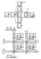
- FIG. 1 illustrates an overview of the hierarchical structure of the configurable logic array embodying the inventions hereof.
- the array of the illustrated embodiment consists of 10,000 core cells CC, all of which can be used as a simple NAND gate.
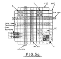
- a matrix array of 10 by 10 core cells CC with associated port cells constitutes a zone 11 (see Figure 5a) of which there are 100 in the illustrated embodiment.
- a matrix array of 5 by 5 zones constitutes a quadrant 13. In the illustrated embodiment the quadrants are disposed in a 2 by 2 matrix array.
- Inter-quadrant switches (generally designated by reference SG see Figure 8) are provided between the adjacent quadrants.
- the array is also provided with user input output cells designated by blocks 17 ( Figure 1) and the illustrated embodiment has 50 per side. Also provided are input/output multiplexers 18.
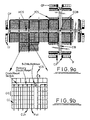
- the circuit also has a clock structure (including clock pads CP and clock bus CB) which is described further with reference to Figures 9a and 9b.
- each cell comprises a two-input-NAND gate N1, multiplexer means M1, 2, 3 and 4 on the input side and inverters I1, 12 between respective multiplexers M1, M3, M2, M4.
- Each cell also has an output multiplexer MO.
- each core cell has an extra function box (fn) that can be selected during configuration.
- fn extra function box
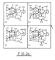
- the 4 cells making up a tile are designated by the numbers 1, 2, 3 and 4 respectively (see Figures 2a, 2b) denoting different types of core cell (ie. CC-1, CC-2, CC-3, CC-4).
- the alternative function available to the type 1 cell is a wired-OR configuration
- the additional function available to the type 2 cell is that of XOR as well having circuitry to provide half of a 2-to-1 multiplexer, or fast carry logic.
- the CIN input is driven from the type 4 cell of the tile below.
- the COUT output is input to the type 4 cell above.
- the CIN and COUT signals form the first carry logic.
- the type 3 cell in the illustrated embodiment has two alternative available functions, namely a D flip flop or a latch (each with reset and enable).
- the type 4 cell also has as its alternative function the x-OR function and additionally has the other half of the circuitry providing a 2-to-1 multiplexer or fast carry logic.
- the multiplexer and fast carry alternative functions require 2 core cells, thus the circuitry of the type 2 and type 4 cells are used together.
- the wired-OR output driver of type 1 cell is to be regarded as an alternative function although strictly speaking it is not a true alternative function in the sense of the other functions.
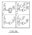
- Figure 2b shows circuitry representative of the functions available to the 4 types of core cell.
- the tiles are arranged into zones as mentioned above and connections within zones are made using local interconnect described further with reference to Figure 3, or medium range interconnect to anywhere in the zone.
- the latter comprise horizontal and vertical medium buses M which run the length and breadth of each zone (4 per row and column of cells). These are designated as M1, M2, M3, M4.
- Port cells (VPC and HPC) Figures 5, 5a, 5b, 6 and 7) at the edge of each zone make connections via the medium buses to neighbouring zones or to the global bus network.
- Horizontal and vertical x buses (referenced x) Figures 5 and 5b) also run the length and breadth of each zone (1 per row and column of cells) and in conjunction with a switch (not illustrated) in each core cell they are used for making right angled turns on these buses.
- Global buses G ( Figure 5a) run the length and breadth of each quadrant and in the illustrated embodiment there are 4 per row and column of core cells identified as G1, G2, G3 and G4 ( Figures 5a, 6 and 7). Switches SG1...SG4 ( Figure 8) between the quadrants allow global buses to run the whole length of the device if required.
- all devices will have 4 quadrants but the number of zones in each quadrant may differ from one device to another. It is however preferred to have a matrix of 10 by 10 core cells to each zone.
- the global resources available to the array comprise the global interconnect lines G1...G4 and associated switches SG1...SG4.
- the additional letters V and H are used throughout to denote vertical and horizontal connections, cells and switches etc. as the case may be.
- Global resources further comprise the above-mentioned x buses described further herein below and port cells that connect between global and zone resources. There are 10 port cells along the top of each zone (the vertical port cells VPC) and 10 along the right hand side (the horizontal port cells HPC). Connections between routing resources within zones via the medium buses M1...M4 and the global resources are only possible through the port cells. Port cells also support connections between medium buses in adjacent zones and are used for clock and tristate net distribution described further hereinafter.
- Port cells are arranged in pairs, aligned with the core cell tiling.
- Four routes are possible through each port cell - multiplexers A and C support one route each, and multiplexer B (shown as B1 and B2) supports two separate connections.
- Two of the zone medium buses (M1 and M2) are used for connections to the global and x buses through multiplexers A and C.
- M1 and M2 from the adjacent column in the tile also connect to A and C. This arrangement allows a cross over connection between pairs of port cells.
- Multiplexers A and C also provide bufferred connections from M1/M2 or M1/M2 in the column from the adjacent column in the tile to or from M3/4 in the zone above.
- the other two zone medium buses (M3 and M4) connect to multiplexers B1 and B2.
- B1 and 2 allow two independent unbufferred links to M3 or M4 in the zone above.
- M3 and M4 can be interchanged using a programmable twist.
- Alternate port cells have either a clock (CLK) or a reset (RST) multiplexer. These select the source for the dedicated clock and reset lines to the D flip flop and latch core cells, ie. the type 3 cells.
- the clock or reset multiplexer provides programmable inversion of clock and reset.
- FIG. 7a here will illustrate the connections at the top and bottom edges of the array.
- VPC vertical port cell
- input/output cells 17 by way of the input/output multiplexers 18.
- the lines emerging from the two horizontal port cells correspond to those of Figure 7 and that each port cell connects with a respective 7:1 multiplexer.
- the two x buses from each port cell have a branch into the 2:1 multiplexer which communicates with control circuitry.
- the lines passing over the zone boundary also connect with input/output cells 17 via multiplexers.
- For two adjacent cells also comprises a respective 7:1 multiplexer and a common 2:1 multiplexer.
- the lines comprise Global lines (G1...4), the x bus and medium interconnect lines M3, M4.
- the respective x buses are branched to the 2:1 multiplexer as at the top edge. Note in each case one 7:1 multiplexer feeds to an output cell 17 OUT and one is fed from an input cell 17 IN.
- the input/output connection at the edges mirror the connections between zones. This is not to be taken as limiting, merely an example and the connection to the input/output multiplexers may be for more extensive.
- the medium interconnect lines may be substituted for M3, M4 or supplement them.
- the medium interconnect lines M1, M2 terminate at the lowermost cell of each zone, ie. they do not pass over the zone boundary.
- connections to the input/output cells of the right and left edges of the array mirror the connections to the horizontal port cells (HPC) as illustrated in Figure 6 in a corresponding manner to the arrangement of Figure 7b, utilising two 7:1 multiplexers for each pair of adjacent cells and a corresponding 2:1 multiplexer for the x buses.
- HPC horizontal port cells
- Primary clocks may originate external to the device via 8 special purpose-clock pads CP or from the array by routing on general resource to the clock pads.
- the clock pads CP are situated at the corner of each quadrant (see Figure 1) and illustrated in further detail with reference to Figure 9a which is a chip level diagram.
- the clock bus CB runs vertically between the top and bottom clock pads CP and connects with a horizontal clock spine HCS (having 8 lines) running between the horizontal clock pads to opposite sides of the array.
- a central clock buffer CCB is disposed at the intersection of the vertical clock bus CB and the horizontal clock spine or bus (HCS).
- a total of 8 global signals (clocks or reset clocks) may be driven; these can be either internally or externally generated.
- Any normal user I/O input signal may also be used as a primary clock by simply routing it internally to one of the clock pads.
- the horizontal clock spine is tapped off at various points to drive multiple vertical clock spines VCS which run between adjacent zones to provide one vertical channel of 8 global clock signals per column of array zones.
- VCS vertical clock spines
- the I/O zones to the top and bottom of the array connect to the vertical clock distribution channels driven up and down through the array.
- the primary clock and reset signals are input into the vertical port cells of each zone via the zone clock and reset cells.
- An 8-2 multiplexer ( Figure 9b) distributes signals from the VCS into the vertical port cell VPC and as described with reference to Figure 7 alternate core cells CC have a clock switch or a reset switch whereby clock (CLK) or reset (RST) signals can be distributed vertically through the zone (see also Figure 9b).
- Secondary clocks can also be provided using conventional routing resource of the circuit.
- a routing comb is created by the software consisting of the horizontal spine and vertical teeth.
- the spine and teeth are routed on global interconnect and connected via x bus switches.
- the global interconnect may be extended across quadrant switches.
- the clocks are input into zones via the zones vertical port cells (which also provide programmable clock inversion), the clock can only be connected to flip flops on the same column as the secondary clock.
- Tertiary clocks may also be provided using conventional routing resource and our input into zones via the zones vertical port cells and can be routed on any level of interconnect.
- FIG. 6 illustrates detailing of the horizontal port cell HPC.
- the horizonal port cell contains no clock/reset logic. Instead, it provides support for tristate buses. Tristates are implemented using a dedicated horizontal bus within the zone (the WO bus) plus the horizonal global interconnect. The wired -OR output from the type 1 cell subsidiary function is connected to the horizontal port cell via the dedicated horizontal WO bus.
- the WO bus connects to multiplexer C in the horizontal port cells.
- the internal multiplexers for normal interconnect are the same as those for the vertical port cells.
- the functional tiling within the zones means that only half the core cell rows contain core cells with wired-OR drivers. Therefore, there are only five wired-OR buses per zone. This means that there have to be two types of port cell, one with zone wired-OR bus connecting to it (type 1), and one without (type 2).
- the zone wired-OR bus from the type 1 horizontal port cell is fed to the type 2 cell as indicated by line F.
- a WO bus can drive into horizontal global buses in every row.
- the x bus can also make a wired-OR connection onto the global buses, allowing vertical steps between wired-OR buses. This connection can be inverted as required to maintain the sense of signals.
- horizonal and vertical global buses run across each quadrant connecting to each zone via its port cells, see Figures 5, 5a, 6 and 7.
- the global buses connect to the I/O cells at the periphery of the device.
- I/O cells 17 There are 200 user configurable I/O cells 17 and these are arranged so that they pitch match 1 to every two core cells around the edges of the device.
- Global, medium and x buses (G1...G4, M1...M2 or M3...M4, X) from one core cell row or column are used as inputs and G1...G4, M1...M2 or M3...M4 and X from the adjacent row or column are used as outputs.
- An 8 bit peripheral bus runs around the whole device which is accessed by the I/O cells. Each I/O cell can read or write any of the 8 bits. Wired-OR buffers can optionally be selected when writing to the peripheral bus.
- each core cell can be connected to the outputs of nearby cells using the network of local interconnect. This provides the fastest connections between cells.
- the multiplexer A provides inputs to the core cell C from the outputs of cells U, LL, F, FB and FF
- the multiplexer B provides inputs to the core cell C from the outputs of cells UU, L, F, FB and FBB.
- each cell connects with its eight nearest perpendicular neighbours.
- Each cell C will have a set of local connection possibilities. Ie. each cell connects with only some of the other cells in a manner described in US 4 935 734 A.
- FIG 4 this illustrates how medium interconnect is used for connections within a zone that are not possible with local interconnect.
- Medium buses are also used for interzone connections since they connect to the port cells.
- M3 and M4 "the internal" medium buses, are used for connections through the port cells to all four adjacent zones as will be apparent from reference to Figure 6 and 7.
- Each of the two input multiplexers in a core cell provides connections from two medium buses.
- the core cell output multiplexers can connect to four medium buses. Therefore each individual core cell can only access half the 8 medium buses that cross each cell. To compensate for this there is a tiling of bus connections, using two different sets of connections, repeated in a 2 by 2 tile similar to the core cell functional tiling.
- each core cell in the tile connects to its horizontal and vertical medium buses as set out in table 1 below.
- Figure 10 illustrates diagrammatically for illustrative purposes the hierarchy of interconnect and shows three interconnect structures, namely firstly, the local interconnect structures which only have the scope of a few cells, and cannot connect to port cells, secondly the medium interconnect structures (M) which only have the scope of a single zone but can directly connect with port cells and core cell, and thirdly the global interconnect (G) which can span the whole array but cannot connect to core cells (CC). It will be apparent that these three levels of interconnect will be brought about by the existence of the porting arrangement that separates the array into zones. The global level of interconnect is separated from the medium and local levels of interconnect by the porting arrangement.
- M medium interconnect structures
- G global interconnect
Landscapes
- Physics & Mathematics (AREA)
- Mathematical Physics (AREA)
- Engineering & Computer Science (AREA)
- Computer Hardware Design (AREA)
- Computing Systems (AREA)
- General Engineering & Computer Science (AREA)
- Computer Networks & Wireless Communication (AREA)
- Logic Circuits (AREA)
- Design And Manufacture Of Integrated Circuits (AREA)
- Semiconductor Memories (AREA)
Claims (36)
- Konfigurierbarer Halbleiter-IC (integrated circuit: integrierter Schaltkreis), umfassend eine Fläche beziehungsweise einen Bereich mit einer Mehrzahl logischer Schaltungen an diskreten Orten beziehungsweise Sites beziehungsweise Zellen, wobei alle logischen Schaltungen eine begrenzte Fähigkeit zu einfachen Logikfunktionen gemeinsam haben und selbst nur zur Umsetzung einer einfachen Logikfunktion in der Lage sind und wobei die Zellen ein beschränktes System zur Signalleitung beziehungsweise - übersetzung zwischen Ein- und Ausgängen der logischen Schaltungen aufweisen, das lokale, direkte Verbindungswege bietet, von denen jeder bzgl. seines Leitungszustandes wählbar ist, wobei sich diese Wege für jede logische Schaltung von ihrem Ausgang zu Eingängen eines ersten Satzes aus einigen der anderen logischen Schaltungen sowie von ihren Eingängen zu Ausgängen eines zweiten Satzes aus einigen der anderen logischen Schaltungen erstrecken, wobei jeder erste Satz logischer Schaltungen von jedem anderen ersten Satz logischer Schaltungen verschieden ist und jeder zweite Satz von logischen Schaltungen von jedem anderen zweiten Satz von logischen Schaltungen verschieden ist und wobei der integrierte Schaltkreis weiter an jeder diskreten Site oder Zelle zusätzliche optional auswählbare Schaltungskonfigurationen umfasst, die mit Steuerungsmitteln selektiv steuerbar sind, um jede Zelle in die Lage zu versetzen, in einer ausgewählten von zwei oder mehr Weisen zu arbeiten, dadurch gekennzeichnet, dass eine Mehrzahl unterschiedlicher optionaler Schaltungskonfigurationen vorgesehen ist und wobei die Zellen in Gruppen angeordnet sind, die im Folgenden als Kacheln (T: tile) angesprochen werden und kleiner als das gesamte Array sind, wobei jede Kachel wenigstens eine von jeder der unterschiedlichen Schaltungskonfigurationen aufweist und wobei die Kacheln aus Zellen derart angeordnet sind, dass sie das Array einheitlich beziehungsweise gleichmäßig abdecken.
- Halbleiter-IC nach Anspruch 1, bei dem die ausgewählte von zwei oder mehr Weisen entweder die allen Zellen gemeinsame, einfache Logikfunktion oder eine ausgewählte Zusatzfunktion sein kann, die die optional auswählbare Schaltungskonfiguration ausführen kann.
- Halbleiter-IC nach den Ansprüchen 1 bis 2, bei dem die gemeinsame, einfache Logikfunktion ein NAND-Gatter ist.
- Halbleiter-IC nach den Ansprüchen 1 bis 3, bei dem die optional auswählbaren Schaltungskonfigurationen optional folgenden Funktionen ausführen können: wired-OR Ausgangspuffer, XOR, D-Typ Flip-Flop mit "reset" und "enable" und eine Latch-Funktion mit "reset" und "enable".
- Halbleiter-IC nach einem der Ansprüchen 1 bis 4, bei dem einige Zellen zusätzliche Schaltungskonfigurationen aufweisen können, um durch die Kachelanordnung die Ausbildung von Funktionen höherer Ebene zu erleichtern.
- Halbleiter-IC nach Anspruch 4, bei dem zwei XOR-Funktionen für eine Kachel vorgesehen sind.
- Halbleiter-IC nach Anspruch 4 oder 5, bei dem eine Zelle optional zwei Funktionen bietet, vorzugsweise das D-Flip-Flop und den Latch.
- Halbleiter-IC nach einem der Ansprüche 1 bis 7, bei dem die Kachel vier Zellen umfasst.
- Halbleiter-IC nach Anspruch 8, bei dem die vier Zellen in einer Matrix von 2 x 2 Zellen angeordnet sind.
- Halbleiter-IC nach Anspruch 1, bei dem die Zusatzfunktions-Anordnung innerhalb der Zellen der Kachel im Wesentlichen unterschiedlich ist.
- Halbleiter-IC nach den Ansprüchen 3 bis 8, bei dem eine Fläche beziehungsweise ein Bereich mit einer Mehrzahl logischer Schaltungen an diskreten Orten beziehungsweise Sites beziehungsweise Zellen (CC: core cells) ausgebildet ist, die das Matrix-Array von Zellen definieren, dadurch gekennzeichnet, dass das Matrix-Array von Zellen in wenigstens zwei Zonen (11) unterteilt ist, von denen jede ein Matrix-Array aus besagten Zellen und weiter eine Port-Anordnung (VPC, HPC) für jede Zone umfasst, wobei der integrierte Schaltkreis eine hierarchische Routingressourcenstruktur aufweist, welche umfasst:(i) globale Verbindungswege (G), die sich durchgehend über mehr als eine Zone erstrecken und wählbare Verbindungen mit den Port-Anordnungen wenigstens einiger der Zonen aufweisen,(ii) Mittelstrecken-Verbindungswege (M), die sich von der Port-Anordnung aus erstrecken und mit wenigstens einigen der Zellen in einer Zone auswählbar verbindbar sind und(iii) lokale Direktverbindungswege, die für jede Zelle ein beschränktes Signalleitungssystem zwischen Ein- und Ausgängen der Zellen umfassen und von denen jeder in Bezug auf seinen Leitungszustand wählbar ist, wobei sich diese Wege für jede der logischen Schaltungen von ihrem Ausgang zu Eingängen eines ersten Satzes aus einigen der anderen logischen Schaltungen sowie von ihren Eingängen zu Ausgängen eines zweiten Satzes aus einigen der anderen logischen Schaltungen erstrecken, wobei jeder erste Satz logischer Schaltungen von jedem anderen ersten Satz logischer Schaltungen verschieden ist und jeder zweite Satz logischer Schaltungen von jedem anderen zweiten Satz logischer Schaltungen verschieden ist.
- Halbleiter-IC nach einem der Ansprüche 2 bis 9, soweit abhängig von Anspruch 1, bei dem die Mehrzahl logischer Schaltungen an diskreten Orten beziehungsweise Sites beziehungsweise Zellen (CC) ein Matrix-Array von Zellen definieren, dadurch gekennzeichnet, dass das Matrix-Array von Zellen wenigstens in Zonen (11) unterteilt ist, von denen jede ein Matrix-Array aus besagten Zellen und weiter eine Port-Anordnung (VPC, HPC) für jede Zone enthält, wobei der hergestellte integrierte Schaltkreis eine hierarchische Routingressourcenstruktur aufweist, umfassend:(i) globale Verbindungswege (G), die sich durchgehend über mehr als eine Zone erstrecken und auswählbare Verbindungen mit der Port-Anordnung wenigstens einiger der Zonen aufweisen,(ii) Mittelstrecken-Verbindungswege (M), die sich von der Port-Anordnung aus erstrecken und mit wenigstens einigen der Zellen in einer Zone auswählbar verbindbar sind, und(iii) die lokalen Direktverbindungswege.
- Halbleiter-IC nach Anspruch 11 oder 12, bei dem die Zonen in einem Matrix-Array von Zonen (11) angeordnet sind.
- Halbleiter-IC nach Anspruch 11, 12 oder 13, bei dem die Mehrzahl von Zonen einen Quadranten (13) definieren und der integrierte Schaltkreis eine Mehrzahl von Quadranten umfasst.
- Halbleiter-IC nach Anspruch 14, bei dem die Quadranten in einem Matrix-Array angeordnet sind.
- Halbleiter-IC nach den Ansprüchen 11 bis 15, bei dem 10 x 10 Zellen für eine Zone, 5 x 5 Zonen für einen Quadranten und 2 x 2 Quadranten vorgesehen sind.
- Halbleiter-IC nach einem der Ansprüche 11 bis 16, bei dem sich die globalen Verbindungswege (G1...4H, G1...4V) horizontal und vertikal über eine Mehrzahl von Zonen erstrecken.
- Halbleiter-IC nach einem der Ansprüche 11 bis 17, bei dem für jede Zeile und Spalte von Zellen in einer Zone eine Mehrzahl globaler Verbindungswege vorgesehen ist.
- Halbleiter-IC nach Anspruch 18, bei dem für jede Zeile und Spalte von Zellen vier globale Verbindungswege (G1...4) vorgesehen sind.
- Halbleiter-IC nach einem der Ansprüche 11 bis 19, bei dem für jede Zeile und Spalte von Zellen einer Zone eine Mehrzahl von Mittelstrecken-Verbindungswegen (M) vorgesehen ist.
- Halbleiter-IC nach Anspruch 20, bei dem für jede Zeile und Spalte vier Mittelstrecken-Verbindungswege vorgesehen sind.
- Halbleiter-IC nach einem der Ansprüche 11 bis 21, bei dem jeder Mittelstrecken-Verbindungsweg mit einem Ausgang und/oder einem Eingang einer oder mehrerer Zellen wählbar verbindbar ist.
- Halbleiter-IC nach einem der Ansprüche 11 bis 22 umfassend weitere globale Routingressourcen, umfassend horizontale und vertikale Busse (X), die sich horizontal beziehungsweise vertikal über eine Zone erstrecken und die mit den Port-Zellen und untereinander verbindbar sind.
- Halbleiter-IC nach Anspruch 23, bei dem die weiteren horizontalen und vertikalen Busse nicht mit den Zellen verbindbar sind.
- Halbleiter-IC nach Anspruch 23 oder 24, bei dem für jede Zeile und Spalte von Zellen einer dieser weiteren globalen Verbindungsbusse vorgesehen ist.
- Halbleiter-IC nach Anspruch 25, bei dem für jede Zelle eine Verbindung zwischen den horizontalen und vertikalen Bussen vorgesehen ist.
- Halbleiter-IC nach einem der Ansprüche 11 bis 26, umfassend horizontale und vertikale Port-Zellen (HPC, VPC), deren Port-Anordnung es zu routenden Ressourcen gestattet, von den globalen Leitungen zu den Mittelstrecken-Verbindungsleitungen und dadurch in die Zellen geroutet zu werden.
- Halbleiter-IC nach einem der Ansprüche 11 bis 27, bei dem die allgemeine Verbindungsstruktur mittels der Port-Zellen mit einer speziellen Verbindungsstruktur, wie z.B. Taktgeber- oder Tristate-Mitteln verbindbar ist.
- Halbleiter-Schaltkreis nach einem der Ansprüche 11 bis 28, weiter umfassend Takt-Verteilungskanäle, vorzugsweise umfassend einen vertikalen Takt-Bus, der sich zwischen Takt-Pads (CP: clock pads) zur Ober- und Unterseite des Arrays erstreckt, und eine horizontale Takt-Verteilungsachse (HCS: horizontal clock distribution spine), die sich zwischen Takt-Pads zu gegenüberliegenden Seiten des Arrays erstreckt und den vertikalen Takt-Bus schneidet.
- Halbleiter-IC nach Anspruch 29, bei dem für jede Zone eine vertikale Takt-Verteilungsachse (VCS: vertical clock distribution spine) vorgesehen ist, durch die Takt- und Reset-Signale zu der vertikalen Port-Zelle dieser Zone verteilt werden.
- Halbleiter-IC nach Anspruch 29 oder 30, bei dem einander abwechselnde Core-Zellen Takt- und Reset-Signalleitungen aufweisen.
- Halbleiter-IC nach einem der Ansprüche 11 bis 31, bei dem alle Zellen eine gemeinsame Logikfunktion und wenigstens eine Zusatzfunktion aufweisen, wobei es wenigstens zwei verschiedene Zusatzfunktionen gibt, wobei die Core-Zellen in Kacheln (T) gruppiert sind, die ein Matrix-Array aus den Core-Zellen (CC) umfassen, und wobei jede Kachel wenigstens eine von jeder der verschiedenen Zusatzfunktionen aufweist.
- Halbleiter-IC nach Anspruch 32, bei dem die unterschiedlichen Zusatzfunktionen umfassen: wired-OR-, XOR-, D-Typ Flip-Flop- und Latch-Funktionen.
- Halbleiter-IC nach Anspruch 32 oder 33, soweit abhängig von Anspruch 22, umfassend bestimmte Verbindungsleitungen mit der horizontalen Port-Zelle, die über jede Zone verlaufen und eine Direktverbindung zu den wired-OR-Core-Zellen bilden.
- Halbleiter-IC nach Anspruch 34, bei dem eine Verbindung der wired-OR-Busse mit einer gewissen Anzahl globaler Busse hergestellt werden kann, beispielsweise über die horizontalen Port-Zellen.
- Halbleiter-IC nach Anspruch 28, soweit abhängig von Anspruch 23, bei dem wired-OR-Verbindungen zwischen den weiteren globalen, horizontalen Bussen und z.B. drei horizontalen, globalen Bussen vorgesehen sind.
Applications Claiming Priority (3)
| Application Number | Priority Date | Filing Date | Title |
|---|---|---|---|
| GB9312674 | 1993-06-18 | ||
| GB939312674A GB9312674D0 (en) | 1993-06-18 | 1993-06-18 | Configurabel logic array |
| EP94303952A EP0630115B1 (de) | 1993-06-18 | 1994-06-01 | Konfigurierbares logisches Feld |
Related Parent Applications (2)
| Application Number | Title | Priority Date | Filing Date |
|---|---|---|---|
| EP94303952A Division EP0630115B1 (de) | 1993-06-18 | 1994-06-01 | Konfigurierbares logisches Feld |
| EP94303952.9 Division | 1994-06-01 |
Publications (3)
| Publication Number | Publication Date |
|---|---|
| EP0776093A2 EP0776093A2 (de) | 1997-05-28 |
| EP0776093A3 EP0776093A3 (de) | 1997-06-18 |
| EP0776093B1 true EP0776093B1 (de) | 2002-12-04 |
Family
ID=10737437
Family Applications (2)
| Application Number | Title | Priority Date | Filing Date |
|---|---|---|---|
| EP97101407A Expired - Lifetime EP0776093B1 (de) | 1993-06-18 | 1994-06-01 | Konfigurierbares logisches Feld |
| EP94303952A Expired - Lifetime EP0630115B1 (de) | 1993-06-18 | 1994-06-01 | Konfigurierbares logisches Feld |
Family Applications After (1)
| Application Number | Title | Priority Date | Filing Date |
|---|---|---|---|
| EP94303952A Expired - Lifetime EP0630115B1 (de) | 1993-06-18 | 1994-06-01 | Konfigurierbares logisches Feld |
Country Status (12)
| Country | Link |
|---|---|
| US (1) | US5903165A (de) |
| EP (2) | EP0776093B1 (de) |
| JP (1) | JP3547168B2 (de) |
| KR (1) | KR100340310B1 (de) |
| AT (2) | ATE229245T1 (de) |
| AU (1) | AU685100B2 (de) |
| CA (1) | CA2125307A1 (de) |
| DE (2) | DE69426546T2 (de) |
| GB (2) | GB9312674D0 (de) |
| RU (1) | RU94021641A (de) |
| SG (2) | SG88743A1 (de) |
| TW (1) | TW242192B (de) |
Families Citing this family (68)
| Publication number | Priority date | Publication date | Assignee | Title |
|---|---|---|---|---|
| US5457410A (en) | 1993-08-03 | 1995-10-10 | Btr, Inc. | Architecture and interconnect scheme for programmable logic circuits |
| US6462578B2 (en) | 1993-08-03 | 2002-10-08 | Btr, Inc. | Architecture and interconnect scheme for programmable logic circuits |
| US6051991A (en) * | 1993-08-03 | 2000-04-18 | Btr, Inc. | Architecture and interconnect scheme for programmable logic circuits |
| GB9403030D0 (en) * | 1994-02-17 | 1994-04-06 | Austin Kenneth | Re-configurable application specific device |
| CN1101082C (zh) * | 1994-04-14 | 2003-02-05 | Btr公司 | 用于可编程逻辑电路的结构和互连方案 |
| CN1117432C (zh) | 1995-05-03 | 2003-08-06 | Btr公司 | 可缩放的多层互联结构 |
| US5850564A (en) * | 1995-05-03 | 1998-12-15 | Btr, Inc, | Scalable multiple level tab oriented interconnect architecture |
| US5900743A (en) | 1995-05-17 | 1999-05-04 | Altera Corporation | Programmable logic array devices with interconnect lines of various lengths |
| US5909126A (en) * | 1995-05-17 | 1999-06-01 | Altera Corporation | Programmable logic array integrated circuit devices with interleaved logic array blocks |
| US5543732A (en) * | 1995-05-17 | 1996-08-06 | Altera Corporation | Programmable logic array devices with interconnect lines of various lengths |
| US5652529A (en) * | 1995-06-02 | 1997-07-29 | International Business Machines Corporation | Programmable array clock/reset resource |
| US5631578A (en) * | 1995-06-02 | 1997-05-20 | International Business Machines Corporation | Programmable array interconnect network |
| US5671432A (en) * | 1995-06-02 | 1997-09-23 | International Business Machines Corporation | Programmable array I/O-routing resource |
| GB2305759A (en) * | 1995-09-30 | 1997-04-16 | Pilkington Micro Electronics | Semi-conductor integrated circuit |
| US5835998A (en) * | 1996-04-04 | 1998-11-10 | Altera Corporation | Logic cell for programmable logic devices |
| US5872463A (en) * | 1996-04-04 | 1999-02-16 | Altera Corporation | Routing in programmable logic devices using shared distributed programmable logic connectors |
| US6094066A (en) * | 1996-08-03 | 2000-07-25 | Mission Research Corporation | Tiered routing architecture for field programmable gate arrays |
| US6034547A (en) | 1996-09-04 | 2000-03-07 | Advantage Logic, Inc. | Method and apparatus for universal program controlled bus |
| US6624658B2 (en) | 1999-02-04 | 2003-09-23 | Advantage Logic, Inc. | Method and apparatus for universal program controlled bus architecture |
| US5880597A (en) * | 1996-09-18 | 1999-03-09 | Altera Corporation | Interleaved interconnect for programmable logic array devices |
| US6300794B1 (en) | 1996-10-10 | 2001-10-09 | Altera Corporation | Programmable logic device with hierarchical interconnection resources |
| US5977793A (en) * | 1996-10-10 | 1999-11-02 | Altera Corporation | Programmable logic device with hierarchical interconnection resources |
| US5999016A (en) * | 1996-10-10 | 1999-12-07 | Altera Corporation | Architectures for programmable logic devices |
| US6427156B1 (en) * | 1997-01-21 | 2002-07-30 | Xilinx, Inc. | Configurable logic block with AND gate for efficient multiplication in FPGAS |
| US5999015A (en) * | 1997-02-20 | 1999-12-07 | Altera Corporation | Logic region resources for programmable logic devices |
| US5982195A (en) * | 1997-02-20 | 1999-11-09 | Altera Corporation | Programmable logic device architectures |
| US7148722B1 (en) | 1997-02-20 | 2006-12-12 | Altera Corporation | PCI-compatible programmable logic devices |
| US6127844A (en) | 1997-02-20 | 2000-10-03 | Altera Corporation | PCI-compatible programmable logic devices |
| US5942913A (en) * | 1997-03-20 | 1999-08-24 | Xilinx, Inc. | FPGA repeatable interconnect structure with bidirectional and unidirectional interconnect lines |
| US6201410B1 (en) | 1997-02-26 | 2001-03-13 | Xilinx, Inc. | Wide logic gate implemented in an FPGA configurable logic element |
| US5914616A (en) * | 1997-02-26 | 1999-06-22 | Xilinx, Inc. | FPGA repeatable interconnect structure with hierarchical interconnect lines |
| US5889411A (en) * | 1997-02-26 | 1999-03-30 | Xilinx, Inc. | FPGA having logic element carry chains capable of generating wide XOR functions |
| US5963050A (en) | 1997-02-26 | 1999-10-05 | Xilinx, Inc. | Configurable logic element with fast feedback paths |
| US6204689B1 (en) | 1997-02-26 | 2001-03-20 | Xilinx, Inc. | Input/output interconnect circuit for FPGAs |
| US5920202A (en) * | 1997-02-26 | 1999-07-06 | Xilinx, Inc. | Configurable logic element with ability to evaluate five and six input functions |
| US6184710B1 (en) | 1997-03-20 | 2001-02-06 | Altera Corporation | Programmable logic array devices with enhanced interconnectivity between adjacent logic regions |
| US6084427A (en) * | 1998-05-19 | 2000-07-04 | Altera Corporation | Programmable logic devices with enhanced multiplexing capabilities |
| US6107824A (en) * | 1997-10-16 | 2000-08-22 | Altera Corporation | Circuitry and methods for internal interconnection of programmable logic devices |
| US6107825A (en) * | 1997-10-16 | 2000-08-22 | Altera Corporation | Input/output circuitry for programmable logic devices |
| US6121790A (en) | 1997-10-16 | 2000-09-19 | Altera Corporation | Programmable logic device with enhanced multiplexing capabilities in interconnect resources |
| US6218859B1 (en) * | 1998-05-26 | 2001-04-17 | Altera Corporation | Programmable logic device having quadrant layout |
| CN1180667C (zh) * | 1998-07-20 | 2004-12-15 | 三星电子株式会社 | 无线电-电子部件 |
| US6353920B1 (en) * | 1998-11-17 | 2002-03-05 | Xilinx, Inc. | Method for implementing wide gates and tristate buffers using FPGA carry logic |
| US6215326B1 (en) | 1998-11-18 | 2001-04-10 | Altera Corporation | Programmable logic device architecture with super-regions having logic regions and a memory region |
| US6507216B1 (en) | 1998-11-18 | 2003-01-14 | Altera Corporation | Efficient arrangement of interconnection resources on programmable logic devices |
| US6191612B1 (en) * | 1998-11-19 | 2001-02-20 | Vantis Corporation | Enhanced I/O control flexibility for generating control signals |
| JP3616518B2 (ja) | 1999-02-10 | 2005-02-02 | 日本電気株式会社 | プログラマブルデバイス |
| US6407576B1 (en) | 1999-03-04 | 2002-06-18 | Altera Corporation | Interconnection and input/output resources for programmable logic integrated circuit devices |
| WO2000069072A1 (en) * | 1999-05-07 | 2000-11-16 | Morphics Technology Inc. | Apparatus and methods for dynamically defining variably sized autonomous sub-arrays within a programmable gate array |
| US6320412B1 (en) | 1999-12-20 | 2001-11-20 | Btr, Inc. C/O Corporate Trust Co. | Architecture and interconnect for programmable logic circuits |
| US6657457B1 (en) * | 2000-03-15 | 2003-12-02 | Intel Corporation | Data transfer on reconfigurable chip |
| JP2001319976A (ja) * | 2000-05-11 | 2001-11-16 | Nec Corp | 半導体装置 |
| US6724810B1 (en) | 2000-11-17 | 2004-04-20 | Xilinx, Inc. | Method and apparatus for de-spreading spread spectrum signals |
| US6653862B2 (en) | 2001-05-06 | 2003-11-25 | Altera Corporation | Use of dangling partial lines for interfacing in a PLD |
| US6605962B2 (en) | 2001-05-06 | 2003-08-12 | Altera Corporation | PLD architecture for flexible placement of IP function blocks |
| US6876227B2 (en) * | 2002-03-29 | 2005-04-05 | Parama Networks, Inc. | Simplifying the layout of printed circuit boards |
| JP2003297932A (ja) * | 2002-03-29 | 2003-10-17 | Toshiba Corp | 半導体装置 |
| JP2003338750A (ja) * | 2002-05-20 | 2003-11-28 | Nec Electronics Corp | 汎用ロジックセル、これを用いた汎用ロジックセルアレイ、及びこの汎用ロジックセルアレイを用いたasic |
| US6975139B2 (en) | 2004-03-30 | 2005-12-13 | Advantage Logic, Inc. | Scalable non-blocking switching network for programmable logic |
| WO2011061099A1 (en) * | 2004-04-02 | 2011-05-26 | Panasonic Corporation | Reset/load and signal distribution network |
| US7460529B2 (en) | 2004-07-29 | 2008-12-02 | Advantage Logic, Inc. | Interconnection fabric using switching networks in hierarchy |
| US7423453B1 (en) | 2006-01-20 | 2008-09-09 | Advantage Logic, Inc. | Efficient integrated circuit layout scheme to implement a scalable switching network used in interconnection fabric |
| US7737751B1 (en) * | 2006-08-25 | 2010-06-15 | Altera Corporation | Periphery clock distribution network for a programmable logic device |
| JP2008159608A (ja) * | 2006-12-20 | 2008-07-10 | Fujitsu Ltd | 半導体装置、半導体装置の製造方法および半導体装置の設計装置 |
| FR2933826B1 (fr) * | 2008-07-09 | 2011-11-18 | Univ Paris Curie | Reseau logique programmable, commutateur d'interconnexion et unite logique pour un tel reseau |
| US7999570B2 (en) | 2009-06-24 | 2011-08-16 | Advantage Logic, Inc. | Enhanced permutable switching network with multicasting signals for interconnection fabric |
| US11216022B1 (en) * | 2020-09-16 | 2022-01-04 | Gowin Semiconductor Corporation | Methods and apparatus for providing a clock fabric for an FPGA organized in multiple clock regions |
| US11614770B2 (en) | 2020-09-16 | 2023-03-28 | Gowin Semiconductor Corporation | Methods and apparatus for organizing a programmable semiconductor device into multiple clock regions |
Family Cites Families (18)
| Publication number | Priority date | Publication date | Assignee | Title |
|---|---|---|---|---|
| US4642487A (en) * | 1984-09-26 | 1987-02-10 | Xilinx, Inc. | Special interconnect for configurable logic array |
| AU593281B2 (en) | 1985-09-11 | 1990-02-08 | Motorola, Inc. | Semi-conductor integrated circuit/systems |
| US4864381A (en) * | 1986-06-23 | 1989-09-05 | Harris Corporation | Hierarchical variable die size gate array architecture |
| US4918440A (en) * | 1986-11-07 | 1990-04-17 | Furtek Frederick C | Programmable logic cell and array |
| US4969121A (en) * | 1987-03-02 | 1990-11-06 | Altera Corporation | Programmable integrated circuit logic array device having improved microprocessor connectability |
| US5109353A (en) * | 1988-12-02 | 1992-04-28 | Quickturn Systems, Incorporated | Apparatus for emulation of electronic hardware system |
| GB8828828D0 (en) | 1988-12-09 | 1989-01-18 | Pilkington Micro Electronics | Semiconductor integrated circuit |
| GB8906145D0 (en) * | 1989-03-17 | 1989-05-04 | Algotronix Ltd | Configurable cellular array |
| US5255203A (en) * | 1989-08-15 | 1993-10-19 | Advanced Micro Devices, Inc. | Interconnect structure for programmable logic device |
| JP2756325B2 (ja) * | 1989-12-07 | 1998-05-25 | 株式会社日立製作所 | クロック供給回路 |
| US5218240A (en) * | 1990-11-02 | 1993-06-08 | Concurrent Logic, Inc. | Programmable logic cell and array with bus repeaters |
| US5144166A (en) * | 1990-11-02 | 1992-09-01 | Concurrent Logic, Inc. | Programmable logic cell and array |
| JP3179800B2 (ja) * | 1991-07-22 | 2001-06-25 | 株式会社日立製作所 | 半導体集積回路装置 |
| US5208491A (en) * | 1992-01-07 | 1993-05-04 | Washington Research Foundation | Field programmable gate array |
| GB9223226D0 (en) * | 1992-11-05 | 1992-12-16 | Algotronix Ltd | Improved configurable cellular array (cal ii) |
| GB2280293B (en) * | 1993-07-19 | 1997-12-10 | Hewlett Packard Co | Architecture for programmable logic |
| US5457410A (en) * | 1993-08-03 | 1995-10-10 | Btr, Inc. | Architecture and interconnect scheme for programmable logic circuits |
| US5455525A (en) * | 1993-12-06 | 1995-10-03 | Intelligent Logic Systems, Inc. | Hierarchically-structured programmable logic array and system for interconnecting logic elements in the logic array |
-
1993
- 1993-06-18 GB GB939312674A patent/GB9312674D0/en active Pending
-
1994
- 1994-06-01 AT AT97101407T patent/ATE229245T1/de not_active IP Right Cessation
- 1994-06-01 SG SG9804165A patent/SG88743A1/en unknown
- 1994-06-01 SG SG1996001812A patent/SG64300A1/en unknown
- 1994-06-01 DE DE69426546T patent/DE69426546T2/de not_active Expired - Fee Related
- 1994-06-01 EP EP97101407A patent/EP0776093B1/de not_active Expired - Lifetime
- 1994-06-01 AT AT94303952T patent/ATE198685T1/de active
- 1994-06-01 DE DE69431848T patent/DE69431848T2/de not_active Expired - Fee Related
- 1994-06-01 EP EP94303952A patent/EP0630115B1/de not_active Expired - Lifetime
- 1994-06-01 GB GB9410980A patent/GB2279168B/en not_active Expired - Fee Related
- 1994-06-02 US US08/253,041 patent/US5903165A/en not_active Expired - Fee Related
- 1994-06-07 CA CA002125307A patent/CA2125307A1/en not_active Abandoned
- 1994-06-09 AU AU64654/94A patent/AU685100B2/en not_active Ceased
- 1994-06-15 TW TW083105389A patent/TW242192B/zh not_active IP Right Cessation
- 1994-06-17 KR KR1019940013723A patent/KR100340310B1/ko not_active Expired - Fee Related
- 1994-06-17 RU RU94021641/25A patent/RU94021641A/ru unknown
- 1994-06-20 JP JP13758794A patent/JP3547168B2/ja not_active Expired - Fee Related
Also Published As
| Publication number | Publication date |
|---|---|
| EP0630115A2 (de) | 1994-12-21 |
| JP3547168B2 (ja) | 2004-07-28 |
| ATE198685T1 (de) | 2001-01-15 |
| JPH0758631A (ja) | 1995-03-03 |
| ATE229245T1 (de) | 2002-12-15 |
| US5903165A (en) | 1999-05-11 |
| CA2125307A1 (en) | 1994-12-19 |
| DE69426546T2 (de) | 2001-07-12 |
| AU685100B2 (en) | 1998-01-15 |
| TW242192B (de) | 1995-03-01 |
| DE69426546D1 (de) | 2001-02-15 |
| AU6465494A (en) | 1994-12-22 |
| RU94021641A (ru) | 1996-06-27 |
| SG64300A1 (en) | 1999-04-27 |
| GB9410980D0 (en) | 1994-07-20 |
| EP0630115A3 (de) | 1995-03-22 |
| GB2279168B (en) | 1998-01-21 |
| EP0630115B1 (de) | 2001-01-10 |
| EP0776093A2 (de) | 1997-05-28 |
| DE69431848D1 (de) | 2003-01-16 |
| GB9312674D0 (en) | 1993-08-04 |
| KR100340310B1 (ko) | 2002-11-23 |
| KR950001990A (ko) | 1995-01-04 |
| GB2279168A (en) | 1994-12-21 |
| DE69431848T2 (de) | 2003-05-28 |
| SG88743A1 (en) | 2002-05-21 |
| EP0776093A3 (de) | 1997-06-18 |
Similar Documents
| Publication | Publication Date | Title |
|---|---|---|
| EP0776093B1 (de) | Konfigurierbares logisches Feld | |
| US7579868B2 (en) | Architecture for routing resources in a field programmable gate array | |
| US7557611B2 (en) | Block level routing architecture in a field programmable gate array | |
| EP1158402B1 (de) | FPGA mit Setz-/Rücksetzleitungen | |
| EP0819340B1 (de) | Logische zelle und verbindungsarchitektur in einem benutzerprogrammierbaren logischen feld | |
| US6335634B1 (en) | Circuitry and methods for internal interconnection of programmable logic devices | |
| US6414514B1 (en) | Logic device architecture and method of operation | |
| US6680624B2 (en) | Block symmetrization in a field programmable gate array | |
| US6838903B1 (en) | Block connector splitting in logic block of a field programmable gate array | |
| GB2305759A (en) | Semi-conductor integrated circuit | |
| AU723157B2 (en) | Configurable logic array | |
| US20080258763A1 (en) | Block symmetrization in a field programmable gate array | |
| GB2312308A (en) | Configurable logic array | |
| AU5500300A (en) | A semi-conductor integrated circuit |
Legal Events
| Date | Code | Title | Description |
|---|---|---|---|
| PUAI | Public reference made under article 153(3) epc to a published international application that has entered the european phase |
Free format text: ORIGINAL CODE: 0009012 |
|
| PUAL | Search report despatched |
Free format text: ORIGINAL CODE: 0009013 |
|
| 17P | Request for examination filed |
Effective date: 19970221 |
|
| AC | Divisional application: reference to earlier application |
Ref document number: 630115 Country of ref document: EP |
|
| AK | Designated contracting states |
Kind code of ref document: A2 Designated state(s): AT BE CH DE DK ES FR GB GR IE IT LI LU MC NL PT SE |
|
| AK | Designated contracting states |
Kind code of ref document: A3 Designated state(s): AT BE CH DE DK ES FR GB GR IE IT LI LU MC NL PT SE |
|
| RAP1 | Party data changed (applicant data changed or rights of an application transferred) |
Owner name: MOTOROLA, INC. |
|
| 17Q | First examination report despatched |
Effective date: 19990810 |
|
| GRAG | Despatch of communication of intention to grant |
Free format text: ORIGINAL CODE: EPIDOS AGRA |
|
| GRAG | Despatch of communication of intention to grant |
Free format text: ORIGINAL CODE: EPIDOS AGRA |
|
| GRAH | Despatch of communication of intention to grant a patent |
Free format text: ORIGINAL CODE: EPIDOS IGRA |
|
| GRAH | Despatch of communication of intention to grant a patent |
Free format text: ORIGINAL CODE: EPIDOS IGRA |
|
| GRAA | (expected) grant |
Free format text: ORIGINAL CODE: 0009210 |
|
| AC | Divisional application: reference to earlier application |
Ref document number: 630115 Country of ref document: EP |
|
| AK | Designated contracting states |
Kind code of ref document: B1 Designated state(s): AT BE CH DE DK ES FR GB GR IE IT LI LU MC NL PT SE |
|
| PG25 | Lapsed in a contracting state [announced via postgrant information from national office to epo] |
Ref country code: NL Free format text: LAPSE BECAUSE OF FAILURE TO SUBMIT A TRANSLATION OF THE DESCRIPTION OR TO PAY THE FEE WITHIN THE PRESCRIBED TIME-LIMIT Effective date: 20021204 Ref country code: LI Free format text: LAPSE BECAUSE OF FAILURE TO SUBMIT A TRANSLATION OF THE DESCRIPTION OR TO PAY THE FEE WITHIN THE PRESCRIBED TIME-LIMIT Effective date: 20021204 Ref country code: GR Free format text: LAPSE BECAUSE OF FAILURE TO SUBMIT A TRANSLATION OF THE DESCRIPTION OR TO PAY THE FEE WITHIN THE PRESCRIBED TIME-LIMIT Effective date: 20021204 Ref country code: CH Free format text: LAPSE BECAUSE OF FAILURE TO SUBMIT A TRANSLATION OF THE DESCRIPTION OR TO PAY THE FEE WITHIN THE PRESCRIBED TIME-LIMIT Effective date: 20021204 Ref country code: BE Free format text: LAPSE BECAUSE OF FAILURE TO SUBMIT A TRANSLATION OF THE DESCRIPTION OR TO PAY THE FEE WITHIN THE PRESCRIBED TIME-LIMIT Effective date: 20021204 Ref country code: AT Free format text: LAPSE BECAUSE OF FAILURE TO SUBMIT A TRANSLATION OF THE DESCRIPTION OR TO PAY THE FEE WITHIN THE PRESCRIBED TIME-LIMIT Effective date: 20021204 |
|
| REF | Corresponds to: |
Ref document number: 229245 Country of ref document: AT Date of ref document: 20021215 Kind code of ref document: T |
|
| REG | Reference to a national code |
Ref country code: GB Ref legal event code: FG4D |
|
| REG | Reference to a national code |
Ref country code: CH Ref legal event code: EP |
|
| REG | Reference to a national code |
Ref country code: IE Ref legal event code: FG4D |
|
| REF | Corresponds to: |
Ref document number: 69431848 Country of ref document: DE Date of ref document: 20030116 |
|
| PG25 | Lapsed in a contracting state [announced via postgrant information from national office to epo] |
Ref country code: SE Free format text: LAPSE BECAUSE OF FAILURE TO SUBMIT A TRANSLATION OF THE DESCRIPTION OR TO PAY THE FEE WITHIN THE PRESCRIBED TIME-LIMIT Effective date: 20030304 Ref country code: DK Free format text: LAPSE BECAUSE OF FAILURE TO SUBMIT A TRANSLATION OF THE DESCRIPTION OR TO PAY THE FEE WITHIN THE PRESCRIBED TIME-LIMIT Effective date: 20030304 |
|
| PG25 | Lapsed in a contracting state [announced via postgrant information from national office to epo] |
Ref country code: PT Free format text: LAPSE BECAUSE OF FAILURE TO SUBMIT A TRANSLATION OF THE DESCRIPTION OR TO PAY THE FEE WITHIN THE PRESCRIBED TIME-LIMIT Effective date: 20030305 |
|
| ET | Fr: translation filed | ||
| NLV1 | Nl: lapsed or annulled due to failure to fulfill the requirements of art. 29p and 29m of the patents act | ||
| PG25 | Lapsed in a contracting state [announced via postgrant information from national office to epo] |
Ref country code: LU Free format text: LAPSE BECAUSE OF NON-PAYMENT OF DUE FEES Effective date: 20030601 Ref country code: GB Free format text: LAPSE BECAUSE OF NON-PAYMENT OF DUE FEES Effective date: 20030601 |
|
| PG25 | Lapsed in a contracting state [announced via postgrant information from national office to epo] |
Ref country code: IE Free format text: LAPSE BECAUSE OF NON-PAYMENT OF DUE FEES Effective date: 20030602 |
|
| PGFP | Annual fee paid to national office [announced via postgrant information from national office to epo] |
Ref country code: FR Payment date: 20030602 Year of fee payment: 10 |
|
| REG | Reference to a national code |
Ref country code: CH Ref legal event code: PL |
|
| PG25 | Lapsed in a contracting state [announced via postgrant information from national office to epo] |
Ref country code: ES Free format text: LAPSE BECAUSE OF FAILURE TO SUBMIT A TRANSLATION OF THE DESCRIPTION OR TO PAY THE FEE WITHIN THE PRESCRIBED TIME-LIMIT Effective date: 20030627 |
|
| PG25 | Lapsed in a contracting state [announced via postgrant information from national office to epo] |
Ref country code: MC Free format text: LAPSE BECAUSE OF NON-PAYMENT OF DUE FEES Effective date: 20030630 |
|
| PGFP | Annual fee paid to national office [announced via postgrant information from national office to epo] |
Ref country code: DE Payment date: 20030630 Year of fee payment: 10 |
|
| PLBE | No opposition filed within time limit |
Free format text: ORIGINAL CODE: 0009261 |
|
| STAA | Information on the status of an ep patent application or granted ep patent |
Free format text: STATUS: NO OPPOSITION FILED WITHIN TIME LIMIT |
|
| 26N | No opposition filed |
Effective date: 20030905 |
|
| GBPC | Gb: european patent ceased through non-payment of renewal fee |
Effective date: 20030601 |
|
| REG | Reference to a national code |
Ref country code: IE Ref legal event code: MM4A |
|
| PG25 | Lapsed in a contracting state [announced via postgrant information from national office to epo] |
Ref country code: DE Free format text: LAPSE BECAUSE OF NON-PAYMENT OF DUE FEES Effective date: 20050101 |
|
| PG25 | Lapsed in a contracting state [announced via postgrant information from national office to epo] |
Ref country code: FR Free format text: LAPSE BECAUSE OF NON-PAYMENT OF DUE FEES Effective date: 20050228 |
|
| REG | Reference to a national code |
Ref country code: FR Ref legal event code: ST |
|
| PG25 | Lapsed in a contracting state [announced via postgrant information from national office to epo] |
Ref country code: IT Free format text: LAPSE BECAUSE OF NON-PAYMENT OF DUE FEES;WARNING: LAPSES OF ITALIAN PATENTS WITH EFFECTIVE DATE BEFORE 2007 MAY HAVE OCCURRED AT ANY TIME BEFORE 2007. THE CORRECT EFFECTIVE DATE MAY BE DIFFERENT FROM THE ONE RECORDED. Effective date: 20050601 |