EP0819340B1 - Logische zelle und verbindungsarchitektur in einem benutzerprogrammierbaren logischen feld - Google Patents
Logische zelle und verbindungsarchitektur in einem benutzerprogrammierbaren logischen feld Download PDFInfo
- Publication number
- EP0819340B1 EP0819340B1 EP96908832A EP96908832A EP0819340B1 EP 0819340 B1 EP0819340 B1 EP 0819340B1 EP 96908832 A EP96908832 A EP 96908832A EP 96908832 A EP96908832 A EP 96908832A EP 0819340 B1 EP0819340 B1 EP 0819340B1
- Authority
- EP
- European Patent Office
- Prior art keywords
- interconnect lines
- logic
- integrated circuit
- logic cell
- circuit according
- Prior art date
- Legal status (The legal status is an assumption and is not a legal conclusion. Google has not performed a legal analysis and makes no representation as to the accuracy of the status listed.)
- Expired - Lifetime
Links
- 238000012546 transfer Methods 0.000 claims description 38
- 239000000872 buffer Substances 0.000 claims description 25
- 230000006386 memory function Effects 0.000 claims description 2
- 230000006870 function Effects 0.000 description 11
- 238000013461 design Methods 0.000 description 4
- 238000004364 calculation method Methods 0.000 description 3
- 238000010586 diagram Methods 0.000 description 3
- 238000000034 method Methods 0.000 description 3
- 230000002457 bidirectional effect Effects 0.000 description 2
- 238000013459 approach Methods 0.000 description 1
- 238000003491 array Methods 0.000 description 1
- 230000005540 biological transmission Effects 0.000 description 1
- 230000007812 deficiency Effects 0.000 description 1
- 230000001934 delay Effects 0.000 description 1
- 238000012905 input function Methods 0.000 description 1
- 239000007937 lozenge Substances 0.000 description 1
- 238000012986 modification Methods 0.000 description 1
- 230000004048 modification Effects 0.000 description 1
- 238000005457 optimization Methods 0.000 description 1
- 238000012856 packing Methods 0.000 description 1
- 230000002040 relaxant effect Effects 0.000 description 1
- 230000000717 retained effect Effects 0.000 description 1
- 239000007787 solid Substances 0.000 description 1
- 239000002699 waste material Substances 0.000 description 1
Images


Classifications
-
- H—ELECTRICITY
- H03—ELECTRONIC CIRCUITRY
- H03K—PULSE TECHNIQUE
- H03K19/00—Logic circuits, i.e. having at least two inputs acting on one output; Inverting circuits
- H03K19/02—Logic circuits, i.e. having at least two inputs acting on one output; Inverting circuits using specified components
- H03K19/173—Logic circuits, i.e. having at least two inputs acting on one output; Inverting circuits using specified components using elementary logic circuits as components
- H03K19/177—Logic circuits, i.e. having at least two inputs acting on one output; Inverting circuits using specified components using elementary logic circuits as components arranged in matrix form
- H03K19/17736—Structural details of routing resources
-
- H—ELECTRICITY
- H03—ELECTRONIC CIRCUITRY
- H03K—PULSE TECHNIQUE
- H03K19/00—Logic circuits, i.e. having at least two inputs acting on one output; Inverting circuits
- H03K19/02—Logic circuits, i.e. having at least two inputs acting on one output; Inverting circuits using specified components
- H03K19/173—Logic circuits, i.e. having at least two inputs acting on one output; Inverting circuits using specified components using elementary logic circuits as components
- H03K19/177—Logic circuits, i.e. having at least two inputs acting on one output; Inverting circuits using specified components using elementary logic circuits as components arranged in matrix form
- H03K19/17704—Logic circuits, i.e. having at least two inputs acting on one output; Inverting circuits using specified components using elementary logic circuits as components arranged in matrix form the logic functions being realised by the interconnection of rows and columns
Definitions
- the present invention is related to field programmable integrated circuits, and more particularly, to Field Programmable Gate Arrays (FPGAs).
- FPGAs Field Programmable Gate Arrays
- an FPGA has an array of logic elements and wiring interconnections with many thousands, or even hundreds of thousands, of programmable switches so that the FPGA can be configured by the user into an integrated circuit with defined functions.
- Each programmable switch, or interconnect can connect two circuit nodes in the integrated circuit to make (or break) a wiring interconnection, or to set the function or functions of a logic element.
- the wiring should be designed so that the likelihood of use of each wiring segment is maximized, yet the use of wiring segments for one purpose should not be a bottleneck to wiring connections for other purposes. Furthermore, the ease of use of the routing of the wiring and the operating speeds of the configured FPGA are other considerations in the design. These factors must be weighed and balanced.
- US5465055 discloses a RAM-logic tile (RTL) for use in an FPGA, where the RTLs are located at the intersection of global horizontal and vertical lines. Wiring segments run locally between RTLs and contain programmable antifuses for connecting segments within an RTL and to neighbouring RTLs.
- the RTLs are implemented with transmission gates and can be configured into a memory structure and/or logic device.
- EP0647030 discloses a base cell device for providing all two-input functions.
- the present invention is a solution to the problem of FPGA architecture design.
- the logic cell and wiring are designed so that an FPGA with a high degree of functionality, flexibility, utilization, ease of use and operating speeds is possible. Many of the issues which have plagued FPGA architecture are solved or mitigated.
- an integrated circuit according to claim 1.
- An embodiment of the present invention provides an integrated circuit having a plurality of logic cells, interconnect lines and switches for programmably connecting said logic cells and interconnect lines, characterised in that each logic cell comprises first and second transfer gates, each transfer gate having an input node, control terminals programmably connectable to a first true or inverted signal, or to a fixed logic level, and an output node connected in common to the other transfer gate, an input node of said first transfer gate being programmably connectable to a fixed logic level or an output signal from said logic cell, an input node of said second transfer gate being programmably connectable to a second true or inverted signal, or to a fixed logic level; and a logic cell gate having a plurality of input nodes comprising a first input node connected to said commonly connected output nodes of said first and second transfer gates, a second input node programmably connectable to a third true or inverted signal, or to a fixed logic level, and an output node for generating said logic cell output signal; whereby said logic cells, individually or several
- the present invention also provides an integrated circuit having a plurality of logic cells arranged in rows and columns, each logic cell having input and output terminals.
- the integrated circuit has first global interconnect lines running through the array parallel to the columns and second global interconnect lines running through each row of the logic cells perpendicular to and intersecting the first global interconnect lines.
- the second global interconnect lines in a row are programmably connectable to at least one of the input terminals of each logic cell in the row, and to at least one of the input terminals of each logic cell in a neighbouring row.
- the second global interconnect lines are alternately programmably connectable to first and second subsets of the first global interconnect lines in alternating rows of the logic cells. This permits each logic cell to be programmably connectable through the one input terminal to any of the first global interconnect lines.
- FPGAS use either memory cells or antifuses for the programmable switches. Memory cells are reprogrammable and antifuses are programmable only once.
- the present invention is designed to be implemented with a new memory-type of programmable interconnect, as disclosed in a patent application, U.S. Appln. No. 08/270,714 , entitled, "A GENERAL PURPOSE, NON-VOLATILE REPROGRAMMABLE SWITCH,” filed July 5, 1994 by Robert J. Lipp, Richard D. Freeman, Robert U. Broze, John M. Caywood, and Joseph G. Nolan, III, and assigned to the present assignee.
- NVM non-volatile reprogrammable transistor memory
- the present invention should not be considered limited to the disclosed programmable switch only. Other types of memory cells may be used for the programmable switches. Even an antifuse-based FPGA may benefit from the present invention.
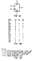
- An integrated circuit according to the present invention uses a logic cell 10, as shown in Fig. 1A .
- the logic cell 10 has a core 17, which is denoted by a dotted line.
- the core 17 has an inverter 11 which has an output node connected to the control nodes of two transfer gates 12 and 13.
- Each transfer gate is basically a PMOS and an NMOS transistor having a first common source/drain region forming the input node to the transfer gate and a second common source/drain region forming an output node of the transfer gate.
- the gate electrodes for the PMOS and NMOS transistors form the two control nodes.
- the output nodes of the transfer gates 12 and 13 are connected in common to an input node of a NAND gate 14.
- the output node of the NAND gate 14 is connected to input nodes of an inverter 15 and an optional inverter 16, which is connected in parallel to the first inverter 15.
- the inverters. 15 and 16 act as buffers for the output signal from the NAND gate 14.
- the signals on the output nodes of the inverters 15 and 16 are the same and, for the remainder of this disclosure, are considered as the output signal on the output terminal Y of the logic cell 10.
- the second inverter 16 is used for particular loads on the wiring routing from the output terminal Y. This is explained below. It should be noted that the logic cell core 17 itself contains no programmable elements; rather, the input signals to the core are controlled by programmable switches located outside the core 17 to define the function of the cell 10.
- the logic cell 10 has three input terminals, X2, X3, and X1, in descending order in the drawing.
- the input terminal X2 is connected to the input node of an inverter 43 which has its output node connected to the input node of the inverter 11 of the logic cell core by a programmable switch 25.
- the input terminal X2 is connectable to ground.
- the input terminal X2 is also connectable directly to the input node of the inverter 11.
- the input node of the inverter 11 is also connected to the PMOS gate electrode of the transfer gate 12 and the gate electrode of the NMOS transistor of the transfer gate 13.
- the input terminal X3 is connected to the input node of an inverter 42, which has its output node connectable to the input terminal of the transfer gate 13 through a programmable switch 27. Through another programmable switch 26, the input terminal X3 is also connectable directly to the input node of the transfer gate 13. The input node X3 is also connectable to ground through a programmable switch 22.
- the input terminal X1 is connected to the input node of an inverter 41 which has its output node connectable to the second input node of the NAND gate 14 through programmable switches 29 and 35.
- a programmable switch 28 which is connected in parallel to the inverter 41 and programmable switch 29, the input terminal X1 is directly connectable to the second input terminal of the NAND gate 14 through the programmable switch 35.
- the second input terminal of the NAND gate 14 is also capable of being pulled high (the positive power supply at V CC ) through a programmable switch 34. Similar to the previous input terminals X2 and X3, the input terminal X1 is also capable of being set low (the lower power supply at ground) by a programmable switch 21.
- the output terminal F from the inverter 15 is also connectable to the input node of the transfer gate 12 through a programmable switch 30.
- the input terminal of the transfer gate 12 is also capable of being set high by a programmable switch 32, or set low by a programmable switch 33.
- the input terminal of the transfer gate 12 is also connectable to the input terminal X1 through a programmable switch 31, which is connected between the programmable switches 28, 29, and 35.
- FIG. 1B A representation of the logic cell 10 as used in subsequent drawings is shown in Fig. 1B . While the other embodiments of the present invention have other number of input terminals, three input terminals are believed to be optimum based upon calculations of likely configurations.
- the cell 10 is much smaller than the cells of most of the present FPGAs. This allows a greater packing density, i.e., less area per cell, on the integrated circuit.
- the logic cell 10 has great versatility and is capable of performing many functions.
- the table in Fig. 2 illustrates the functions of the different programmable switches in the logic cell 10.
- the transfer gates 12 and 13 operate as a simple multiplexer.
- the input signal to the transfer gate 12 is described as the input signal A and the input signal to the transfer gate 13 as the input signal B.
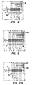
- Fig. 3A illustrates the setting of the programmable switches so that the logic cell 10 operates as a two-input AND gate.
- the programmable switches are labelled as "ON” to make the connection, while they are labelled as “OFF” to indicate that the programmable switch remains open.
- the two AND gate inputs are the signals on the X1 and X3 input terminals.
- the programmable switches for the X2 input terminal, i.e., programmable switches 23 and 25, have been set to insure that the transfer gate 13 passes the signal on the input terminal X3 to the first input node of the NAND gate 14.
- Fig. 3B illustrates another setting of the programmable switches so that the logic cell 10 operates as a D-latch with an active high clear (CLR) control signal.
- the data signal for the latch is received by the X3 input terminal and the clear signal by the X1 input terminal.
- the programmable switch 25 for the X2 input terminal is set to turn on the transfer gates 12 and 13.
- the programmable switch 30 is turned on for a feedback from the output terminal of the logic cell to complete the latch.
- the logic cell 10 can be configured to perform many other functions.
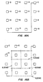
- Fig. 4A illustrates the logic cell 10 drawn as a latch.
- Fig. 4B is a list of 14 latch types which are possible with the logic cell 10, and
- Fig. 4C explains the latch-type notation used in Fig. 4B .
- Fig. 5A is a representation of the logic cell 10 configured as a D-type flip-flop.
- Fig. 5B lists 28 different possibilities of D flip-flops which are possible with the logic cell 10.
- Fig. 5C explains the notation used to denote the different types of flip-flops in Fig. 5B .
- one logic cell 10 cannot be configured to perform the desired function, more than one cell may be connected together and programmed. To make these connections, the wiring of the FPGA comes into play.
- any placement and routing architecture of wiring between logic cells in an FPGA is a balance. If a designer has infinite line and switch resources, a full crossbar network which allows the output of every cell to access the input of every cell would be the best architecture. However, simple calculations indicate that the required number of programmable switches only would occupy an inordinate amount of space, even in a array with a moderate number of logic cells. Additionally, a calculation of the average switch utilization indicates that most of the switches would not be used. On the other hand, if a routing architecture is restricted so that each cell output can only be routed to a set of inputs of a single cell, nearly any circuit which would be desired by a user could not be configured.
- the present invention minimizes the wiring resources, i.e., the wiring segments to and from the input and output terminals of the logic cells and the programmable switches for interconnecting the segments, with a maximization of the number of routable connections.
- the present invention achieves these goals by the use of overlapping windows of tiles, directional routing and programmable interconnecting tiles to make an extremely adaptable routing architecture.
- the word "tile" refers to a logic cell and its associated wiring segments and programmable switches.
- An array of tiles forms the FPGA.
- the routing architecture of the tiles is divisible into three components, local routing, long routing, and global routing.
- each 3X3 region of tiles overlaps in a manner such that the routing of the wiring segments in each tile are "self-similar" for each focal, i.e., center, tile in the 3X3 region.
- the focal tile moves with the 3X3 region, which can be anywhere in the array of tiles.
- self-similar means that the output of any focal tile can always reach the input of any other cell (including itself), in its 3X3 region of tiles by a unique, guaranteed route.
- Fig. 6 illustrates this point with an exemplary array of tiles 40.
- each tile 40 has a logic cell 10 and its associated wiring segments and programming switches.
- a solid line 41 closes a 3X3 region of tiles.
- the focal tile of this region is denoted F1.
- the output of the logic cell of F1 can reach the input of any logic cell of any tile in the region enclosed by the line 41 by a unique, guaranteed route.
- another 3X3 region is considered, here indicated by a solid line 42, with the focal tile of this region denoted F2
- the output of the logic cell in F2 can reach the input of any logic cell within the region denoted by line 42 by a unique, guaranteed route.
- the regions denoted by the lines 41 and 42 are overlapping and that every tile in the array (except for those at the periphery) is a focal tile.
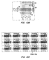
- Fig. 7A illustrates the local routing architecture of a single tile 40 according to one embodiment of the present invention.
- the input terminals X1, X2 and X3 of the logic cell 10 of the tile 40 are connected to three wiring segments, which are part of a set of nine vertical local wiring segments 43.
- the output terminal Y of the logic cell 10 is connected to one of the three horizontal local wiring segments 44.
- At the intersection of each of the vertical local wiring segments 43 and horizontal local wiring segments 44 are programmable switches, which are indicated by solid circles.
- the local wiring segments 43 and 44 of adjacent tiles connect in an overlapping manner.
- the top two segments at the right edge of the tile are connected to horizontal wiring segments 44 in horizontally adjacent tiles.
- Overlap occurs because in each tile, the bottom two segments become the top two segments as one proceeds from right to left across the tile 40.
- For the vertical local wiring segments 43 six of the nine wiring segments are connected to segments 43 in vertically adjacent tiles. At the bottom of each tile 40, the six segments are the first, second, fourth, fifth, seventh and eighth from the left. Overlap occurs because in each tile 40 these segments are respectively in the position of the second, third, fifth, sixth, eighth and ninth segments before reaching the bottom of the tile.
- Fig. 7B shows the connections of the local wiring segments 43 and 44 in a 3X3 tile region.
- the tile 40E is the focal tile of the region and its output terminal may be connected to any input terminal of a logic cell in any neighboring tile 40A-40D, 40F-40I, and itself through a single, unique programmable switch.
- Each logic cell of a focal tile has a new set of routing resources identical to its neighbors. In this embodiment, the new wiring is guaranteed to be available.
- the output of the logic cell of the focal tile can reach any or all of the 27 inputs of the neighboring logic cells, including itself.
- the ability to reach these nine cells is an advance over much of the prior art.
- the placement of functions with specific logic cells is much less constrained and the percentage of routes which may be accomplished with local routing resources is larger. It should be noted that this very high percentage of connections substantially reduces the requirements for the "long" routing resources, while allowing these wiring resources to be more flexible since they form fewer connections.
- the present local routing is very area efficient, with a high percentage of connections made with local resources and the relatively small number of switches required. The switches for local routing tend to have very high utilization.
- each tile 40 has the same arrangement of vertical local wiring segments 43 and horizontal wiring segments 44, as is shown in Fig. 7A .
- the three programmable switches at the intersections of the vertical wiring segments connected to the local cell input terminals X1, X2 and X3, and the horizontal wiring segment connected to the output terminal F have been eliminated, as shown in Fig. 8 .
- the output terminal of the logic cell of the focal tile may be connected to the input terminals of its eight adjacent neighbors, but not to the input terminals of its own logic cell. In typical applications there are very few signals which feed back to their own logic cell. If required, this feedback path may be implemented, either internally to the logic cell (note programmable switch 30 in Fig. 1A ), or by the use of a long routing resource, discussed below.
- Fig. 9 illustrates local routing with a logic cell 10A having four input terminals X1, X2, X3, X4, and a single output Y.
- the horizontal local wiring segments 48 remain at three with the output terminal Y connected to one of the segments as before.
- each local connection requires only one programmable switch. This contributes to the speed of the circuit implemented on this local "mesh" of wiring segments, since the interconnect speed is an inverse function of the number of programmable switches a signal traverses.
- the local routing as described thus far has one drawback. If a local cell output terminal does not need a connection to an input terminal of cell in one of the tiles of the local region, that path is wasted. In the worst case, an unused logic cell leaves 27 unused paths. To correct this deficiency, the local routing architecture may be modified slightly so that the output terminal of a logic cell is not required to use the local wiring segments. This permits the local wiring segments to be used for other connections; routability in the architecture is increased.
- a three-state driver 49 is added at the output terminal Y of the logic cell 10.
- the driver 49 is enabled or disabled by a programmable interconnect, not shown.
- the driver 49 is disabled, the logic cell is effectively disconnected from the horizontal wiring segments 44.
- the driver 49 is enabled, it drives the high or low logic signals from the logic cell 10 onto the connected horizontal wiring segment 44.
- each of the horizontal wiring segments 44 are connectable to the output terminal Y of the logic cell 10 by programmable switches.
- a dotted line 50 encircles the programmable switches at the intersection of the output terminal Y and the horizontal wiring segments 44.
- FIG. 10C illustrates the detailed local wiring segments in a 5X3 tile region with the focal cell of this region indicated.
- larger local tile regions may be assembled, e.g., 4X4, 5X5 and other regions. Moreover, these regions need not be square, such as 3X4, 4X5, 3X5 tile regions. Of course, each increased region increases the percentage of connections which can be made locally.
- each of the tiles has additional programmable routing resources so that connections can be made to nodes outside the local regions.
- These so-called long routing resources are completely programmable and are not shared with the local wiring segments. Approximately 66% of all routing can be made by the local routing resources; the remaining 33% can be performed by the long routing resources.
- the long wiring segments of the present invention also allows better control over the maximum path length of connected wiring, and hence the timing of signals, compared to the prior art.
- a traditional gate array with a similar capacity to the FPGA herein described requires approximately 9X12 tracks in the gate array's channels to attain 80% routability to all of the array's resources. Since 66% of the routing is being handled by the local routing resources of the FPGA of the present invention, only 3X4 tracks are required for long routing. To insure ample routability, slightly more long wiring segments are used.
- one form of tile for use in an integrated circuit uses five horizontal long wiring segments 51 and five vertical long wiring segments 52, as the long routing resources in each tile 40.
- the horizontal long wiring segments 51 are programmably connectable to the output terminal Y of the logic cell 10 of the tile by programmable switches, which are enclosed by a dotted box 60.
- the horizontal and vertical long wiring segments 51 and 52 are each programmably connectable by programmable switches, indicated by a dotted box 61 at the intersection of the vertical and horizontal long wiring segments.
- Each of the input terminals X1, X2, and X3 of the logic cell are connectable to the vertical wiring segments 52 by programmable interconnects enclosed by a dotted box 62.
- a programmable connection is placed.
- the state of the programmable connection determines whether a long wiring segment, vertical and horizontal, continues across to an adjacent tile.
- the programmable connections for the horizontal wiring segments 51 are enclosed by a dotted box 64; for the vertical wiring segments 52, the programmable connections are enclosed by a dotted box 63.
- These programmable connections allow for an optimal line length to be decided.
- every long wiring segment has a programmable connection at the boundary of each tile 40. This arrangement effectively implements a channel routing architecture like a traditional gate array routing with minimum waste.
- the programmable connections for the long wiring segments are implemented in two general ways.
- the first is a passive programmable connection which is a single programmable switch which can interconnect two long wiring segments as shown in Fig. 12A .
- the other type of programmable connection is an active programmable connection, such as shown in Fig. 12B .
- the active programmable connection has two buffers 65 and 67 arranged in opposite directions. Two programmable switches 66 and 68 make the connection to the output nodes of the buffers 65 and 67.
- the connection is programmably bidirectional. If a programmable connection with only one buffer is required, an alternative is shown in Fig. 12C .
- a buffer 69 has two programmable switches 71 and 72, which make the connections to the input nodes of the long wiring segments on either side of the buffer 69.
- Programmable interconnects 73 and 74 make the connection to the output node of the buffer 69 to the long wiring segments.
- Each long horizontal wiring segment has an active programmable connection 80 every five tiles and intermediate passive programmable connections 81 in the other tiles. There are thus two buffers and two programmable switches for the horizontal long wiring segments 51 in each tile 40.
- the long vertical wiring segments 52 contribute two more programmable buffers and switches to each tile 40. Thus, only four buffers and four programmable switches are added per tile.
- the worst case number of programmable switches which (in the programmable connecting array) may be driven is five horizontally (the extra programmable switch occurs because the first switch is at the output of the buffer), and four on the vertical wiring segments.
- the worst case number of programmable switches which (in the programmable connecting array) may be driven is five horizontally (the extra programmable switch occurs because the first switch is at the output of the buffer), and four on the vertical wiring segments.
- the worst case number of programmable switches which (in the programmable connecting array) may be driven is five horizontally (the extra programmable switch occurs because the first switch is at the output of the buffer), and four on the vertical wiring segments.
- the signal is inverted when it reaches the input terminal of the cell, if the signal has passed through an odd number of active programmable connections.
- the inverted signal may be corrected by programming the logic cell to invert the incoming signal.
- routing can be constrained to use paths with an even number of active programmable connections.
- Fig. 14 illustrates a wiring segment 75 which is connected to the output terminal of the logic cell 10. (The extra load of the segment 75 may be handled by the parallel-connected inverter 16 shown in Fig. 1B .) The segment 75 extends upward into the tile above to intersect the horizontal long segments 51 of that tile. Fig. 14 illustrates how the wiring segment 75 from the tile below extends upwardly to cross the horizontal long wiring segments 51. There are programmable switches surrounded by a dotted lozenge 76, at the intersection of the wiring segment 75 and horizontal long wiring segments 51.
- FIG. 15 illustrates programmable connections 77 for the long horizontal wiring segments and programmable connections 78 for the long vertical wiring segments 52.
- Each programmable connection 77 and 78 allows a signal on its respective long wiring segment to "shuffle" over to a neighboring non-corresponding long wiring segment in the adjacent tile. For example, a signal on the top horizontal wiring segment 51, can be shuffled over to the second long horizontal wiring segment at the tile boundary, if there is a conflict or blockage with the top wiring segment in the adjacent tile.
- These programmable connections 77 and 78 may be bidirectional or oriented to drive signals in one direction or another. It should be evident that these programmable connections do not necessarily have to make connections between neighboring wiring segments.
- Still another way of reducing blockages is to reduce the directionality of these programmable connections. That is, as previously described and shown, programmable connections are made between a horizontal long wiring segment to a vertical long wiring segment or vice versa. Thus, the long wiring connections are only allowed to be "L-shaped" and give very predictable timing. The selection of wiring segments is sufficient to know the routing and length of the segments. By relaxing the directionality of the wiring segments, the connection can be zig-zagged from the source to the destination. This allows freedom to move from a different row and column if the desired one is too congested. This is very similar to that of a router for a traditional channelled gate array and the same type of optimization may be realized.
- Figs. 16A and 16B illustrate this point.
- Fig. 16A illustrates an array of logic cells 10 in which two logic cells are connected by a horizontal long wiring segment and a vertical long wiring segment. A typical "L-shape" is formed by the two connected long wiring segments.
- Fig. 16B illustrates a zig-zagged connection between the two logic cells. This connection avoids blockages, shown by dotted lines, which prevent the connection of Fig. 16A and other possible connection routes.
- the wiring for global signals presents a difficult problem because there is typically no prior knowledge of where the global signals are required to go.
- the present invention partially solves this problem by designating each of the input terminals of the logic cell 10 for specified global signals.
- the input terminal X2 may be used to receive a global block signal
- the input terminal X3 may be used for either clock or multiplexer select signals.
- the wiring used to carry global signals is separated from both the local and long wiring segments and the number of programmable switches for the global wiring is limited.
- the array of tiles is partitioned into sections by the global wiring which allow different sections to select how the global wiring in that section is to be utilized.
- Each of these wires may be connected to the X2 input terminal of each logic cell in the array. Additionally, through a programmable switch, one of the four global wires may be selected to be connected to the X1 input terminal of every logic cell within an array section.
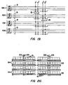
- each tile 40 has three global lines 81 running horizontally through it. The top two lines are connected to two of the possible four global wires. These horizontal lines 81 are connectable to the X2 input terminals of two vertically adjacent tiles through programmable switches. That is, the X2 input terminal of the logic cell 10 containing the global lines 81 and the X2 input terminal of the logic cell 10 in the tile immediately below may be connected to the horizontal global lines 81 of the first tile. Similarly, the tile below has a similar set of horizontal global lines 81 which are connected to the other two of the four main global lines. These lines 81 are connectable to the X2 input terminal of the logic cell 10 of that tile 40, and connectable to the input terminal of the logic cell in the tile below.
- Fig. 18 illustrates how two vertically adjacent tiles are connectable to the top two lines of the horizontal global lines 81 by the darkened vertical wiring segment 82, one of the local vertical wiring segments 43.
- the bottom line of the horizontal global lines 81 is connectable to the X1 input terminal of the logic cell in that tile only.
- the global lines distribute signals through spines formed by vertical global lines 82 and 83, as shown in Fig. 19 .
- Each pair of vertical global lines 82 and 84 drives one pair, i.e., the top two lines, of the horizontal global lines 81 in alternate rows.
- the bottom line in the global lines 81 is connectable to any one of the four lines in the lines 81 and 84.
- the lines 81 extend horizontally on either side of the vertical global lines 82 and 84.
- Each of the set of vertical lines 82 and 84 with the horizontal extensions of the lines 81 cover a sector of the array of tiles.
- Fig. 20 This is shown in an example in Fig. 20 , in which the global lines are labelled with the suffix A on the left sector, and the suffix B on the right sector. This allows the global distribution of signals to be designed so that the required skew characteristics of the signals may be met.
Landscapes
- Physics & Mathematics (AREA)
- Mathematical Physics (AREA)
- Engineering & Computer Science (AREA)
- Computer Hardware Design (AREA)
- Computing Systems (AREA)
- General Engineering & Computer Science (AREA)
- Computer Networks & Wireless Communication (AREA)
- Logic Circuits (AREA)
- Design And Manufacture Of Integrated Circuits (AREA)
Claims (35)
- Integrierte Schaltung, die eine Mehrzahl von Logikzellen, Verbindungsleitungen und Schaltern aufweist, zum programmierbaren Verbinden der Logikzellen und der Verbindungsleitungen,
dadurch gekennzeichnet,
dass jede Logikzelle (10) umfasst:erste und zweite Übertragungsgatter (12, 13), wobei jedes Übertragungsgatter einen Eingangsknoten, Regel-/Steuer-Anschlüsse, welche mit einem ersten wahren oder invertierten Signal oder mit einem festen logischen Pegel programmierbar verbindbar sind, und einen Ausgangsknoten aufweist, der gemeinsam mit dem anderen Übertragungsgatter verbunden ist,wobei ein Eingangsknoten des ersten Übertragungsgatters mit einem festen logischen Pegel oder einem Ausgangssignal von der Logikzelle programmierbar verbindbar ist,
wobei ein Eingangsknoten des zweiten Übertragungsgatters mit einem zweiten wahren oder invertierten Signal oder mit einem festen logischen Pegel programmierbar verbindbar ist; und
ein Logikzellengatter (14), das eine Mehrzahl von Eingangsknoten aufweist, umfassend
einen ersten Eingangsknoten, der mit den gemeinsam verbundenen Ausgangsknoten des ersten und zweiten Übertragungsgatters (12, 13) verbunden ist,
einen zweiten Eingangsknoten, der mit einem dritten wahren oder invertierten Signal oder mit einem festen logischen Pegel programmierbar verbindbar ist, und
einen Ausgangsknoten zum Erzeugen des Ausgangssignals der Logikzelle;
wobei die Logikzellen (10) einzeln oder mehrere zusammen programmiert werden können, um Logik- oder Speicherfunktionen zum Konfigurieren der integrierten Schaltung bereit zu stellen,
dadurch gekennzeichnet,
dass die Schalter programmierbar sind,
wobei für jedes Übertragungsgatter, die Regel-/Steuer-Anschlüsse mit dem ersten wahren oder invertierten Signal oder mit dem festen logischen Pegel durch einen programmierbaren Schalter programmierbar verbindbar sind,
der Eingangsknoten des ersten Übertragungsgatters mit dem festen logischen Pegel oder dem Ausgangssignal von der Logikzelle durch einen programmierbaren Schalter programmierbar verbindbar ist,
der Eingangsknoten des zweiten Übertragungsgatters mit dem zweiten wahren oder invertierten Signal oder mit dem festen logischen Pegel durch einen programmierbaren Schalter programmierbar verbindbar ist und
der zweite Eingangsknoten der Logikzelle (14) mit dem dritten wahren oder invertierten Signal oder mit dem festen logischen Pegel durch einen programmierbaren Schalter programmierbar verbindbar ist. - Integrierte Schaltung nach Anspruch 1,
wobei der feste logische Pegel entweder einen logischen "1"- oder einen logischen "Null"-Spannungspegel umfasst. - Integrierte Schaltung nach Anspruch 2,
wobei der feste logische Pegel entweder einen ersten Spannungsversorgungspegel oder einen zweiten Spannungsversorgungspegel umfasst. - Integrierte Schaltung nach Anspruch 2,
wobei das Logikgatter (14) ein NAND Logikgatter umfasst. - Integrierte Schaltung nach Anspruch 4,
ferner umfassend ein Paar von Invertern (15, 16),
wobei jeder Inverter einen Eingangsknoten, der mit dem Ausgangsknoten des Logikgatters verbunden ist und einen Ausgangsknoten umfasst, der mit gesonderten Verbindungsleitungen verbunden ist. - Integrierte Schaltung nach einem der Ansprüche 1 bis 5,
wobei jedes der Übertragungsgatter (12, 13) einen NMOS Transistor und einen PMOS Transistor umfasst, wobei jeder Transistor eine erste Source/einen ersten Drain aufweist, die/der mit dem Eingangsknoten des Übertragungsgatters verbunden ist, und eine zweite Source/einen zweiten Drain aufweist, die/der mit dem Ausgangsknoten des Übertragungsgatters verbunden ist, und ein Gate aufweist, das einen Regel-/Steuer-Anschluss des Übertragungsgatters bildet. - Integrierte Schaltung nach Anspruch 6, ferner umfassend einen Inverter, der einen Eingangsknoten aufweist, der mit dem ersten wahren oder invertierten Signal oder mit einem festen logischen Pegel programmierbar verbindbar ist und einen Ausgangsknoten aufweist, der mit einem Gate eines NMOS Transistors des ersten Übertragungsgatters und mit einem Gate eines PMOS Transistors des zweiten Übertragungsgatters verbunden ist.
- Integrierte Schaltung nach einem der Ansprüche 1 bis 7,
wobei das erste wahre oder invertierte Signal ein Taktsignal umfasst. - Integrierte Schaltung nach einem der Ansprüche 1 bis 8,
wobei das zweite wahre oder invertierte Signal ein Datensignal umfasst. - Integrierte Schaltung nach einem der Ansprüche 1 bis 9,
wobei das dritte wahre oder invertierte Signal ein Setzen/Rücksetzen-Signal umfasst. - Integrierte Schaltung nach einem der Ansprüche 1 bis 10, welche eine Anordnung von Platten aufweist, wobei jede Platte umfasst:eine von der Mehrzahl der Logikzellen;eine Mehrzahl von den Verbindungsleitungen zwischen benachbarten Platten in der Anordnung;eine Mehrzahl von Schaltern zum programmierbaren Verbinden der Verbindungsleitungen und der Eingangs- und Ausgangsanschlüsse von der einen der Mehrzahl der Logikzellen;wobei die Verbindungsleitungen derart angeordnet sind, dass ein Ausgangsanschluss von der einen der Mehrzahl der Logikzellen mit jedem Eingangsanschluss einer Logikzelle in jeder benachbarten Platte eindeutig programmierbar verbindbar ist.
- Integrierte Schaltung nach Anspruch 11,
wobei der Ausgangsanschluss der Logikzelle mit jedem Eingangsanschluss einer Logikzelle in jeder benachbarten Platte, einschließlich sich selbst, eindeutig programmierbar verbindbar ist. - Integrierte Schaltung nach einem der Ansprüche 11 oder 12,
wobei der Ausgangsanschluss der Logikzelle mit jedem Eingangsanschluss einer Logikzelle in jeder benachbarten Platte mittels eines einzelnen Schalters eindeutig programmierbar verbindbar ist. - Integrierte Schaltung nach einem der Ansprüche 11 bis 13,
wobei jede Logikzelle von jeder Platte drei Eingangsanschlüsse umfasst. - Integrierte Schaltung nach einem der Ansprüche 11 bis 14,
wobei jede Logikzelle von jeder Platte einen Ausgangsanschluss umfasst. - Integrierte Schaltung nach einem der Ansprüche 11 bis 13,
wobei jede Logikzelle von jeder Platte drei Eingangsanschlüsse und einen Ausgangsanschluss umfasst; und
die Verbindungsleitungen umfassen:eine erste Gruppe von drei Verbindungsleitungen, die im Allgemeinen in einer ersten Richtung ausgerichtet sind, wobei jeder Logikzelle-Ausgangsanschluss mit einer aus der ersten Gruppe der Verbindungsleitungen verbunden ist;eine zweite Gruppe von neun Verbindungsleitungen, die im Allgemeinen in einer zweiten, zur ersten Richtung senkrechten Richtung ausgerichtet sind, wobei jede aus der zweiten Gruppe von Verbindungsleitungen jede aus der ersten Gruppe von Verbindungsleitungen schneidet und mit dieser programmierbar verbindbar ist, wobei jeder Logikzelle-Eingangsanschluss mit einer aus der zweiten Gruppe von Verbindungsleitungen verbunden ist. - Integrierte Schaltung nach einem der Ansprüche 11 bis 13,
wobei jede Logikzelle von jeder Platte drei Eingangsanschlüsse und einen Ausgangsanschluss umfasst; und
die Verbindungsleitungen umfassen:eine erste Gruppe von drei Verbindungsleitungen, die im Allgemeinen in einer ersten Richtung ausgerichtet sind, wobei jeder Logikzelle-Ausgangsanschluss mit jeder aus der ersten Gruppe der Verbindungsleitungen programmierbar verbindbar ist; undeine zweite Gruppe von neun Verbindungsleitungen, die im Allgemeinen in einer zweiten, zur ersten Richtung senkrechten Richtung ausgerichtet sind, wobei jede aus der zweiten Gruppe von Verbindungsleitungen jede aus der ersten Gruppe von Verbindungsleitungen schneidet und mit dieser programmierbar verbindbar ist, wobei jeder Logikzelle-Eingangsanschluss mit einer aus der zweiten Gruppe von Verbindungsleitungen verbunden ist. - Integrierte Schaltung nach einem der Ansprüche 11 bis 13,
wobei die Verbindungsleitungen umfassen:eine erste Gruppe von Verbindungsleitungen, die im Allgemeinen in einer ersten Richtung ausgerichtet sind, wobei jeder Logikzelle-Ausgangsanschluss mit einer aus der ersten Gruppe der Verbindungsleitungen verbunden ist;eine zweite Gruppe von Verbindungsleitungen, die im Allgemeinen in einer zweiten, zur ersten Richtung senkrechten Richtung ausgerichtet sind,wobei jede aus der zweiten Gruppe von Verbindungsleitungen jede aus der ersten Gruppe von Verbindungsleitungen schneidet und mit dieser programmierbar verbindbar ist, wobei jeder Logikzelle-Eingangsanschluss mit einer aus der zweiten Gruppe von Verbindungsleitungen verbunden ist. - Integrierte Schaltung nach einem der Ansprüche 11 bis 13,
wobei die Verbindungsleitungen umfassen:eine erste Gruppe von Verbindungsleitungen, die im Allgemeinen in einer ersten Richtung ausgerichtet sind, wobei jeder Logikzelle-Ausgangsanschluss mit einer von der ersten Gruppe der Verbindungsleitungen durch eine Tri-State-Steuerschaltung verbunden ist, so dass der Ausgangsanschluss mit der einen von der ersten Gruppe von Verbindungsleitung programmierbar verbindbar ist; undeine zweite Gruppe von Verbindungsleitungen, die im Allgemeinen in einer zweiten, zur ersten Richtung senkrechten Richtung ausgerichtet sind,wobei jede aus der zweiten Gruppe von Verbindungsleitungen jede aus der ersten Gruppe von Verbindungsleitungen schneidet und mit dieser programmierbar verbindbar ist, wobei jeder Logikzelle-Eingangsanschluss mit einer aus der zweiten Gruppe von Verbindungsleitungen verbunden ist. - Integrierte Schaltung nach Anspruch 11,
wobei die Verbindungsleitungen umfassen:eine erste Gruppe von Verbindungsleitungen, die im Allgemeinen in einer ersten Richtung ausgerichtet sind, wobei jeder Logikzelle-Ausgangsanschluss mit jeder aus der ersten Gruppe der Verbindungsleitungen programmierbar verbindbar ist;eine zweite Gruppe von Verbindungsleitungen, die im Allgemeinen in einer zweiten, zur ersten Richtung senkrechten Richtung ausgerichtet sind,wobei jede aus der zweiten Gruppe von Verbindungsleitungen jede aus der ersten Gruppe von Verbindungsleitungen schneidet und mit dieser programmierbar verbindbar ist, wobei jeder Logikzelle-Eingangsanschluss mit einer aus der zweiten Gruppe von Verbindungsleitungen verbunden ist. - Integrierte Schaltung nach einem der Ansprüche 1 bis 10, welche eine Anordnung von Platten aufweist, wobei jede Platte umfasst:eine von der Mehrzahl der Logikzellen;eine Mehrzahl von den Verbindungsleitungen; undeine Mehrzahl von Schaltern zum programmierbaren Verbinden der Verbindungsleitungen und der Eingangs- und Ausgangsanschlüsse der Logikzellen;eine erste Gruppe von den Verbindungsleitungen, die im Allgemeinen in einer ersten Richtung ausgerichtet sind, wobei jeder Logikzelle-Ausgangsanschluss mit jeder aus der ersten Gruppe der Verbindungsleitungen programmierbar verbindbar ist;eine zweite Gruppe von Verbindungsleitungen, die im Allgemeinen in einer zweiten, zur ersten Richtung senkrechten Richtung ausgerichtet sind,wobei jede aus der zweiten Gruppe von Verbindungsleitungen jede aus der ersten Gruppe von Verbindungsleitungen schneidet und mit dieser programmierbar verbindbar ist, wobei jeder Logikzelle-Eingangsanschluss mit jeder von der zweiten Gruppe von Verbindungsleitungen programmierbar verbindbar ist,
wobei jede aus der ersten Gruppe von Verbindungsleitungen in jeder Platte mit ihrer entsprechenden ersten Gruppe von Verbindungsleitungen in benachbarten Platten und mit einer nicht-entsprechenden ersten Gruppe von Verbindungsleitungen in benachbarten Platten programmierbar verbindbar ist,
und ferner jede Leitung der zweiten Gruppen von Verbindungsleitungen in jeder Platte mit ihrer entsprechenden Verbindungsleitung der zweiten Gruppe in benachbarten Platten und mit einer nicht-entsprechenden Verbindungsleitung der zweiten Gruppe in benachbarten Platten programmierbar verbindbar ist. - Integrierte Schaltung nach Anspruch 21,
wobei die Logikzelle von jeder Platte einen einzigen Ausgangsanschluss aufweist. - Integrierte Schaltung nach Anspruch 21,
wobei jede Verbindungsleitung durch eine Mehrzahl von Puffern durch benachbarte Platten hindurch programmierbar verbindbar ist. - Integrierte Schaltung nach Anspruch 23,
wobei die Puffer der Mehrzahl von Puffern entlang jeder Verbindungsleitung in benachbarten Platten eine vorbestimmte Anzahl an Platten voneinander beabstandet sind. - Integrierte Schaltung nach Anspruch 24,
wobei die Puffer der Mehrzahl von Puffern entlang der Verbindungsleitung in benachbarten Platten jeweils zwei Platten voneinander beabstandet sind. - Integrierte Schaltung nach Anspruch 24,
wobei Puffer der Mehrzahl von Puffern entlang der Verbindungsleitung der ersten Gruppe in benachbarten Platten jeweils fünf Platten voneinander beabstandet sind und Puffer der Mehrzahl von Puffern entlang der Verbindungsleitung der zweiten Gruppe in benachbarten Platten jeweils vier Platten voneinander beabstandet sind. - Integrierte Schaltung nach Anspruch 21,
wobei jeder Ausgangsanschluss der Logikzelle von jeder Platte mit jeder aus der ersten Gruppe von Verbindungsleitungen einer benachbarten Platte programmierbar verbindbar ist. - Integrierte Schaltung nach einem der Ansprüche 1 bis 10,
wobei die Logikzellen der Mehrzahl von Logikzellen in Reihen und Spalten angeordnet sind, wobei jede Logikzelle Eingangs- und Ausgangsanschlüsse aufweist,
wobei die integrierte Schaltung umfasst:erste Verbindungsleitungen, die durch die Anordnung parallel zu den Spalten verlaufen;zweite Verbindungsleitungen, die durch jede Reihe von Logikzellen senkrecht zu den ersten Verbindungsleitungen verlaufen und diese schneiden, wobei die zweiten Verbindungsleitungen in einer Reihe mit wenigstens einem der Eingangsanschlüsse von jeder Logikzelle in der Reihe und mit wenigstens einem der Eingangsanschlüsse von jeder Logikzelle in einer benachbarten Reihe programmierbar verbindbar sind;wobei die zweiten Verbindungsleitungen abwechselnd mit der ersten und zweiten Gruppe der ersten Verbindungsleitungen in abwechselnden Reihen der Logikzellen programmierbar verbindbar sind;
wobei jede Logikzelle mit jeder von den ersten Verbindungsleitungen durch den einen Eingangsanschluss programmierbar verbindbar ist. - Integrierte Schaltung nach Anspruch 28,
ferner umfassend dritte Verbindungsleitungen, die durch jede Reihe von den Logikzellen senkrecht zu den ersten Verbindungsleitungen verlaufen und diese schneiden, wobei die dritten Verbindungsleitungen in einer Reihe mit wenigstens einem zweiten Eingangsanschluss von jeder Logikzelle in der Reihe programmierbar verbindbar sind,
und mit jeder ersten Verbindungsleitung programmierbar verbindbar sind, wobei jede Logikzelle mit jeder Logikzelle durch den zweiten Eingangsanschluss mit jeder von den ersten Verbindungsleitungen programmierbar verbindbar ist. - Integrierte Schaltung nach Anspruch 28,
wobei die zweiten Verbindungsleitungen mit den ersten Verbindungsleitungen an Schnittstellen der ersten und zweiten Verbindungsleitungen programmierbar verbindbar sind,
wobei die zweiten Verbindungsleitungen in einer Reihe mit einer gleichen Anzahl von Logikzellen durch den einen Eingangsanschluss auf jeder Seite einer Schnittstelle mit den ersten Verbindungsleitungen programmierbar verbindbar sind. - Integrierte Schaltung nach Anspruch 28,
wobei eine Mehrzahl von Logikzellen, die in Reihen und Spalten angeordnet sind, einen Bereich von Logikzellen umfasst,
wobei die integrierte Schaltung eine Mehrzahl von den Bereichen umfasst, um eine Anordnung von Logikzellen zu bilden. - Integrierte Schaltung nach Anspruch 28,
wobei wenigstens eine der ersten Verbindungsleitungen Taktsignale überträgt. - Integrierte Schaltung nach Anspruch 32,
ferner umfassend eine Mehrzahl von leitenden Anschlussflecken,
wobei wenigstens einer der leitenden Anschlussflecken Taktsignale empfängt,
wobei die eine von den ersten Verbindungsleitungen mit dem einen leitenden Anschlussfleck verbunden ist, um die Taktsignale zu übertragen. - Integrierte Schaltung nach Anspruch 28,
wobei die ersten Verbindungsleitungen vier Leitungen umfassen und die zweiten Verbindungsleitungen zwei Leitungen in jeder Reihe von Logikzellen umfassen. - Integrierte Schaltung nach Anspruch 34,
wobei die dritten Verbindungsleitungen eine Leitung in jeder Reihe von Logikzellen umfassen.
Applications Claiming Priority (3)
| Application Number | Priority Date | Filing Date | Title |
|---|---|---|---|
| US418972 | 1995-04-07 | ||
| US08/418,972 US5594363A (en) | 1995-04-07 | 1995-04-07 | Logic cell and routing architecture in a field programmable gate array |
| PCT/US1996/003599 WO1996031950A1 (en) | 1995-04-07 | 1996-03-14 | Logic cell and routing architecture in a field programmable gate array |
Publications (3)
| Publication Number | Publication Date |
|---|---|
| EP0819340A1 EP0819340A1 (de) | 1998-01-21 |
| EP0819340A4 EP0819340A4 (de) | 2000-11-15 |
| EP0819340B1 true EP0819340B1 (de) | 2010-05-05 |
Family
ID=23660283
Family Applications (1)
| Application Number | Title | Priority Date | Filing Date |
|---|---|---|---|
| EP96908832A Expired - Lifetime EP0819340B1 (de) | 1995-04-07 | 1996-03-14 | Logische zelle und verbindungsarchitektur in einem benutzerprogrammierbaren logischen feld |
Country Status (7)
| Country | Link |
|---|---|
| US (1) | US5594363A (de) |
| EP (1) | EP0819340B1 (de) |
| JP (1) | JP3645572B2 (de) |
| AU (1) | AU5254396A (de) |
| DE (1) | DE69638182D1 (de) |
| TW (1) | TW314653B (de) |
| WO (1) | WO1996031950A1 (de) |
Families Citing this family (96)
| Publication number | Priority date | Publication date | Assignee | Title |
|---|---|---|---|---|
| US5477165A (en) | 1986-09-19 | 1995-12-19 | Actel Corporation | Programmable logic module and architecture for field programmable gate array device |
| US5367208A (en) | 1986-09-19 | 1994-11-22 | Actel Corporation | Reconfigurable programmable interconnect architecture |
| US5198705A (en) | 1990-05-11 | 1993-03-30 | Actel Corporation | Logic module with configurable combinational and sequential blocks |
| US5742181A (en) * | 1996-06-04 | 1998-04-21 | Hewlett-Packard Co. | FPGA with hierarchical interconnect structure and hyperlinks |
| US5838040A (en) * | 1997-03-31 | 1998-11-17 | Gatefield Corporation | Nonvolatile reprogrammable interconnect cell with FN tunneling in sense |
| US5936426A (en) | 1997-02-03 | 1999-08-10 | Actel Corporation | Logic function module for field programmable array |
| US6272655B1 (en) * | 1998-06-11 | 2001-08-07 | Actel Corporation | Method of reducing test time for NVM cell-based FPGA |
| US6407576B1 (en) | 1999-03-04 | 2002-06-18 | Altera Corporation | Interconnection and input/output resources for programmable logic integrated circuit devices |
| US6294926B1 (en) | 1999-07-16 | 2001-09-25 | Philips Electronics North America Corporation | Very fine-grain field programmable gate array architecture and circuitry |
| US6567290B2 (en) * | 2000-07-05 | 2003-05-20 | Mosaic Systems, Inc. | High-speed low-power semiconductor memory architecture |
| US6594810B1 (en) | 2001-10-04 | 2003-07-15 | M2000 | Reconfigurable integrated circuit with a scalable architecture |
| US7378867B1 (en) * | 2002-06-04 | 2008-05-27 | Actel Corporation | Field-programmable gate array low voltage differential signaling driver utilizing two complimentary output buffers |
| US6891394B1 (en) * | 2002-06-04 | 2005-05-10 | Actel Corporation | Field-programmable gate array low voltage differential signaling driver utilizing two complimentary output buffers |
| US7269814B1 (en) | 2002-10-08 | 2007-09-11 | Actel Corporation | Parallel programmable antifuse field programmable gate array device (FPGA) and a method for programming and testing an antifuse FPGA |
| US6885218B1 (en) * | 2002-10-08 | 2005-04-26 | Actel Corporation | Parallel programmable antifuse field programmable gate array device (FPGA) and a method for programming and testing an antifuse FPGA |
| US6946871B1 (en) * | 2002-12-18 | 2005-09-20 | Actel Corporation | Multi-level routing architecture in a field programmable gate array having transmitters and receivers |
| US7385420B1 (en) | 2002-12-27 | 2008-06-10 | Actel Corporation | Repeatable block producing a non-uniform routing architecture in a field programmable gate array having segmented tracks |
| US6891396B1 (en) | 2002-12-27 | 2005-05-10 | Actel Corporation | Repeatable block producing a non-uniform routing architecture in a field programmable gate array having segmented tracks |
| US6838902B1 (en) * | 2003-05-28 | 2005-01-04 | Actel Corporation | Synchronous first-in/first-out block memory for a field programmable gate array |
| US7385419B1 (en) | 2003-05-30 | 2008-06-10 | Actel Corporation | Dedicated input/output first in/first out module for a field programmable gate array |
| US7080344B2 (en) * | 2003-06-25 | 2006-07-18 | International Business Machines Corporation | Coding of FPGA and standard cell logic in a tiling structure |
| DE102004063926B4 (de) * | 2004-03-24 | 2017-10-19 | Infineon Technologies Ag | Konfigurierbare Treiberzelle eines logischen Zellenfeldes |
| JP4368722B2 (ja) * | 2004-03-31 | 2009-11-18 | Necエレクトロニクス株式会社 | 汎用ロジックセルを備えた半導体装置 |
| WO2005109646A1 (ja) * | 2004-05-12 | 2005-11-17 | National University Corporation Okayama University | 多次元のスイッチトポロジーを有する集積回路 |
| US7430137B2 (en) * | 2004-09-09 | 2008-09-30 | Actel Corporation | Non-volatile memory cells in a field programmable gate array |
| JP4487738B2 (ja) * | 2004-11-17 | 2010-06-23 | ソニー株式会社 | 半導体集積回路 |
| US7212030B1 (en) | 2004-12-31 | 2007-05-01 | Actel Corporation | Field programmable gate array long line routing network |
| US8010826B2 (en) * | 2005-09-13 | 2011-08-30 | Meta Systems | Reconfigurable circuit with redundant reconfigurable cluster(s) |
| US7478261B2 (en) * | 2005-09-13 | 2009-01-13 | M2000 | Reconfigurable circuit with redundant reconfigurable cluster(s) |
| US7275196B2 (en) | 2005-11-23 | 2007-09-25 | M2000 S.A. | Runtime reconfiguration of reconfigurable circuits |
| EP2048784A4 (de) | 2006-07-27 | 2010-10-27 | Panasonic Corp | Integrierte halbleiterschaltung, programmumsetzungsvorrichtung und abbildungsvorrichtung |
| US7701248B2 (en) * | 2008-04-10 | 2010-04-20 | Silicon Storage Technology, Inc. | Storage element for controlling a logic circuit, and a logic device having an array of such storage elements |
| US9601692B1 (en) | 2010-07-13 | 2017-03-21 | Crossbar, Inc. | Hetero-switching layer in a RRAM device and method |
| US8946046B1 (en) | 2012-05-02 | 2015-02-03 | Crossbar, Inc. | Guided path for forming a conductive filament in RRAM |
| US9012307B2 (en) * | 2010-07-13 | 2015-04-21 | Crossbar, Inc. | Two terminal resistive switching device structure and method of fabricating |
| US9570678B1 (en) | 2010-06-08 | 2017-02-14 | Crossbar, Inc. | Resistive RAM with preferental filament formation region and methods |
| US8441835B2 (en) | 2010-06-11 | 2013-05-14 | Crossbar, Inc. | Interface control for improved switching in RRAM |
| KR101883236B1 (ko) | 2010-06-11 | 2018-08-01 | 크로스바, 인크. | 메모리 디바이스를 위한 필러 구조 및 방법 |
| US8374018B2 (en) | 2010-07-09 | 2013-02-12 | Crossbar, Inc. | Resistive memory using SiGe material |
| US8947908B2 (en) | 2010-11-04 | 2015-02-03 | Crossbar, Inc. | Hetero-switching layer in a RRAM device and method |
| US8884261B2 (en) | 2010-08-23 | 2014-11-11 | Crossbar, Inc. | Device switching using layered device structure |
| US8168506B2 (en) | 2010-07-13 | 2012-05-01 | Crossbar, Inc. | On/off ratio for non-volatile memory device and method |
| US8569172B1 (en) | 2012-08-14 | 2013-10-29 | Crossbar, Inc. | Noble metal/non-noble metal electrode for RRAM applications |
| US8467227B1 (en) | 2010-11-04 | 2013-06-18 | Crossbar, Inc. | Hetero resistive switching material layer in RRAM device and method |
| US9401475B1 (en) | 2010-08-23 | 2016-07-26 | Crossbar, Inc. | Method for silver deposition for a non-volatile memory device |
| US8404553B2 (en) | 2010-08-23 | 2013-03-26 | Crossbar, Inc. | Disturb-resistant non-volatile memory device and method |
| US8492195B2 (en) | 2010-08-23 | 2013-07-23 | Crossbar, Inc. | Method for forming stackable non-volatile resistive switching memory devices |
| US8889521B1 (en) | 2012-09-14 | 2014-11-18 | Crossbar, Inc. | Method for silver deposition for a non-volatile memory device |
| US8558212B2 (en) | 2010-09-29 | 2013-10-15 | Crossbar, Inc. | Conductive path in switching material in a resistive random access memory device and control |
| US8391049B2 (en) | 2010-09-29 | 2013-03-05 | Crossbar, Inc. | Resistor structure for a non-volatile memory device and method |
| US8502185B2 (en) | 2011-05-31 | 2013-08-06 | Crossbar, Inc. | Switching device having a non-linear element |
| USRE46335E1 (en) | 2010-11-04 | 2017-03-07 | Crossbar, Inc. | Switching device having a non-linear element |
| US8088688B1 (en) | 2010-11-05 | 2012-01-03 | Crossbar, Inc. | p+ polysilicon material on aluminum for non-volatile memory device and method |
| US8930174B2 (en) | 2010-12-28 | 2015-01-06 | Crossbar, Inc. | Modeling technique for resistive random access memory (RRAM) cells |
| US8791010B1 (en) | 2010-12-31 | 2014-07-29 | Crossbar, Inc. | Silver interconnects for stacked non-volatile memory device and method |
| US8815696B1 (en) | 2010-12-31 | 2014-08-26 | Crossbar, Inc. | Disturb-resistant non-volatile memory device using via-fill and etchback technique |
| US9153623B1 (en) | 2010-12-31 | 2015-10-06 | Crossbar, Inc. | Thin film transistor steering element for a non-volatile memory device |
| US8450710B2 (en) | 2011-05-27 | 2013-05-28 | Crossbar, Inc. | Low temperature p+ silicon junction material for a non-volatile memory device |
| US8394670B2 (en) | 2011-05-31 | 2013-03-12 | Crossbar, Inc. | Vertical diodes for non-volatile memory device |
| US9620206B2 (en) | 2011-05-31 | 2017-04-11 | Crossbar, Inc. | Memory array architecture with two-terminal memory cells |
| US8619459B1 (en) | 2011-06-23 | 2013-12-31 | Crossbar, Inc. | High operating speed resistive random access memory |
| US9564587B1 (en) | 2011-06-30 | 2017-02-07 | Crossbar, Inc. | Three-dimensional two-terminal memory with enhanced electric field and segmented interconnects |
| US8659929B2 (en) | 2011-06-30 | 2014-02-25 | Crossbar, Inc. | Amorphous silicon RRAM with non-linear device and operation |
| US9627443B2 (en) | 2011-06-30 | 2017-04-18 | Crossbar, Inc. | Three-dimensional oblique two-terminal memory with enhanced electric field |
| US8946669B1 (en) | 2012-04-05 | 2015-02-03 | Crossbar, Inc. | Resistive memory device and fabrication methods |
| US9166163B2 (en) | 2011-06-30 | 2015-10-20 | Crossbar, Inc. | Sub-oxide interface layer for two-terminal memory |
| WO2013015776A1 (en) | 2011-07-22 | 2013-01-31 | Crossbar, Inc. | Seed layer for a p + silicon germanium material for a non-volatile memory device and method |
| US8674724B2 (en) | 2011-07-29 | 2014-03-18 | Crossbar, Inc. | Field programmable gate array utilizing two-terminal non-volatile memory |
| US10056907B1 (en) | 2011-07-29 | 2018-08-21 | Crossbar, Inc. | Field programmable gate array utilizing two-terminal non-volatile memory |
| US9729155B2 (en) | 2011-07-29 | 2017-08-08 | Crossbar, Inc. | Field programmable gate array utilizing two-terminal non-volatile memory |
| US8716098B1 (en) | 2012-03-09 | 2014-05-06 | Crossbar, Inc. | Selective removal method and structure of silver in resistive switching device for a non-volatile memory device |
| US9087576B1 (en) | 2012-03-29 | 2015-07-21 | Crossbar, Inc. | Low temperature fabrication method for a three-dimensional memory device and structure |
| US9685608B2 (en) | 2012-04-13 | 2017-06-20 | Crossbar, Inc. | Reduced diffusion in metal electrode for two-terminal memory |
| US8658476B1 (en) | 2012-04-20 | 2014-02-25 | Crossbar, Inc. | Low temperature P+ polycrystalline silicon material for non-volatile memory device |
| US8796658B1 (en) | 2012-05-07 | 2014-08-05 | Crossbar, Inc. | Filamentary based non-volatile resistive memory device and method |
| US8765566B2 (en) | 2012-05-10 | 2014-07-01 | Crossbar, Inc. | Line and space architecture for a non-volatile memory device |
| US9280810B2 (en) * | 2012-07-03 | 2016-03-08 | Fotonation Limited | Method and system for correcting a distorted input image |
| US8928730B2 (en) * | 2012-07-03 | 2015-01-06 | DigitalOptics Corporation Europe Limited | Method and system for correcting a distorted input image |
| US9741765B1 (en) | 2012-08-14 | 2017-08-22 | Crossbar, Inc. | Monolithically integrated resistive memory using integrated-circuit foundry compatible processes |
| US9583701B1 (en) | 2012-08-14 | 2017-02-28 | Crossbar, Inc. | Methods for fabricating resistive memory device switching material using ion implantation |
| US8946673B1 (en) | 2012-08-24 | 2015-02-03 | Crossbar, Inc. | Resistive switching device structure with improved data retention for non-volatile memory device and method |
| US9312483B2 (en) | 2012-09-24 | 2016-04-12 | Crossbar, Inc. | Electrode structure for a non-volatile memory device and method |
| US9576616B2 (en) | 2012-10-10 | 2017-02-21 | Crossbar, Inc. | Non-volatile memory with overwrite capability and low write amplification |
| US11068620B2 (en) | 2012-11-09 | 2021-07-20 | Crossbar, Inc. | Secure circuit integrated with memory layer |
| US8982647B2 (en) | 2012-11-14 | 2015-03-17 | Crossbar, Inc. | Resistive random access memory equalization and sensing |
| US9412790B1 (en) | 2012-12-04 | 2016-08-09 | Crossbar, Inc. | Scalable RRAM device architecture for a non-volatile memory device and method |
| US9406379B2 (en) | 2013-01-03 | 2016-08-02 | Crossbar, Inc. | Resistive random access memory with non-linear current-voltage relationship |
| US9112145B1 (en) | 2013-01-31 | 2015-08-18 | Crossbar, Inc. | Rectified switching of two-terminal memory via real time filament formation |
| US9324942B1 (en) | 2013-01-31 | 2016-04-26 | Crossbar, Inc. | Resistive memory cell with solid state diode |
| US8934280B1 (en) | 2013-02-06 | 2015-01-13 | Crossbar, Inc. | Capacitive discharge programming for two-terminal memory cells |
| US10290801B2 (en) | 2014-02-07 | 2019-05-14 | Crossbar, Inc. | Scalable silicon based resistive memory device |
| US9153531B1 (en) | 2014-02-27 | 2015-10-06 | Altera Corporation | Methods and apparatus for reducing crosstalk and twist region height in routing wires |
| US9564394B1 (en) | 2014-11-18 | 2017-02-07 | Altera Corporation | Methods and apparatus for reducing spatial overlap between routing wires |
| US10452585B2 (en) * | 2016-09-16 | 2019-10-22 | Hewlett Packard Enterprise Development Lp | Crossbar switch with pipeline delay registers |
| WO2019030899A1 (en) * | 2017-08-10 | 2019-02-14 | Nec Corporation | ROUTING NETWORK FOR RECONFIGURABLE CIRCUIT |
| CN109344541B (zh) * | 2018-10-31 | 2023-01-31 | 京微齐力(北京)科技有限公司 | 一种根据区域布线拥挤度判定布线方向的方法 |
Family Cites Families (15)
| Publication number | Priority date | Publication date | Assignee | Title |
|---|---|---|---|---|
| US4870302A (en) * | 1984-03-12 | 1989-09-26 | Xilinx, Inc. | Configurable electrical circuit having configurable logic elements and configurable interconnects |
| US4642487A (en) * | 1984-09-26 | 1987-02-10 | Xilinx, Inc. | Special interconnect for configurable logic array |
| US5477165A (en) * | 1986-09-19 | 1995-12-19 | Actel Corporation | Programmable logic module and architecture for field programmable gate array device |
| US5367208A (en) * | 1986-09-19 | 1994-11-22 | Actel Corporation | Reconfigurable programmable interconnect architecture |
| US4758745B1 (en) * | 1986-09-19 | 1994-11-15 | Actel Corp | User programmable integrated circuit interconnect architecture and test method |
| US5451887A (en) * | 1986-09-19 | 1995-09-19 | Actel Corporation | Programmable logic module and architecture for field programmable gate array device |
| US5185706A (en) * | 1989-08-15 | 1993-02-09 | Advanced Micro Devices, Inc. | Programmable gate array with logic cells having configurable output enable |
| US5212652A (en) * | 1989-08-15 | 1993-05-18 | Advanced Micro Devices, Inc. | Programmable gate array with improved interconnect structure |
| US5245227A (en) * | 1990-11-02 | 1993-09-14 | Atmel Corporation | Versatile programmable logic cell for use in configurable logic arrays |
| US5122685A (en) * | 1991-03-06 | 1992-06-16 | Quicklogic Corporation | Programmable application specific integrated circuit and logic cell therefor |
| US5338984A (en) * | 1991-08-29 | 1994-08-16 | National Semiconductor Corp. | Local and express diagonal busses in a configurable logic array |
| JPH06318864A (ja) * | 1993-05-07 | 1994-11-15 | Toshiba Corp | フィールドプログラマブルゲートアレイ |
| EP0647030A3 (de) | 1993-09-30 | 1995-11-08 | Texas Instruments Inc | Integrierte Schaltungsvorrichtungen. |
| US5504440A (en) * | 1994-01-27 | 1996-04-02 | Dyna Logic Corporation | High speed programmable logic architecture |
| US5465055A (en) | 1994-10-19 | 1995-11-07 | Crosspoint Solutions, Inc. | RAM-logic tile for field programmable gate arrays |
-
1995
- 1995-04-07 US US08/418,972 patent/US5594363A/en not_active Expired - Lifetime
-
1996
- 1996-03-14 EP EP96908832A patent/EP0819340B1/de not_active Expired - Lifetime
- 1996-03-14 WO PCT/US1996/003599 patent/WO1996031950A1/en not_active Ceased
- 1996-03-14 DE DE69638182T patent/DE69638182D1/de not_active Expired - Lifetime
- 1996-03-14 AU AU52543/96A patent/AU5254396A/en not_active Abandoned
- 1996-03-14 JP JP53030896A patent/JP3645572B2/ja not_active Expired - Fee Related
- 1996-08-19 TW TW085110177A patent/TW314653B/zh not_active IP Right Cessation
Also Published As
| Publication number | Publication date |
|---|---|
| JP3645572B2 (ja) | 2005-05-11 |
| EP0819340A1 (de) | 1998-01-21 |
| EP0819340A4 (de) | 2000-11-15 |
| AU5254396A (en) | 1996-10-23 |
| TW314653B (de) | 1997-09-01 |
| US5594363A (en) | 1997-01-14 |
| WO1996031950A1 (en) | 1996-10-10 |
| DE69638182D1 (de) | 2010-06-17 |
| JPH11503290A (ja) | 1999-03-23 |
Similar Documents
| Publication | Publication Date | Title |
|---|---|---|
| EP0819340B1 (de) | Logische zelle und verbindungsarchitektur in einem benutzerprogrammierbaren logischen feld | |
| WO1996031950A9 (en) | Logic cell and routing architecture in a field programmable gate array | |
| JP3684241B2 (ja) | スケーリング可能な多重レベル相互接続アーキテクチャ用のフロア・プラン | |
| US5371422A (en) | Programmable logic device having multiplexers and demultiplexers randomly connected to global conductors for interconnections between logic elements | |
| US5631578A (en) | Programmable array interconnect network | |
| US6137308A (en) | Programmable interconnect matrix architecture for complex programmable logic device | |
| JP3727065B2 (ja) | スケーリング可能な多重レベル相互接続アーキテクチャ | |
| US6838904B1 (en) | Enhanced CPLD macrocell module having selectable bypass of steering-based resource allocation | |
| US6069490A (en) | Routing architecture using a direct connect routing mesh | |
| US5652529A (en) | Programmable array clock/reset resource | |
| US5483178A (en) | Programmable logic device with logic block outputs coupled to adjacent logic block output multiplexers | |
| US20100308863A1 (en) | Architecture of Function Blocks and Wirings in a Structured ASIC and Configurable Driver Cell of a Logic Cell Zone | |
| JPH0926869A (ja) | プログラマブル・アレイ | |
| GB2279168A (en) | Configurable logic array | |
| US6424171B1 (en) | Base cell and two-dimensional array of base cells for programmable logic LSI | |
| JP3581152B2 (ja) | プログラム可能な論理回路用のアーキテクチャおよび相互接続機構 | |
| US6268743B1 (en) | Block symmetrization in a field programmable gate array | |
| US6370140B1 (en) | Programmable interconnect matrix architecture for complex programmable logic device | |
| US7557612B2 (en) | Block symmetrization in a field programmable gate array | |
| US6285212B1 (en) | Block connector splitting in logic block of a field programmable gate array | |
| US6861869B1 (en) | Block symmetrization in a field programmable gate array | |
| GB2315146A (en) | Programmable logic with segmented localized conductors | |
| GB2312308A (en) | Configurable logic array |
Legal Events
| Date | Code | Title | Description |
|---|---|---|---|
| PUAI | Public reference made under article 153(3) epc to a published international application that has entered the european phase |
Free format text: ORIGINAL CODE: 0009012 |
|
| 17P | Request for examination filed |
Effective date: 19971105 |
|
| AK | Designated contracting states |
Kind code of ref document: A1 Designated state(s): DE |
|
| RAP3 | Party data changed (applicant data changed or rights of an application transferred) |
Owner name: GATEFIELD CORPORATION |
|
| A4 | Supplementary search report drawn up and despatched |
Effective date: 20001004 |
|
| AK | Designated contracting states |
Kind code of ref document: A4 Designated state(s): DE |
|
| 17Q | First examination report despatched |
Effective date: 20010206 |
|
| 17Q | First examination report despatched |
Effective date: 20010206 |
|
| GRAP | Despatch of communication of intention to grant a patent |
Free format text: ORIGINAL CODE: EPIDOSNIGR1 |
|
| GRAS | Grant fee paid |
Free format text: ORIGINAL CODE: EPIDOSNIGR3 |
|
| RAP1 | Party data changed (applicant data changed or rights of an application transferred) |
Owner name: ACTEL CORPORATION |
|
| GRAA | (expected) grant |
Free format text: ORIGINAL CODE: 0009210 |
|
| AK | Designated contracting states |
Kind code of ref document: B1 Designated state(s): DE |
|
| REF | Corresponds to: |
Ref document number: 69638182 Country of ref document: DE Date of ref document: 20100617 Kind code of ref document: P |
|
| PLBE | No opposition filed within time limit |
Free format text: ORIGINAL CODE: 0009261 |
|
| STAA | Information on the status of an ep patent application or granted ep patent |
Free format text: STATUS: NO OPPOSITION FILED WITHIN TIME LIMIT |
|
| 26N | No opposition filed |
Effective date: 20110208 |
|
| REG | Reference to a national code |
Ref country code: DE Ref legal event code: R097 Ref document number: 69638182 Country of ref document: DE Effective date: 20110207 |
|
| PG25 | Lapsed in a contracting state [announced via postgrant information from national office to epo] |
Ref country code: DE Free format text: LAPSE BECAUSE OF NON-PAYMENT OF DUE FEES Effective date: 20111001 |
|
| REG | Reference to a national code |
Ref country code: DE Ref legal event code: R119 Ref document number: 69638182 Country of ref document: DE Effective date: 20111001 |