EP0776088B1 - Etage de sortie d'amplificateur - Google Patents
Etage de sortie d'amplificateur Download PDFInfo
- Publication number
- EP0776088B1 EP0776088B1 EP97101192A EP97101192A EP0776088B1 EP 0776088 B1 EP0776088 B1 EP 0776088B1 EP 97101192 A EP97101192 A EP 97101192A EP 97101192 A EP97101192 A EP 97101192A EP 0776088 B1 EP0776088 B1 EP 0776088B1
- Authority
- EP
- European Patent Office
- Prior art keywords
- coupled
- current conducting
- amplifier
- fets
- conducting path
- Prior art date
- Legal status (The legal status is an assumption and is not a legal conclusion. Google has not performed a legal analysis and makes no representation as to the accuracy of the status listed.)
- Expired - Lifetime
Links
- 239000004020 conductor Substances 0.000 claims description 10
- 239000011324 bead Substances 0.000 claims description 4
- 238000004519 manufacturing process Methods 0.000 claims description 4
- 230000005669 field effect Effects 0.000 claims description 2
- 239000007787 solid Substances 0.000 claims description 2
- 239000003990 capacitor Substances 0.000 description 31
- 238000010586 diagram Methods 0.000 description 4
- 230000035699 permeability Effects 0.000 description 4
- 230000001105 regulatory effect Effects 0.000 description 4
- 230000037361 pathway Effects 0.000 description 2
- 239000004065 semiconductor Substances 0.000 description 2
- 239000000969 carrier Substances 0.000 description 1
- 230000008859 change Effects 0.000 description 1
- 238000004891 communication Methods 0.000 description 1
- 230000000295 complement effect Effects 0.000 description 1
- 230000001276 controlling effect Effects 0.000 description 1
- 238000013016 damping Methods 0.000 description 1
- 238000007599 discharging Methods 0.000 description 1
- 230000020169 heat generation Effects 0.000 description 1
- 239000000463 material Substances 0.000 description 1
- 239000002184 metal Substances 0.000 description 1
- 238000000034 method Methods 0.000 description 1
- 238000011084 recovery Methods 0.000 description 1
Images

Classifications
-
- H—ELECTRICITY
- H03—ELECTRONIC CIRCUITRY
- H03F—AMPLIFIERS
- H03F3/00—Amplifiers with only discharge tubes or only semiconductor devices as amplifying elements
- H03F3/20—Power amplifiers, e.g. Class B amplifiers, Class C amplifiers
- H03F3/21—Power amplifiers, e.g. Class B amplifiers, Class C amplifiers with semiconductor devices only
- H03F3/217—Class D power amplifiers; Switching amplifiers
- H03F3/2171—Class D power amplifiers; Switching amplifiers with field-effect devices
Definitions
- This invention related to improved amplifiers, especially Class D amplifiers. It is disclosed in the context of a class D audio amplifier.
- Class D amplifiers have many advantages such as small size, light weight, low cost, high efficiency, and reduced heat generation. However, undesirable radio frequency emissions can occur in the operation of such amplifiers. The emissions are a product of the rapid switching of substantial currents and voltages which are inherent in class D operation. These emissions can interfere with radio communication.
- a push-pull amplifier output stage comprising:
- uncontrolled current conducting paths are provided in antiparallel relation with both of the devices' controlled current conducting paths, and saturable reactors are provided in series with both of the uncontrolled current conducting paths to limit current flow therethrough during the switching of current flow from both of the controlled current conducting paths to both of the uncontrolled current conducting paths occasioned by operation of the amplifier.
- the devices are first and second field effect transistors (FETs), respectively.
- the first and second terminals are drain and source terminals of the FETS.
- the third terminals are gate terminals of the FETs.
- the source terminal of the first FET is coupled to the drain terminal of the second FET and to a load of the audio amplifier.
- the uncontrolled current conducting paths comprise first and second diodes.
- the anodes of the first and second diodes are coupled to the sources of the first and second FETs, respectively, and the cathodes of the first and second diodes are coupled to the drains of the first and second FETs, respectively.
- first and second diodes are first and second body diodes incorporated into the bodies of the first and second FETs, respectively, during manufacture of the first and second FETs.
- an RC circuit is situated in parallel with each of the diodes.
- the audio amplifier is a class D audio amplifier.
- the saturable reactor comprises a bead having a passageway therethrough for receiving a conductor which is in series with the uncontrolled current conducting path.
- class D amplifiers typically employ push-pull output stages.
- Each FET in a push-pull configuration of the illustrated type is actually a combination of an FET switch and a diode coupled in antiparallel relation.
- the switch which is closing is often trying to impress a reverse voltage across a forward-biased diode opposite the switch.
- Stored charge in the diode momentarily causes the diode to look like a short circuit, supporting a very large reverse "shoot-through” current until the charge is swept from the diode.
- the large current "snaps off” very quickly, transmitting radio frequency energy. This energy is a primary cause of undesirable radio frequency interference (RFI) which attends the operation of such circuits.
- RFID radio frequency interference
- the class D amplifier of Fig. 1 employs an ultra high permeability saturable reactor bead, such as the Toshiba AmobeadTM, on each switching MOSFET's drain lead. This places a saturable reactor in series with each switch/diode combination. In operation, during most of the switching cycle the ultra high permeability saturable reactors either are exposed to zero current or are in saturation and thus are not effectively in circuit.
- an ultra high permeability saturable reactor bead such as the Toshiba AmobeadTM
- this technique provides excellent RFI performance without shielded metal enclosures and feedthrough capacitors which previously have been used in class D audio amplifiers.
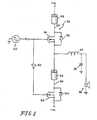
- a basic amplifier 32 receives appropriately preamplified and otherwise processed signals from a logic drive source 50.
- the driver stage of amplifier 32 includes a final driver inverting amplifier 52 and a pair of output MOSFET switches 54, 56.
- Switches 54, 56 illustratively are Motorola MTP 50N06E MOSFETs. Switches 54, 56 are coupled in push pull configuration, with the inverting amplifier 52 inverting the signal which is coupled to the gate of switch 54 and providing this inverted drive signal to the gate of switch 56.
- Each switch 54, 56 is provided with a body diode 58, 60, respectively.
- Diodes 58, 60 are formed on the material from which switches 54, 56 are fabricated at the time of fabrication of the switches 54, 56 so that devices 54, 58 are in the same package and devices 56, 60 are in the same package and there are no external leads between devices 54, 58 or between devices 56, 60.
- the drain lead of MOSFET 54 and cathode of diode 58 are coupled by a suitable conductor 62 to the +V, supply terminal.
- the source lead of MOSFET 54 and anode of diode 58 are coupled through the series inductor 34 to the parallel combination of capacitor 36 and load 38.
- the source lead of MOSFET 54 and anode of diode 58 are also coupled to the drain lead of MOSFET 56 and cathode of diode 60 by a suitable conductor 64.
- the source lead of MOSFET 56 and anode of diode 60 are coupled to the -V, supply terminal.
- a high magnetic permeability bead 66 is placed on each of conductors 62, 64.
- the various illustrated pin numbers on the illustrated integrated circuits and devices refer to the specific integrated circuits and devices which have already been identified or will be identified herein. However, that does not constitute a representation, nor should any such representation be inferred, that there are no integrated circuits or devices other than those identified herein that will perform the functions performed by the identified integrated circuits and devices.
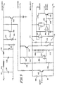
- V i Common mode noise rejection in the input signal V i is achieved by an input difference amplifier 80 which illustratively is one half of a National Semiconductor LM833.
- V i is coupled across the + and - input terminals of difference amplifier 80.
- Identical 10 K input resistors 12' are provided in series between the V i terminals and the respective + and - input terminals of amplifier 80.
- a feedback network including a parallel 22.1K resistor and a 47pF capacitor is coupled between the output terminal of amplifier 80 and its - input terminal.
- An identical parallel RC network is coupled between the + input terminal of amplifier 80 and the signal common.
- amplifier 80 and the signal common are coupled through identical 3.65K resistors to the - and + input terminals, respectively, of integrating difference amplifier 10.
- amplifier 10 illustratively is also half of an LM833 and illustratively is the other half of the same LM833 of which amplifier 80 is half. Consequently, +V s is illustrated connected to pin 8 of amplifier 80 and -V s , which in the illustrated embodiment is the chassis voltage of the circuit, is illustrated connected to pin 4 of amplifier 10. The remaining power supply connections to these amplifiers are made on the integrated circuit chip on which they are realized.
- a .0033 ⁇ F integrating capacitor 14 is coupled between the output terminal of amplifier 10 and its - input terminal.
- the + input terminal of amplifier 10 is coupled through a .0015 ⁇ F capacitor to the - input terminal of difference amplifier 16, and through a .0015 ⁇ F capacitor to the circuit common.
- the output terminal of amplifier 10 is coupled to the + input terminal of difference amplifier 16 and to the - input terminal of difference amplifier 18.
- the + input terminal of amplifier 18 is coupled to the circuit common.
- difference amplifiers 16, 18 are configured as a window comparator 22, and are realized on a National Semiconductor LM319 integrated circuit whose power supply terminals, pins 11 on the one hand and 3, 6 and 8 on the other, are coupled across the +V s and -V s (chassis) supply terminals.
- the output terminals 24 and 26, respectively, of amplifiers 16, 18 are coupled to the S and R input terminals, respectively, of SR flip flop 28.
- Flip flop 28 is realized by two, 84, 86, of the two-input NAND gates of an RCA CD4011B quad, two-input NAND gate integrated circuit. 3K pull up resistors couple the S and R input terminals, pins 6 and 1, respectively, of flip flop 28 to switched +V s .
- Pin 14 of flip flop 28 is also coupled to switched +V s .
- Pin 7 of flip flop 28 is coupled to -V s (chassis).
- NAND gate 84 is coupled to the remaining input terminal of NAND gate 86 and the output terminal of NAND gate 86 is coupled to the remaining input terminal of NAND gate 84. Both input terminals of each of the two remaining NAND gates on the CD4011B are coupled to -V s and their output terminals are left open.
- the drive for the output FETs is provided,by two identical output driver circuits 88, 90, only one of which will be described in further detail here.
- the Q output, pin 4, of flip flop 28 is coupled to the gate electrode of an FET 92, which illustratively is a type 2N7000 FET.
- the source of FET 92 is coupled to -V s and its drain is coupled through a 1K resistor to +3V s which is generated as will be described hereinafter.
- the drain of FET 92 is also coupled through an 82 ⁇ resistor to the joined bases of complementary NPN and PNP transistors 94, 96 which illustratively are types 2N4401 and 2N4403 transistors, respectively.
- the collector of transistor 94 is coupled to +3V s .
- the collector of transistor 96 is coupled to -V s .
- Their emitters are joined and form the output terminal 98 of driver circuit 88.
- the corresponding output terminal of driver circuit 90 is identified by the reference number 100.
- Each output transistor 54, 56 and its associated flyback diode 58,60, respectively, in the embodiment of Fig. 1 are realized in the embodiment of Fig. 2 by a pair of FETs 54-1, 54-2; 56-1, 56-2, respectively.
- the flyback diodes are incorporated into the FETs during the manufacture of the FETs.
- FETs 54-1 and 54-2 serve to provide a pathway for the charging of a .01 ⁇ F capacitor 102 in a first sense (source of FET 54-1 going more positive with respect to drain of FET 54-2) between the +V s and -V s terminals.
- FETs 56-1 and 56-2 serve to provide a pathway for discharging capacitor 102 in the first sense or charging it in a second, opposite sense (source of FET 56-2 going more positive with respect to drain of FET 56-1) between the +V s and -V s terminals.
- the drains of FETs 54-1 and 56-2 are coupled to +V s .
- the sources of FETs 54-2 and 56-1 are coupled to -V s .
- the source and drain, respectively, of FETs 54-1 and 56-1 are coupled through capacitor 102 and a series 1 ⁇ ring damping resistor 104 to the drain and source, respectively, of FETs 54-2 and 56-2, respectively.
- the gates of FETs 54-1 and 54-2 are coupled to terminal 100.
- FETs 56-1 and 56-2 are coupled to terminal 98.
- FETs 54-1, 54-2, 56-1 and 56-2 thus drive the voltage across capacitor 102 up and down between the +V s and -V s supply terminals based upon the switching voltages at the Q and Q terminals, pins 4 and 3, respectively, of flip flop 28.
- Feedback is provided from the source of FET 54-1 and the drain of FET 54-2 through 10K feedback resistors 39', 39' to the + and - input terminals, respectively, of amplifier 10.
- the speaker 38 and its associated circuitry 106 are coupled in parallel with the series RC combination 102, 104.
- the associated circuitry 106 includes a single turn saturable reactor 66 in series with the drain of each of FETs 54-2, 56-2. Reactors 66 are oriented in opposite senses so that, upon any change in current flow in circuit 106, the fields in reactors 66 cancel each other.
- a nine-turn inductor 34-1, 34-2 is in series between each reactor 66 and a respective terminal of speaker 38.
- a pair of .39 ⁇ F capacitors 36-1 and 36-2 in series are coupled across the speaker 38 terminals.
- a 2.2 ⁇ F capacitor 36-3 is coupled in parallel with series capacitors 36-1 and 36-2. The junction of capacitors 36-1 and 36-2 is coupled to the -V s terminal.
- Switching pulses appear across the RC series combination 102, 104 during operation, owing to the recovery of energy stored in the magnetic fields of inductors 34-1 and 34-2. These pulses are coupled through 18 ⁇ F, 35 VDC capacitors 114, 116 to a full wave diode bridge rectifier 117 which is coupled through a 20 ⁇ resistor to the switched +V s terminal. Rectifier 117 rectifies these pulses to provide a +3V s source. They are filtered and stored by a 120 ⁇ F, 35 VDC capacitor 118 from which +3V s is supplied to driver circuits 88, 90.
- a K 2 (V s + V i ) (V s - V i ) hysteresis generator 42 includes an operational transconductance amplifier 120 of, for example, a ROHM BA6110 integrated circuit 122.
- the I abc terminal, pin 4, of integrated circuit 122 is coupled through a 10K series resistor to the output terminal of amplifier 80 to receive the V i signal.
- V i is also coupled from the output terminal of amplifier 80 through a 10K series resistor to the + input terminal, pin 1, of integrated circuit 122.
- + V s is coupled through a 10K series resistor to the I d terminal, pin 3, of integrated circuit 122 and through the series combination of two forward biased diodes, illustratively type 1SS133 diodes, and a 10K series resistor to the - input terminal, pin 2, of integrated circuit 122.
- +V s is also coupled to pins 7 and 9 of integrated circuit 122.
- -V s is coupled to pin 5 of integrated circuit 122.
- Pin 6 the output terminal of operational transconductance amplifier 120, is coupled through a 15K resistor to the circuit common, through a 220pF capacitor to -V s (chassis), through a 300K resistor to +V s , and to the + input terminal of a difference amplifier 124 which is configured as a unity gain buffer amplifier. That is, the output terminal of amplifier 124 is coupled to its - input terminal. The output signal from amplifier 124 is coupled to the - input terminal of amplifier 16.
- Amplifier 124 illustratively is one fourth of a Motorola type MC34074 quad integrated circuit operational amplifier.
- Muting transistors are provided at appropriate locations throughout the circuit of Fig. 2. These include transistor 126, the collector and emitter of which are coupled across capacitor 14, and the base of which is coupled through a 10K resistor to a suitable source of muting signal. The presence of muting signal on the base of transistor 126 shorts the voltage across capacitor 14.
- the collector of a muting transistor 128 is coupled to the I abc terminal of operational transconductance amplifier 120.
- the base of transistor 128 is coupled through a 100K resistor to the muting signal source and through a .047 ⁇ F capacitor to -V s .
- the emitter of transistor 128 is also coupled to -V s .
- a muting signal on the base of transistor 128 shorts the I abc signal on pin 4 of the operational transconductance amplifier 120 to -V,.
- Transistors 126, 128 illustratively are type 2N3904 transistors.
- the collector of an additional muting transistor 130 is coupled through a suitable diode, illustratively a type 1SS133, to the drain terminal of FET 92 in each of driver circuits 88, 90.
- the emitter of transistor 130 is coupled to -V s .
- the base of transistor 130 is coupled through a 10K resistor to the muting signal source.
- the muting signal shorts the drive signal for transistors 94, 96 in each of circuits 88, 90 to -V s .
- Transistor 130 illustratively is a type 2N4401 transistor.
- a suitable power supply for the amplifier of Fig. 2 is illustrated in Fig. 3.
- a multiple section LC filter 132 is coupled across a 2V, source, such as a 12VDC vehicle battery. The more negative terminal of the source is denominated -V,.
- Filter 132 includes a .047 ⁇ F capacitor 134 across the source, a series 100 ⁇ H inductor 136 and 1500 ⁇ F, 16VDC capacitor 138 across capacitor 134, and a series 10 ⁇ H inductor 140 and 3000 ⁇ F, 16VDC capacitor 142 across capacitor 134.
- the voltage which appears at the common terminal of inductor 140 and capacitor 142 is denominated +V s .
- Overvoltage protection is provided by the series combination of a 1K resistor 144 and a zener diode 146 (illustratively a type 1N5246B) across the common terminal of inductor 140 and capacitor 142 and -V s .
- the junction of resistor 144 and zener diode 146 is coupled through a 1K resistor to the base of a PNP transistor 148.
- Transistor 148 illustratively is a type 2N3906.
- the emitter of transistor 148 is coupled to +V s and its collector is coupled to the base of a PNP transistor 150, illustratively a Motorola type MPS-A56.
- the emitter of transistor,150 is coupled to +V s .
- the base of transistor 150 is also coupled to +V s through a 2K resistor, and to the collector of an NPN transistor 152 through a 2K resistor.
- the emitter of transistor 152 is coupled to -V s .
- the base of transistor 152 is coupled through a 10K resistor to an on/off signal source.
- Transistor 152 illustratively is a Motorola type MPS-A06.
- the collector of transistor 150 forms the switched +V s supply.
- the collector of transistor 150 is coupled through series 33.2K and 68.1K resistors 156, 158, respectively, to -V s , the amplifier chassis.
- the common terminal of resistors 156, 158 is coupled to the - input terminal of a difference amplifier 160, the output terminal of which is coupled through a 680pF capacitor to its - input terminal to provide feedback thereto.
- Series 1K and 5.1K resistors 162, 164 respectively, couple the collector of transistor 150 to the output terminal of amplifier 160.
- the emitter of a transistor 166 (illustratively a type 2N4403) is coupled to the collector of transistor 150.
- the base of transistor 166 is coupled to the common terminal of resistors 162, 164.
- the collector of transistor 166 is coupled through a series voltage divider including a 120K resistor 165 and a 2.7K resistor 167 to -V s .
- the junction of resistors 165, 167 is coupled to the base of transistor 152.
- the collector of transistor 166 is also coupled through four series forward-biased diodes 168 (illustratively, type 1SS133s) and a 5.1K resistor 170 to - V s .
- the common terminal of diodes 168 and resistor 170 is coupled to the + input terminal of amplifier 160.
- the collector of transistor 166 forms the regulated +V s terminal of the supply of Fig. 3.
- Identical parallel RC networks 171 each including a 10K resistor 172 and a .047 ⁇ F capacitor 174, are coupled in series across the regulated +V s and -V s terminals.
- the common terminal of these two RC networks 171 is coupled to the + input terminal of a difference amplifier 176.
- Networks 171 divide in half the +V s to -V s voltage. This voltage is buffered by amplifier 176, which is configured as a unity gain amplifier, to provide at the output terminal of amplifier 176 the signal common for the circuits of Figs. 2-3.
- the muting signals for transistors 126, 128 and 130 of Fig. 2 are developed from the regulated +V s supply through a series RC time constant circuit including 4.7M resistor 180 and a .33 ⁇ F capacitor 182.
- This series circuit is coupled across the regulated +V s and -V s terminals, and the common terminal of resistor 180 and capacitor 182 is coupled to the + input terminal of a difference amplifier 184.
- Signal common is coupled to the - input terminal of amplifier 184.
- the output terminal of amplifier 184 is coupled through a series resistive voltage divider including a 10K resistor 186 and a 1K resistor 188 to -V s .
- the common terminal of resistors 186, 188 is coupled to the base of an NPN transistor 190, which illustratively is a type 2N3904.
- the emitter of transistor 190 is coupled to -V s .
- the muting signal is formed on the collector of transistor 190, which is coupled to the +3V s supply (Fig. 2) through a 5.1K resistor.
- Amplifiers 160, 176 and 184 illustratively are three fourths of the Motorola type MC34074 quad operational amplifier integrated circuit from which buffer amplifier 124 (Fig. 2) was realized.
Landscapes
- Engineering & Computer Science (AREA)
- Power Engineering (AREA)
- Amplifiers (AREA)
Claims (9)
- Etage (32) de sortie d'un amplificateur push-pull comprenant :un premier et un deuxième dispositifs (54, 56) à semiconducteur, ayant chacun un trajet de conduction de courant commandé comprenant une première et une deuxième bornes et un trajet de conduction de courant de commande comprenant au moins une troisième borne ;un premier trajet (58 ; 60) de conduction de courant non commandé en montage anti-parallèle avec l'un desdits trajets de conduction de courant commandé des dispositifs ; etun composant réactif (66) ; caractérisé en ce queledit étage de sortie est un étage de sortie d'amplificateur audio ; et en ce queledit composant réactif est un composant de réaction saturable (66) en série avec ledit premier trajet (58 ; 60) de conduction de courant non commandé pour limiter la circulation de courant dans celui-ci au cours de la commutation de la circulation de courant entre le trajet de conduction de courant commandé de l'un (54 ; 56) desdits dispositifs et ledit premier trajet (58 ; 60) de conduction de courant non commandé, provoquée par le fonctionnement dudit amplificateur (32), ledit composant réactif saturable arrivant à saturation et hors saturation au cours du fonctionnement dudit amplificateur.
- Appareil selon la revendication 1, comprenant en outre un deuxième trajet (58 ; 60) de conduction de courant non commandé en montage anti-parallèle avec l'autre des trajets de conduction de courant commandé des dispositifs.
- Appareil selon la revendication 2, comprenant en outre un deuxième composant réactif saturable (66) en série avec lesdits deuxièmes trajets (58 ; 60) de conduction de courant non commandés pour limiter la circulation de courant dans ceux-ci au cours de la commutation de circulation de courant entre le trajet de conduction de courant commandé de l'autre desdits dispositifs et ledit trajet (58 ; 60) de conduction de courant non commandé, provoquée par le fonctionnement dudit amplificateur (32).
- Apppareil selon l'une quelconque des revendications précédentes, caractérisé en outre en ce qu'il comprend un circuit RC (102, 104) en parallèle avec le ou les deux trajets de conduction (58, 60) non commandé(s).
- Appareil selon l'une quelconque des revendications précédentes, caractérisé en outre en ce que l'un ou les deux des dispositifs (54, 56) comprend (comprennent) des transistors à effet de champ (FET), les première et deuxième bornes sont des bornes de drain et de source du ou des FET (54, 56), la troisième ou les troisièmes borne(s) est ou sont une borne de grille ou des bornes de grille du ou des FET (54, 56), et la borne de source du premier FET (54) est couplée à la borne de drain du deuxième FET (56), s'il est présent, et à une charge (34, 36, 38) de l'amplificateur audio.
- Appareil selon la revendication 5, caractérisé en outre en ce que le trajet ou les trajets de conduction de courant non commandé(s) (58, 60) comprend ou comprennent une première (58) et, si elle existe, une deuxième (60) diodes, dont l'anode ou les anodes est ou sont couplée(s) à la source ou aux sources du premier et, s'il existe, du deuxième FET (54, 56), respectivement, et dont la cathode ou les cathodes est ou sont couplée(s) au drain ou aux drains du premier et, s'il existe, et du deuxième FET (54, 56), respectivement.
- Appareil selon la revendication 6, caractérisé en outre en ce que la première et, si elle existe, la deuxième diodes (58, 60) sont une première et, si elle existe, une deuxième diodes (58, 60) de corps incorporées dans le ou les corps du premier et, s'il existe, du deuxième FET (54, 56), respectivement, au cours de la fabrication du premier et, s'il existe, du deuxième FET (54, 56).
- Appareil selon l'une quelconque des revendications précédentes, caractérisé en outre en ce que l'amplificateur audio (32) est un amplificateur audio classe D.
- Appareil selon l'une quelconque des revendications précédentes, caractérisé en outre en ce que le ou chaque composant réactif saturable (66) comprend une perle traversée par un passage pour recevoir un conducteur (62, 64), ce conducteur (62, 64) étant en série avec ledit trajet (58, 60) de conduction de courant non commandé.
Applications Claiming Priority (3)
| Application Number | Priority Date | Filing Date | Title |
|---|---|---|---|
| US837166 | 1992-02-18 | ||
| US07/837,166 US5160896A (en) | 1992-02-18 | 1992-02-18 | Class D amplifier |
| EP93301064A EP0557032B1 (fr) | 1992-02-18 | 1993-02-15 | Modulateur de durée d'impulsion pour amplificateur en classe D |
Related Parent Applications (2)
| Application Number | Title | Priority Date | Filing Date |
|---|---|---|---|
| EP93301064A Division EP0557032B1 (fr) | 1992-02-18 | 1993-02-15 | Modulateur de durée d'impulsion pour amplificateur en classe D |
| EP93301064.7 Division | 1993-02-15 |
Publications (3)
| Publication Number | Publication Date |
|---|---|
| EP0776088A2 EP0776088A2 (fr) | 1997-05-28 |
| EP0776088A3 EP0776088A3 (fr) | 1997-08-06 |
| EP0776088B1 true EP0776088B1 (fr) | 2001-06-13 |
Family
ID=25273699
Family Applications (2)
| Application Number | Title | Priority Date | Filing Date |
|---|---|---|---|
| EP97101192A Expired - Lifetime EP0776088B1 (fr) | 1992-02-18 | 1993-02-15 | Etage de sortie d'amplificateur |
| EP93301064A Expired - Lifetime EP0557032B1 (fr) | 1992-02-18 | 1993-02-15 | Modulateur de durée d'impulsion pour amplificateur en classe D |
Family Applications After (1)
| Application Number | Title | Priority Date | Filing Date |
|---|---|---|---|
| EP93301064A Expired - Lifetime EP0557032B1 (fr) | 1992-02-18 | 1993-02-15 | Modulateur de durée d'impulsion pour amplificateur en classe D |
Country Status (5)
| Country | Link |
|---|---|
| US (1) | US5160896A (fr) |
| EP (2) | EP0776088B1 (fr) |
| JP (2) | JP3366677B2 (fr) |
| DE (2) | DE69330355T2 (fr) |
| DK (1) | DK0776088T3 (fr) |
Families Citing this family (57)
| Publication number | Priority date | Publication date | Assignee | Title |
|---|---|---|---|---|
| FR2686759B1 (fr) * | 1992-01-29 | 1994-04-22 | Sgs Thomson Microelectronics | Dispositif de regulation de puissance pour un haut-parleur de poste de telephone pendant une sonnerie . |
| DE4216203A1 (de) * | 1992-05-15 | 1993-11-18 | Sgs Thomson Microelectronics | Steuerschaltung |
| US5410592A (en) * | 1993-06-04 | 1995-04-25 | Harris Corporation | Class `D` audio speaker amplifier circuit with state variable feedback control |
| US5608401A (en) | 1994-12-28 | 1997-03-04 | Lucent Technologies Inc. | Three-level digital-to-analog converter for low-power consumption |
| US5594386A (en) * | 1995-04-21 | 1997-01-14 | Sipex Corporation | Pulse width modulated amplifier |
| TW437161B (en) * | 1995-08-30 | 2001-05-28 | Sony Corp | Audio signal amplifying apparatus |
| FR2743226B1 (fr) * | 1995-12-27 | 1998-03-20 | Sgs Thomson Microelectronics | Dispositif adaptatif a l'impedance d'une ligne d'alimentation |
| ATE213571T1 (de) * | 1996-05-31 | 2002-03-15 | Koninkl Philips Electronics Nv | Vorrichtung mit verstärker und sicherheitsmitteln sowie einem mit dem verstärker verbundenen filter |
| US5973368A (en) * | 1996-06-05 | 1999-10-26 | Pearce; Lawrence G. | Monolithic class D amplifier |
| US5767740A (en) * | 1996-09-27 | 1998-06-16 | Harris Corporation | Switching amplifier closed loop dual comparator modulation technique |
| US5963086A (en) * | 1997-08-08 | 1999-10-05 | Velodyne Acoustics, Inc. | Class D amplifier with switching control |
| EP0932932B1 (fr) * | 1997-08-12 | 2003-10-01 | Koninklijke Philips Electronics N.V. | Dispositif d'amplification de signaux numeriques |
| JP3550022B2 (ja) * | 1998-04-30 | 2004-08-04 | 松下電器産業株式会社 | D級増幅器を使用したシステム |
| US6107875A (en) * | 1998-10-15 | 2000-08-22 | Intersil Corporation | Variable frequency class D modulator with built in soft clipping and frequency limiting |
| US6587670B1 (en) * | 1998-12-22 | 2003-07-01 | Harris Corporation | Dual mode class D amplifiers |
| NL1011002C2 (nl) * | 1999-01-12 | 2000-07-20 | Univ Eindhoven Tech | Versterkerschakeling. |
| US6088251A (en) * | 1999-07-09 | 2000-07-11 | Fedan; Orest | Linearized duty radio, variable frequency switching regulator |
| US6304137B1 (en) * | 1999-12-23 | 2001-10-16 | Red Chip Company Limited | Output stage for high power class D amplifiers |
| US6441685B1 (en) | 2000-03-17 | 2002-08-27 | Jl Audio, Inc. | Amplifier circuit and method for providing negative feedback thereto |
| EP1293036B1 (fr) | 2000-05-25 | 2008-10-22 | Nxp B.V. | Filtre de demodulation |
| ES2296756T3 (es) * | 2000-05-25 | 2008-05-01 | Nxp B.V. | Arranque silencioso. |
| JP2003046345A (ja) * | 2001-07-27 | 2003-02-14 | Sony Corp | パワーアンプ装置 |
| CN1195353C (zh) * | 2001-12-03 | 2005-03-30 | 方虎堂 | 脉冲面积调制数字功率处理方法及装置 |
| PL198380B1 (pl) * | 2002-01-21 | 2008-06-30 | Adb Polska Sp | Wzmacniacz elektroakustyczny klasy D i sposób kompensacji wpływu napięcia zasilającego na wyjściowy sygnał użyteczny we wzmacniaczu elekroakustycznym klasy D |
| JP3499235B1 (ja) | 2002-08-28 | 2004-02-23 | 株式会社フライングモール | スイッチング回路及びディジタル電力増幅器 |
| US20080122534A1 (en) * | 2004-11-03 | 2008-05-29 | Bruce Halcro Candy | Amplifier Switching Output Stage With Low Distortion |
| EP1657815A1 (fr) * | 2004-11-12 | 2006-05-17 | Dialog Semiconductor GmbH | Méthode de stabilisation de la fréquence d'un modulateur auto-oscillant |
| US20060181346A1 (en) * | 2005-02-16 | 2006-08-17 | Nguyen Tranh T | Constant frequency self-oscillating amplifier |
| KR100617960B1 (ko) | 2005-02-24 | 2006-08-30 | 삼성전자주식회사 | 자가 발진형 펄스 폭 변조회로 및 펄스 폭 변조 방법 |
| JP2008536434A (ja) * | 2005-04-15 | 2008-09-04 | ボビナドス デ トランスフォルマドレス エセ エレ | D級増幅器 |
| US20090102550A1 (en) * | 2005-06-10 | 2009-04-23 | Rohm Co., Ltd. | Audio signal amplifier circuit with a mute function |
| US8050418B2 (en) * | 2005-07-07 | 2011-11-01 | Harman International Industries, Incorporated | Update system for an audio amplifier |
| US7262658B2 (en) * | 2005-07-29 | 2007-08-28 | Texas Instruments Incorporated | Class-D amplifier system |
| DE102005044710B4 (de) * | 2005-09-19 | 2011-07-07 | Conta GmbH, 45663 | Rückkopplungskorrektur für Schaltverstärker sowie eine Verwendung |
| US7400191B2 (en) | 2006-04-07 | 2008-07-15 | Manuel De Jesus Rodriguez | Switching power amplifier |
| JP4878227B2 (ja) * | 2006-06-27 | 2012-02-15 | 旭化成エレクトロニクス株式会社 | Pwm回路 |
| US7705672B1 (en) | 2007-02-12 | 2010-04-27 | Manuel De Jesus Rodriguez | Buck converters as power amplifier |
| JP4932573B2 (ja) * | 2007-04-09 | 2012-05-16 | ソニー・エリクソン・モバイルコミュニケーションズ株式会社 | オーディオ再生装置 |
| ATE532258T1 (de) * | 2007-05-07 | 2011-11-15 | Harman Int Ind | Automatische nullspannungschaltsteuerung |
| DE102008057234A1 (de) | 2007-12-14 | 2009-06-25 | Jens Kurrat | Aktivlautsprecher |
| EP2096753B1 (fr) * | 2008-02-29 | 2011-11-30 | STMicroelectronics (Grenoble) SAS | Amplificateur à commutation |
| US8731120B1 (en) * | 2011-04-08 | 2014-05-20 | Cameron M. Pike | Feedback-controlled biased inverting limiter for RFI suppression |
| US8410851B1 (en) | 2011-09-12 | 2013-04-02 | Wen-Hsiung Hsieh | Switching amplifier with an inductor |
| US8228118B1 (en) | 2011-09-17 | 2012-07-24 | Wen-Hsiung Hsieh | Switching amplifier using capacitor for transmitting energy |
| US8212613B1 (en) | 2011-09-21 | 2012-07-03 | Wen-Hsiung Hsieh | Switching amplifier using flyback transformer |
| US8451057B2 (en) | 2011-11-02 | 2013-05-28 | Wen-Hsiung Hsieh | Switching amplifier using inductor current feedback |
| JP6044269B2 (ja) | 2011-11-04 | 2016-12-14 | ヤマハ株式会社 | 自励発振型d級アンプおよび自励発振型d級アンプの自励発振周波数制御方法 |
| US9602067B2 (en) | 2011-11-15 | 2017-03-21 | Wen-Hsiung Hsieh | Switching amplifier with pulsed current supply |
| US8416020B1 (en) | 2011-11-20 | 2013-04-09 | Wen-Hsiung Hsieh | Switching amplifier and switching amplifying method |
| US8432221B1 (en) | 2011-11-27 | 2013-04-30 | Wen-Hsiung Hsieh | Switching amplifying method and switching amplifier |
| US8525587B2 (en) | 2011-12-04 | 2013-09-03 | Wen-Hsiung Hsieh | Switching amplifier with inductance means for transmitting energy |
| JP2013207534A (ja) * | 2012-03-28 | 2013-10-07 | Pioneer Electronic Corp | マルチチャンネルアンプ、マルチチャンネルアンプの制御方法およびプログラム |
| US8760230B2 (en) | 2012-06-28 | 2014-06-24 | Wen-Hsiung Hsieh | Switching amplifier with pulsed current source and sink |
| CN104348451A (zh) * | 2013-09-29 | 2015-02-11 | 深圳市伟创电气有限公司 | 迟滞性窗口比较器电路 |
| US9876422B2 (en) * | 2014-02-17 | 2018-01-23 | Trw Automotive U.S. Llc | RF noise reduction in switching mode power supplies |
| CN111373630B (zh) * | 2017-12-29 | 2022-03-22 | 威里利生命科学有限责任公司 | 用于无线功率发送器的高效功率放大器系统 |
| US10481193B2 (en) * | 2018-02-02 | 2019-11-19 | Texas Instruments Incorporated | Programmable load transient circuit |
Family Cites Families (12)
| Publication number | Priority date | Publication date | Assignee | Title |
|---|---|---|---|---|
| US2915588A (en) * | 1956-08-06 | 1959-12-01 | Amar G Bose | Pressure wave generation |
| US3038964A (en) * | 1956-08-06 | 1962-06-12 | Amar G Bose | Loudspeaker system |
| US3294981A (en) * | 1962-08-15 | 1966-12-27 | Bose Corp | Signal translation employing two-state techniques |
| US4456872A (en) * | 1969-10-27 | 1984-06-26 | Bose Corporation | Current controlled two-state modulation |
| GB2043370B (en) * | 1979-02-28 | 1983-03-09 | Chloride Group Ltd | Converters |
| US4516080A (en) * | 1982-04-01 | 1985-05-07 | Unisearch Limited | High-efficiency low distortion parallel amplifier |
| NL8203428A (nl) * | 1982-09-02 | 1984-04-02 | Philips Nv | Inrichting voor het omzetten van een elektrisch signaal in een akoestisch signaal. |
| JPS5967719A (ja) * | 1982-10-09 | 1984-04-17 | Nippon Gakki Seizo Kk | パルス幅変調回路 |
| US4602166A (en) * | 1983-05-19 | 1986-07-22 | Steve Smith | Transformer driving network with primary current limiting means |
| US4550359A (en) * | 1984-02-10 | 1985-10-29 | Honeywell Inc. | Voltage transient protection circuit for MOSFET power transistors |
| US4775841A (en) * | 1986-06-03 | 1988-10-04 | Trofimenkoff F N | Voltage to frequency conversion circuit with a pulse width to period ratio proportional to input voltage |
| DE4007564A1 (de) * | 1990-03-09 | 1991-09-12 | Siemens Ag | Leistungsverstaerker zur speisung induktiver lasten mit mos-feldeffekttransistoren |
-
1992
- 1992-02-18 US US07/837,166 patent/US5160896A/en not_active Expired - Lifetime
-
1993
- 1993-02-15 DK DK97101192T patent/DK0776088T3/da active
- 1993-02-15 DE DE69330355T patent/DE69330355T2/de not_active Expired - Lifetime
- 1993-02-15 EP EP97101192A patent/EP0776088B1/fr not_active Expired - Lifetime
- 1993-02-15 DE DE69318054T patent/DE69318054T2/de not_active Expired - Lifetime
- 1993-02-15 EP EP93301064A patent/EP0557032B1/fr not_active Expired - Lifetime
- 1993-02-18 JP JP02936393A patent/JP3366677B2/ja not_active Expired - Lifetime
-
2002
- 2002-08-23 JP JP2002243583A patent/JP3519723B2/ja not_active Expired - Lifetime
Non-Patent Citations (1)
| Title |
|---|
| HÄSSIG, H; ZOLLER, P: "Zuverläsiger Betrieb von MOSFETs in Brückenschaltungen", ELEKTRONIK, vol. 38, no. 10, 12 May 1989 (1989-05-12), MUNICH, pages 55 - 63, XP000071433 * |
Also Published As
| Publication number | Publication date |
|---|---|
| DK0776088T3 (da) | 2001-09-24 |
| JP3519723B2 (ja) | 2004-04-19 |
| DE69318054T2 (de) | 1998-08-13 |
| JP2003078363A (ja) | 2003-03-14 |
| DE69330355T2 (de) | 2001-09-20 |
| US5160896A (en) | 1992-11-03 |
| EP0557032A2 (fr) | 1993-08-25 |
| JPH06216664A (ja) | 1994-08-05 |
| EP0557032A3 (fr) | 1994-01-05 |
| JP3366677B2 (ja) | 2003-01-14 |
| EP0776088A3 (fr) | 1997-08-06 |
| DE69330355D1 (de) | 2001-07-19 |
| EP0776088A2 (fr) | 1997-05-28 |
| DE69318054D1 (de) | 1998-05-28 |
| EP0557032B1 (fr) | 1998-04-22 |
Similar Documents
| Publication | Publication Date | Title |
|---|---|---|
| EP0776088B1 (fr) | Etage de sortie d'amplificateur | |
| US4622482A (en) | Slew rate limited driver circuit which minimizes crossover distortion | |
| US4118731A (en) | Video amplifier with suppressed radio frequency radiation | |
| US6310508B1 (en) | High frequency switch | |
| US5374899A (en) | Self biased power amplifier employing FETs | |
| US6538514B2 (en) | Compensation method in a class-G amplifier output stage | |
| US5940498A (en) | Electronic voice circuit configuration | |
| EP0648010B1 (fr) | Circuit de compensation de fréquence pour stabiliser un amplificateur différentiel à transistors couplés en croix | |
| US4096443A (en) | Balanced source follower amplifier | |
| JP5064224B2 (ja) | デュアルバイアス制御回路 | |
| US5448311A (en) | Tri-state video differential driver | |
| US6982600B2 (en) | Class G-amplifiers | |
| US6664842B1 (en) | FET active load and current source | |
| US4719431A (en) | Audio power amplifier | |
| US4987392A (en) | Gallium arsenide antenna switch | |
| US5087890A (en) | Amplifier circuit | |
| JPH0964659A (ja) | 差動−シングルエンデッド・ビデオ母線受信装置 | |
| US3986131A (en) | Class AB-dual push-pull amplifier | |
| US5789982A (en) | Low distortion feedback IC amplifier and method | |
| JP2672731B2 (ja) | 電力増幅回路 | |
| US5760651A (en) | Inductorless voltage biasing circuit for and Ac-coupled amplifier | |
| US5166983A (en) | Mute circuit for audio amplifiers | |
| US4721921A (en) | Amplifier having improved gain/bandwidth product | |
| US6535064B2 (en) | Current-feedback amplifier exhibiting reduced distortion | |
| US4513251A (en) | Miller compensation for an operational amplifier |
Legal Events
| Date | Code | Title | Description |
|---|---|---|---|
| PUAI | Public reference made under article 153(3) epc to a published international application that has entered the european phase |
Free format text: ORIGINAL CODE: 0009012 |
|
| AC | Divisional application: reference to earlier application |
Ref document number: 557032 Country of ref document: EP |
|
| AK | Designated contracting states |
Kind code of ref document: A2 Designated state(s): DE DK FR GB IT SE |
|
| PUAL | Search report despatched |
Free format text: ORIGINAL CODE: 0009013 |
|
| AK | Designated contracting states |
Kind code of ref document: A3 Designated state(s): DE DK FR GB IT SE |
|
| 17P | Request for examination filed |
Effective date: 19971022 |
|
| 17Q | First examination report despatched |
Effective date: 19990429 |
|
| GRAG | Despatch of communication of intention to grant |
Free format text: ORIGINAL CODE: EPIDOS AGRA |
|
| GRAG | Despatch of communication of intention to grant |
Free format text: ORIGINAL CODE: EPIDOS AGRA |
|
| GRAG | Despatch of communication of intention to grant |
Free format text: ORIGINAL CODE: EPIDOS AGRA |
|
| GRAH | Despatch of communication of intention to grant a patent |
Free format text: ORIGINAL CODE: EPIDOS IGRA |
|
| GRAH | Despatch of communication of intention to grant a patent |
Free format text: ORIGINAL CODE: EPIDOS IGRA |
|
| GRAA | (expected) grant |
Free format text: ORIGINAL CODE: 0009210 |
|
| AC | Divisional application: reference to earlier application |
Ref document number: 557032 Country of ref document: EP |
|
| AK | Designated contracting states |
Kind code of ref document: B1 Designated state(s): DE DK FR GB IT SE |
|
| REF | Corresponds to: |
Ref document number: 69330355 Country of ref document: DE Date of ref document: 20010719 |
|
| ET | Fr: translation filed | ||
| ITF | It: translation for a ep patent filed | ||
| REG | Reference to a national code |
Ref country code: DK Ref legal event code: T3 |
|
| REG | Reference to a national code |
Ref country code: GB Ref legal event code: IF02 |
|
| PLBE | No opposition filed within time limit |
Free format text: ORIGINAL CODE: 0009261 |
|
| STAA | Information on the status of an ep patent application or granted ep patent |
Free format text: STATUS: NO OPPOSITION FILED WITHIN TIME LIMIT |
|
| 26N | No opposition filed | ||
| PGFP | Annual fee paid to national office [announced via postgrant information from national office to epo] |
Ref country code: FR Payment date: 20120306 Year of fee payment: 20 |
|
| PGFP | Annual fee paid to national office [announced via postgrant information from national office to epo] |
Ref country code: DE Payment date: 20120228 Year of fee payment: 20 |
|
| PGFP | Annual fee paid to national office [announced via postgrant information from national office to epo] |
Ref country code: IT Payment date: 20120224 Year of fee payment: 20 Ref country code: SE Payment date: 20120228 Year of fee payment: 20 Ref country code: GB Payment date: 20120224 Year of fee payment: 20 Ref country code: DK Payment date: 20120224 Year of fee payment: 20 |
|
| REG | Reference to a national code |
Ref country code: DE Ref legal event code: R071 Ref document number: 69330355 Country of ref document: DE |
|
| REG | Reference to a national code |
Ref country code: DK Ref legal event code: EUP |
|
| REG | Reference to a national code |
Ref country code: GB Ref legal event code: PE20 Expiry date: 20130214 |
|
| REG | Reference to a national code |
Ref country code: SE Ref legal event code: EUG |
|
| PG25 | Lapsed in a contracting state [announced via postgrant information from national office to epo] |
Ref country code: GB Free format text: LAPSE BECAUSE OF EXPIRATION OF PROTECTION Effective date: 20130214 Ref country code: DE Free format text: LAPSE BECAUSE OF EXPIRATION OF PROTECTION Effective date: 20130216 |