EP0753961B1 - Image processing apparatus using the same hardware during recording and reproduction - Google Patents
Image processing apparatus using the same hardware during recording and reproduction Download PDFInfo
- Publication number
- EP0753961B1 EP0753961B1 EP96305074A EP96305074A EP0753961B1 EP 0753961 B1 EP0753961 B1 EP 0753961B1 EP 96305074 A EP96305074 A EP 96305074A EP 96305074 A EP96305074 A EP 96305074A EP 0753961 B1 EP0753961 B1 EP 0753961B1
- Authority
- EP
- European Patent Office
- Prior art keywords
- image
- processing
- signal
- recording
- image signal
- Prior art date
- Legal status (The legal status is an assumption and is not a legal conclusion. Google has not performed a legal analysis and makes no representation as to the accuracy of the status listed.)
- Expired - Lifetime
Links
Images


Classifications
-
- H—ELECTRICITY
- H04—ELECTRIC COMMUNICATION TECHNIQUE
- H04N—PICTORIAL COMMUNICATION, e.g. TELEVISION
- H04N1/00—Scanning, transmission or reproduction of documents or the like, e.g. facsimile transmission; Details thereof
- H04N1/32—Circuits or arrangements for control or supervision between transmitter and receiver or between image input and image output device, e.g. between a still-image camera and its memory or between a still-image camera and a printer device
- H04N1/333—Mode signalling or mode changing; Handshaking therefor
-
- H—ELECTRICITY
- H04—ELECTRIC COMMUNICATION TECHNIQUE
- H04N—PICTORIAL COMMUNICATION, e.g. TELEVISION
- H04N23/00—Cameras or camera modules comprising electronic image sensors; Control thereof
- H04N23/80—Camera processing pipelines; Components thereof
-
- H—ELECTRICITY
- H04—ELECTRIC COMMUNICATION TECHNIQUE
- H04N—PICTORIAL COMMUNICATION, e.g. TELEVISION
- H04N2201/00—Indexing scheme relating to scanning, transmission or reproduction of documents or the like, and to details thereof
- H04N2201/32—Circuits or arrangements for control or supervision between transmitter and receiver or between image input and image output device, e.g. between a still-image camera and its memory or between a still-image camera and a printer device
- H04N2201/333—Mode signalling or mode changing; Handshaking therefor
- H04N2201/33307—Mode signalling or mode changing; Handshaking therefor of a particular mode
- H04N2201/33314—Mode signalling or mode changing; Handshaking therefor of a particular mode of reading or reproducing mode
- H04N2201/33328—Resolution
Definitions
- the present invention relates to an image processing apparatus and, more particularly, to pixel conversion processing of an image signal.
- a conventional image recording/reproduction apparatus comprises a recording unit for recording a video signal picked up by, e.g., a video camera on a recording medium such as a magnetic tape, and a reproduction unit for reproducing the video signal recorded by the recording unit.
- the video signal reproduced by the reproduction unit is converted in correspondence with a predetermined television system (e.g., NTSC system), and is output to an equipment such as a monitor.
- a predetermined television system e.g., NTSC system
- a video printer As a method of printing a video signal, a video printer is used.
- the video printer converts vertically elongated pixels of the NTSC system into square pixels by re-sampling the input analog image signal, stores image data consisting of the converted pixels in its internal frame memory having a predetermined capacity, performs image processing for the image data stored in the frame memory, and forms an image represented by the analog video signal on a transfer medium.
- the internal frame memory of the video printer has a capacity for, e.g., 640 ⁇ 480 pixels.
- a video printer having a digital I/F for receiving the digital video signal is used.
- the conventional image recording/reproduction apparatus does not execute any pixel conversion processing in correspondence with the characteristics of a destination equipment such as a video printer
- a means for executing the pixel conversion processing must be added, resulting in an increase in cost.
- the present invention has been made in consideration of the above situation and has as a concern to provide an image processing apparatus which can perform pixel conversion processing without increasing cost.
- United States Patent Specification No. US-A-4903132 discloses an electronic still camera capable of outputting, in different formats, image signals to a floppy disc, a printer, or to an NTSC system.
- an image processing apparatus as set out in claim 1 and method as set out in claim 7.
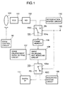
- Fig. 1 is a block diagram showing the arrangement of a digital image recording/reproduction apparatus according to an embodiment of the present invention.
- the digital image recording/reproduction apparatus comprises an optical system 100 which can perform a zoom operation, and a CCD (charge-coupled device) 101 for converting an object image caught by the optical system 100 into an electrical signal by photoelectric conversion.
- the maximum zoom ratio in the zoom operation of the optical system is set to be a predetermined value, e.g., ⁇ 12.
- the zoom ratio control is attained by a zoom control circuit 90.
- An electrical signal output from the CCD 101 is converted into digital image data by an A/D converter (to be referred to as "A/D" hereinafter) 102.
- the image data output from the A/D 102 is supplied to a selection switch 104.
- the selection switch 104 has two input terminals, i.e., REC and PB terminals, and one output terminal 104a.
- the REC terminal is connected to the output terminal of the A/D 102
- the PB terminal is connected to the output terminal of a reproduction system circuit 110 for reproducing image data recorded on a recording medium such as a magnetic tape.
- the output terminal 104a is connected to a frame memory 106.
- the frame memory 106 comprises a memory having a capacity for a predetermined number of pixels.
- the memory capacity is set to be 720 ⁇ 480 pixels with respect to image data corresponding to the NTSC system.
- Image data read out from the frame memory 106 is supplied to an image enlarging and reducing circuit 108.
- the image enlarging and reducing circuit 108 performs enlarging and reducing processing (i.e., electronic zoom processing) for the image data read out from the frame memory 106 in a recording operation mode, and performs pixel conversion processing for the image data read out from the frame memory 106 in a reproduction operation mode.
- enlarging and reducing processing i.e., electronic zoom processing
- image data to be output is one-frame image data having 720 ⁇ 480 pixels.
- the number of pixels of image data read out from the frame memory 106 is converted into that matching the equipment characteristics of a destination in accordance with the enlargement ratios set by the image enlargement ratio setting circuit 107, and the image data with the converted number of pixels is output.
- the image enlargement ratio setting circuit 107 sets the enlargement ratios for the enlarging and reducing processing or the pixel conversion processing of the image enlarging and reducing circuit 108 on the basis of externally input data.
- the enlargement ratios for the enlarging and reducing processing of the image enlarging and reducing circuit 108 are set in accordance with the zoom ratio set by a user's operation.
- the zoom ratio is set to be a value equal to or lower than the maximum zoom ratio ( ⁇ 12) of the zoom lens in the optical system
- a vertical enlargement ratio of ⁇ 1 and a horizontal enlargement ratio of ⁇ 1 are set as the enlargement ratios for the enlarging and reducing processing of the image enlarging and reducing circuit 108.
- the set zoom ratio equals that obtained by the zoom operation of the optical system.
- a zoom ratio x is set to be a value falling within the range from ⁇ 12 as the maximum zoom ratio of the zoom lens in the optical system to ⁇ 24
- the zoom ratio x is set to be ⁇ 24
- vertical and horizontal enlargement ratios of ⁇ 2 are respectively set as the enlargement ratios for the enlarging and reducing processing of the image enlarging and reducing circuit 108.
- the vertical and horizontal enlargement ratios are set, so that the number of pixels of image data read out from the frame memory 106 equals that corresponding to a destination equipment selected by the user.
- a table that stores the correspondence between destination equipments and their pixel sizes is stored in a storage device such as a ROM, and the destination equipment is selected on a menu screen to load the pixel size corresponding to the selected destination equipment, and the vertical and horizontal enlargement ratios are set on the basis of the loaded pixel size.
- Image data output from the image enlarging and reducing circuit is supplied to a selection switch 105.
- the selection switch 105 has one input terminal 105a and two output terminals, i.e., REC and PB terminals.
- the REC terminal is connected to the input terminal of a recording system circuit 109
- the PB terminal is connected to the input terminal of a digital I/F (interface) 111.
- the recording system circuit 109 digitally records image data input via the selection switch 105 on a recording medium such as a magnetic tape.
- the digital I/F 111 comprises an interface for supplying image data input via the selection switch 105 to a destination equipment, and its output terminal is connected to the destination equipment.
- the switching operations of the selection switches 104 and 105 are controlled on the basis of a control signal input from a control circuit (not shown) via an operation mode input terminal 103.
- the selection switches 104 and 105 respectively select the REC terminals on the basis of the control signal;
- the selection switches 104 and 105 respectively select the PB terminals on the basis of the control signal.
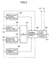
- Fig. 2 is a block diagram showing the arrangement of the image enlarging and reducing circuit arranged in the digital image recording/reproduction apparatus shown in Fig. 1.
- the image enlarging and reducing circuit 108 comprises input terminals 301 and 302 for respectively receiving the vertical and horizontal enlargement ratios set by the image enlargement ratio setting circuit 107.
- the vertical enlargement ratio input to the input terminal 301 is supplied to a vertical output size setting circuit 303, a reading start y address setting circuit 305, and an address conversion circuit 308.
- the horizontal enlargement ratio input to the input terminal 302 is supplied to a horizontal output size setting circuit 304, a reading start x address setting circuit 306, and the address conversion circuit 308.
- the vertical output size setting circuit 303 sets the vertical output size in the recording operation mode on the basis of equations (2) and (3) below:
- the horizontal output size setting circuit 304 sets the horizontal output size in the recording operation mode on the basis of equations (4) and (5) below:
- the reading start y address setting circuit 305 sets the reading start y address in the recording operation mode on the basis of equations (6) and (7) below:
- the reading start x address setting circuit 306 sets the reading start x address in the recording operation mode on the basis of equations (8) and (9) below:
- the vertical output size setting circuit 303, the reading start y address setting circuit 305, the horizontal output size setting circuit 304, and the reading start x address setting circuit 306 set data as indicated below in place of those set on the basis of equations (2) to (9) above.
- the following setting data are used for conversion from image data of the NTSC system into that of 640 ⁇ 480 pixels, and are set under the condition that the vertical enlargement ratio is set to be ⁇ 1, and the horizontal enlargement ratio is set to be ⁇ (640/720).
- the vertical and horizontal output sizes from the vertical and horizontal output size setting circuits 305 and 306 are supplied to an x,y counter 307.
- the x,y counter 307 incorporates x and y counters, and the counter values of these counters respectively indicate the x and y addresses of an image to be output.
- the values of the counters are set to be an initial value "0". While relationship that the counter value of the x counter is smaller than the horizontal output size is held, the count-up operation of the x counter is performed, and the counter values of the x and y counters are output. When relationship that the counter value of the x counter is equal to the horizontal output size is held, the counter value of the x counter is set to be "0", and the counter values of the x and y counters are output. When relationship that the counter value of the y counter is equal to the vertical output size is held, the counter value of the y counter is set to be "0", and the x and y counters are reset to the initial state.
- the counter values indicating the x and y addresses and supplied from the x,y counter 307 are supplied to the address conversion circuit 308.
- the address conversion circuit 308 receives the start y address supplied from the reading start y address setting circuit 305, the start x address supplied from the reading start x address setting circuit 306, and the vertical and horizontal enlargement ratios input to the input terminals 301 and 302, in addition to the counter values from the x,y counter 307.
- the address conversion circuit 308 converts x and y addresses indicated by the counter values supplied from the x,y counter 307 on the basis of the start y address supplied from the reading start y address setting circuit 305, the start x address supplied from the reading start x address setting circuit 306, and the vertical and horizontal enlargement ratios input to the input terminals 301 and 302, thereby calculating pixel addresses on the frame memory 106 corresponding to those of an output image.
- the calculated pixel addresses are supplied to a linear interpolation circuit 309.
- the linear interpolation circuit 309 outputs an address control signal from an output terminal 310 to the frame memory 106 on the basis of the input address data to load pixel data stored in the frame memory 106.
- Linear interpolation is performed based on the loaded pixel data, and pixel data obtained by the linear interpolation are output as output pixel data from an output terminal 312.
- Fig. 3 is a view of the pixel layout for explaining the operation of the image enlarging and reducing circuit arranged in the digital image recording/reproduction apparatus shown in Fig. 1.
- Fig. 3 illustrates image data of the NTSC system in the frame memory in correspondence with the pixel layout on the screen.
- the image enlarging and reducing circuit 108 reads out pixel data indicated by a hatched portion in Fig. 3 from the frame memory 106, performs enlarging processing (i.e., electronic zoom processing) at a predetermined zoom ratio, and outputs an image having a predetermined number of pixels, i.e., 720 ⁇ 480 pixels.
- enlarging processing i.e., electronic zoom processing
- the coordinate position of the upper left point of the hatched portion is calculated based on the start x and y addresses.
- the pixel conversion processing for converting image data of the NTSC system into that having pixels the number of which corresponds to the characteristics of a destination equipment is performed.
- the destination equipment is a video printer which incorporates a frame memory having a capacity for 640 ⁇ 480 pixels
- conversion from image data of the NTSC system into that having 640 ⁇ 480 pixels is performed under the condition that the vertical enlargement ratio is set to be ⁇ 1, and the horizontal enlargement ratio is set to be ⁇ (640/720), as described above.
- Figs. 4A and 4B are views of the pixel layout for explaining the operation of the address conversion circuit arranged in the image enlarging and reducing circuit shown in Fig. 2.
- Fig. 4A shows the pixel layout of image data of the NTSC system in the frame memory
- Fig. 4B shows the pixel layout of an image obtained by enlarging a hatched portion in Fig. 4A.
- Fig. 5 is a view of the pixel layout for explaining the operation of the linear interpolation circuit arranged in the image enlarging and reducing circuit shown in Fig. 2.
- a corresponding pixel P' has addresses (x', y') on the frame memory 106.
- the addresses are calculated based on equations (10) and (11) above.
- addresses are similarly calculated based on equations (10) and (11) above.
- the linear interpolation circuit 309 performs linear interpolation for specifying a corresponding pixel on the frame memory 106.
- linear interpolation circuit 309 in the recording or reproduction mode will be explained below. The following description will exemplify linear interpolation using four pixels, and the linear interpolation circuit 309 performs the same operation in both the recording and reproduction modes.
- dx represents the difference between the x addresses of the pixels P1 and P'
- dy represents the difference between the y addresses of the pixels P1 and P'. Note that the differences dx and dy respectively satisfy the following relations: 0 ⁇ dx ⁇ 1 0 ⁇ dy ⁇ 1
- the linear interpolation circuit 309 outputs addresses corresponding to the pixels P1, P2, P3, and P4 from the output terminal 310 to the frame memory 106, and fetches corresponding pixel data from an input terminal 311.
- Let p1', p2', p3', and p4' be the values of the fetched pixel data, and p' be the value of the pixel P'. Then, p' is calculated by equation (12) below: p' (1 - dx) ⁇ p1 ⁇ (1 - dy) + p3 ⁇ dy ⁇ + dx ⁇ p2 ⁇ (1 - dy) + p4 ⁇ dy ⁇
- the operation mode is set to be the recording mode.
- the selection switches 104 and 105 respectively select the REC terminals on the basis of a control signal from the control circuit.
- a zoom ratio is set by the user's operation, and the enlargement ratios for the enlarging and reducing processing of the image enlarging and reducing circuit 108 are set by the image enlargement ratio setting circuit 107 in correspondence with the zoom ratio.
- An electrical signal output from the CCD 101 is converted by the A/D 102 into image data, and the converted image data is stored in the frame memory 106 for each frame.
- the image data for one frame stored in the frame memory 106 is sequentially read out, and the readout image data is supplied to the image enlarging and reducing circuit 108.
- the image enlarging and reducing circuit 108 performs enlarging and reducing processing for the image data read out from the frame memory 106.
- the enlarging and reducing processing is executed in accordance with the enlargement ratios set by the image enlargement ratio setting circuit 107, i.e., electronic zoom processing is executed as needed, and image data having a predetermined number of pixels (e.g., 720 ⁇ 480 pixels) is output.
- the image data output from the image enlarging and reducing circuit 108 is supplied to the recording system circuit 109 via the selection switch 105 that selected the REC terminal, and the recording system circuit 109 digitally records the input image data on a recording medium such as a magnetic tape.
- the reproduction operation will be described below. The following description will exemplify a case wherein a reproduced image is printed by a video printer having a digital I/F and a frame memory for 640 ⁇ 480 pixels.
- the operation mode is set to be the reproduction mode. Upon setting this mode, the selection switches 104 and 105 respectively select the PB terminals on the basis of a control signal.
- the image enlargement ratio setting circuit 107 sets enlargement ratios for the pixel conversion processing of the image enlarging and reducing circuit 108.
- the enlargement ratios for the pixel conversion processing the vertical and horizontal enlargement ratios are set, so that the number of pixels of image data read out from the frame memory 106 equals that corresponding to the video printer selected by the user. More specifically, as described above, image data reproduced by the reproduction system circuit 110 is stored in the frame memory 110 for each frame. The image data for one frame stored in the frame memory 106 is sequentially read out, and the readout image data is supplied to the image enlarging and reducing circuit 108.
- the image enlarging and reducing circuit 108 performs pixel conversion processing for the image data read out from the frame memory 106.
- this pixel conversion processing the number of pixels of the image data read out from the frame memory 106 is converted into that (640 ⁇ 480) matching the video printer in correspondence with the enlargement ratios set by the image enlargement ratio setting circuit 107, and the image data with the converted number of pixels is output to the digital I/F 111 via the selection switch 105.
- the digital I/F 111 supplies the input image data to the video printer, and the video printer can form the input image data on a transfer medium without performing any pixel conversion processing for input image data.
- image enlarging and reducing circuit 108 has an arrangement common to the recording and reproduction modes, image enlarging processing (electronic zoom processing) and pixel conversion processing can be attained by a single circuit, thus constituting a low-cost recording/reproduction system.
- this embodiment has exemplified a digital image recording/reproduction apparatus.
- the present invention is not limited to the digital recording/reproduction apparatus.
- the present invention may be applied to an analog image recording/reproduction apparatus when the recording system circuit 109 shown in Fig. 1 performs D/A conversion processing for a digital image signal and records the converted signal on a recording medium, and the reproduction system circuit 110 performs A/D conversion processing for an analog image signal reproduced from the recording medium.
Applications Claiming Priority (3)
| Application Number | Priority Date | Filing Date | Title |
|---|---|---|---|
| JP19714095 | 1995-07-11 | ||
| JP19714095A JP3581443B2 (ja) | 1995-07-11 | 1995-07-11 | 画像処理装置及びその方法 |
| JP197140/95 | 1995-07-11 |
Publications (2)
| Publication Number | Publication Date |
|---|---|
| EP0753961A1 EP0753961A1 (en) | 1997-01-15 |
| EP0753961B1 true EP0753961B1 (en) | 2003-01-02 |
Family
ID=16369433
Family Applications (1)
| Application Number | Title | Priority Date | Filing Date |
|---|---|---|---|
| EP96305074A Expired - Lifetime EP0753961B1 (en) | 1995-07-11 | 1996-07-10 | Image processing apparatus using the same hardware during recording and reproduction |
Country Status (4)
| Country | Link |
|---|---|
| US (1) | US5960154A (ja) |
| EP (1) | EP0753961B1 (ja) |
| JP (1) | JP3581443B2 (ja) |
| DE (1) | DE69625553T2 (ja) |
Families Citing this family (8)
| Publication number | Priority date | Publication date | Assignee | Title |
|---|---|---|---|---|
| JP3700488B2 (ja) * | 1999-09-06 | 2005-09-28 | 日本ビクター株式会社 | 広角画像撮像装置 |
| JP3738652B2 (ja) * | 2000-03-24 | 2006-01-25 | コニカミノルタフォトイメージング株式会社 | デジタルカメラ |
| JP4593820B2 (ja) * | 2000-06-15 | 2010-12-08 | キヤノン株式会社 | 撮像装置、画像処理装置及び画像処理方法 |
| US6784941B1 (en) * | 2000-08-09 | 2004-08-31 | Sunplus Technology Co., Ltd. | Digital camera with video input |
| US7015422B2 (en) * | 2000-12-21 | 2006-03-21 | Mattson Technology, Inc. | System and process for heating semiconductor wafers by optimizing absorption of electromagnetic energy |
| JP2003209783A (ja) * | 2002-01-15 | 2003-07-25 | Canon Inc | ファイル送信装置およびファイル送信方法 |
| JP4165361B2 (ja) | 2003-10-07 | 2008-10-15 | ソニー株式会社 | 画像撮影装置、画像処理装置及びレンズ色収差補正方法 |
| US7522198B2 (en) * | 2005-04-20 | 2009-04-21 | Nokia Corporation | Electronic device, a method and a program product for determining a show zoom ratio for an image |
Family Cites Families (10)
| Publication number | Priority date | Publication date | Assignee | Title |
|---|---|---|---|---|
| JP2848396B2 (ja) * | 1987-09-26 | 1999-01-20 | 三菱電機株式会社 | 電子スチルカメラ |
| US5032918A (en) * | 1989-10-06 | 1991-07-16 | Nikon Corporation | Electronic still camera |
| DE69034198T2 (de) * | 1989-11-06 | 2006-04-20 | Canon K.K. | Elektronische Standbildkamera |
| US5268758A (en) * | 1990-09-26 | 1993-12-07 | Matsushita Electric Industrial Co., Ltd. | Horizontal line interpolation circuit and image pickup apparatus including it |
| JP2929749B2 (ja) * | 1991-04-05 | 1999-08-03 | 松下電器産業株式会社 | 画像伝送装置 |
| JP2806086B2 (ja) * | 1991-07-26 | 1998-09-30 | 松下電器産業株式会社 | 画像データ処理装置 |
| JPH05260352A (ja) * | 1992-03-11 | 1993-10-08 | Sony Corp | ビデオカメラ |
| BE1007211A5 (nl) * | 1993-06-10 | 1995-04-25 | Barco | Werkwijze en inrichting voor het converteren van een beeld. |
| JPH0795539A (ja) * | 1993-09-17 | 1995-04-07 | Canon Inc | 画像記録再生装置 |
| GB9325076D0 (en) * | 1993-12-07 | 1994-02-02 | The Technology Partnership Plc | Electronic camera |
-
1995
- 1995-07-11 JP JP19714095A patent/JP3581443B2/ja not_active Expired - Fee Related
-
1996
- 1996-07-02 US US08/675,403 patent/US5960154A/en not_active Expired - Lifetime
- 1996-07-10 EP EP96305074A patent/EP0753961B1/en not_active Expired - Lifetime
- 1996-07-10 DE DE69625553T patent/DE69625553T2/de not_active Expired - Lifetime
Also Published As
| Publication number | Publication date |
|---|---|
| US5960154A (en) | 1999-09-28 |
| DE69625553T2 (de) | 2003-10-02 |
| JPH0927943A (ja) | 1997-01-28 |
| JP3581443B2 (ja) | 2004-10-27 |
| EP0753961A1 (en) | 1997-01-15 |
| DE69625553D1 (de) | 2003-02-06 |
Similar Documents
| Publication | Publication Date | Title |
|---|---|---|
| CN100542249C (zh) | 摄影装置和显示控制方法 | |
| US7432958B2 (en) | Image pickup apparatus with function of adjusting incident light quantity | |
| US4651227A (en) | Video signal recording apparatus with A/D conversion | |
| US7142237B2 (en) | Imaging apparatus and processing method for converting the number of pixels of an input image | |
| US8564685B2 (en) | Video signal capturing apparatus, signal processing and control apparatus, and video signal capturing, video signal processing, and transferring system and method | |
| EP0753961B1 (en) | Image processing apparatus using the same hardware during recording and reproduction | |
| KR101154728B1 (ko) | 영상 신호 처리 장치 | |
| JP2620433B2 (ja) | 画像処理のためのフィールド補間回路及び方法 | |
| US5914755A (en) | Image transmission apparatus | |
| US5903703A (en) | Recording apparatus and reproduction apparatus storing data of a number of subframes | |
| JPH02268089A (ja) | 記録再生装置 | |
| JPH0837634A (ja) | 画像記録装置 | |
| US5625741A (en) | Video signal recording apparatus | |
| KR100220632B1 (ko) | 유니버설 시리얼 버스를 이용한 카메라 | |
| JP3214036B2 (ja) | 画像記録装置、画像再生装置および画像記録再生装置 | |
| EP1069781B1 (en) | Video signal recording and/or reproducing apparatus and methods, and image pickup apparatus | |
| JP3169397B2 (ja) | ディジタル電子スチル・カメラおよびその動作方法 | |
| KR100275903B1 (ko) | 정지화면을보면서동영상촬영기록이가능한디지털비디오캠코더 | |
| JP2000350079A (ja) | テレビジョンカメラ | |
| JP2877523B2 (ja) | 電子ビューファインダを有するビデオカメラ | |
| JPS6382066A (ja) | 電子ズ−ム機能付き撮像装置 | |
| EP0989746B1 (en) | Imaging apparatus having a high-speed imaging function with electronic zoom circuit | |
| KR100261592B1 (ko) | 고감도 전자 카메라 | |
| JP3822920B2 (ja) | ビデオ信号処理装置 | |
| JP2943546B2 (ja) | 画像記憶回路及びこれを用いた映像処理装置 |
Legal Events
| Date | Code | Title | Description |
|---|---|---|---|
| PUAI | Public reference made under article 153(3) epc to a published international application that has entered the european phase |
Free format text: ORIGINAL CODE: 0009012 |
|
| AK | Designated contracting states |
Kind code of ref document: A1 Designated state(s): DE FR GB NL |
|
| 17P | Request for examination filed |
Effective date: 19970528 |
|
| 17Q | First examination report despatched |
Effective date: 19990712 |
|
| GRAG | Despatch of communication of intention to grant |
Free format text: ORIGINAL CODE: EPIDOS AGRA |
|
| GRAH | Despatch of communication of intention to grant a patent |
Free format text: ORIGINAL CODE: EPIDOS IGRA |
|
| GRAA | (expected) grant |
Free format text: ORIGINAL CODE: 0009210 |
|
| AK | Designated contracting states |
Kind code of ref document: B1 Designated state(s): DE FR GB NL |
|
| REG | Reference to a national code |
Ref country code: GB Ref legal event code: FG4D Free format text: 20030102 |
|
| REF | Corresponds to: |
Ref document number: 69625553 Country of ref document: DE Date of ref document: 20030206 Kind code of ref document: P |
|
| ET | Fr: translation filed | ||
| PLBE | No opposition filed within time limit |
Free format text: ORIGINAL CODE: 0009261 |
|
| STAA | Information on the status of an ep patent application or granted ep patent |
Free format text: STATUS: NO OPPOSITION FILED WITHIN TIME LIMIT |
|
| 26N | No opposition filed |
Effective date: 20031003 |
|
| PGFP | Annual fee paid to national office [announced via postgrant information from national office to epo] |
Ref country code: DE Payment date: 20140731 Year of fee payment: 19 Ref country code: NL Payment date: 20140630 Year of fee payment: 19 |
|
| PGFP | Annual fee paid to national office [announced via postgrant information from national office to epo] |
Ref country code: GB Payment date: 20140724 Year of fee payment: 19 Ref country code: FR Payment date: 20140728 Year of fee payment: 19 |
|
| REG | Reference to a national code |
Ref country code: DE Ref legal event code: R119 Ref document number: 69625553 Country of ref document: DE |
|
| GBPC | Gb: european patent ceased through non-payment of renewal fee |
Effective date: 20150710 |
|
| REG | Reference to a national code |
Ref country code: NL Ref legal event code: MM Effective date: 20150801 |
|
| PG25 | Lapsed in a contracting state [announced via postgrant information from national office to epo] |
Ref country code: DE Free format text: LAPSE BECAUSE OF NON-PAYMENT OF DUE FEES Effective date: 20160202 Ref country code: GB Free format text: LAPSE BECAUSE OF NON-PAYMENT OF DUE FEES Effective date: 20150710 |
|
| REG | Reference to a national code |
Ref country code: FR Ref legal event code: ST Effective date: 20160331 |
|
| PG25 | Lapsed in a contracting state [announced via postgrant information from national office to epo] |
Ref country code: FR Free format text: LAPSE BECAUSE OF NON-PAYMENT OF DUE FEES Effective date: 20150731 Ref country code: NL Free format text: LAPSE BECAUSE OF NON-PAYMENT OF DUE FEES Effective date: 20150801 |