EP0750345A2 - Leistungs-Halbleitermodul - Google Patents
Leistungs-Halbleitermodul Download PDFInfo
- Publication number
- EP0750345A2 EP0750345A2 EP96109428A EP96109428A EP0750345A2 EP 0750345 A2 EP0750345 A2 EP 0750345A2 EP 96109428 A EP96109428 A EP 96109428A EP 96109428 A EP96109428 A EP 96109428A EP 0750345 A2 EP0750345 A2 EP 0750345A2
- Authority
- EP
- European Patent Office
- Prior art keywords
- power semiconductor
- semiconductor switches
- module according
- semiconductor module
- conductor tracks
- Prior art date
- Legal status (The legal status is an assumption and is not a legal conclusion. Google has not performed a legal analysis and makes no representation as to the accuracy of the status listed.)
- Granted
Links
Images

Classifications
-
- H—ELECTRICITY
- H10—SEMICONDUCTOR DEVICES; ELECTRIC SOLID-STATE DEVICES NOT OTHERWISE PROVIDED FOR
- H10W—GENERIC PACKAGES, INTERCONNECTIONS, CONNECTORS OR OTHER CONSTRUCTIONAL DETAILS OF DEVICES COVERED BY CLASS H10
- H10W90/00—Package configurations
-
- H—ELECTRICITY
- H10—SEMICONDUCTOR DEVICES; ELECTRIC SOLID-STATE DEVICES NOT OTHERWISE PROVIDED FOR
- H10W—GENERIC PACKAGES, INTERCONNECTIONS, CONNECTORS OR OTHER CONSTRUCTIONAL DETAILS OF DEVICES COVERED BY CLASS H10
- H10W72/00—Interconnections or connectors in packages
- H10W72/50—Bond wires
- H10W72/541—Dispositions of bond wires
- H10W72/5438—Dispositions of bond wires the bond wires having multiple connections on the same bond pad
-
- H—ELECTRICITY
- H10—SEMICONDUCTOR DEVICES; ELECTRIC SOLID-STATE DEVICES NOT OTHERWISE PROVIDED FOR
- H10W—GENERIC PACKAGES, INTERCONNECTIONS, CONNECTORS OR OTHER CONSTRUCTIONAL DETAILS OF DEVICES COVERED BY CLASS H10
- H10W72/00—Interconnections or connectors in packages
- H10W72/50—Bond wires
- H10W72/541—Dispositions of bond wires
- H10W72/547—Dispositions of multiple bond wires
- H10W72/5473—Dispositions of multiple bond wires multiple bond wires connected to a common bond pad
-
- H—ELECTRICITY
- H10—SEMICONDUCTOR DEVICES; ELECTRIC SOLID-STATE DEVICES NOT OTHERWISE PROVIDED FOR
- H10W—GENERIC PACKAGES, INTERCONNECTIONS, CONNECTORS OR OTHER CONSTRUCTIONAL DETAILS OF DEVICES COVERED BY CLASS H10
- H10W72/00—Interconnections or connectors in packages
- H10W72/50—Bond wires
- H10W72/541—Dispositions of bond wires
- H10W72/547—Dispositions of multiple bond wires
- H10W72/5475—Dispositions of multiple bond wires multiple bond wires connected to common bond pads at both ends of the wires
-
- H—ELECTRICITY
- H10—SEMICONDUCTOR DEVICES; ELECTRIC SOLID-STATE DEVICES NOT OTHERWISE PROVIDED FOR
- H10W—GENERIC PACKAGES, INTERCONNECTIONS, CONNECTORS OR OTHER CONSTRUCTIONAL DETAILS OF DEVICES COVERED BY CLASS H10
- H10W72/00—Interconnections or connectors in packages
- H10W72/90—Bond pads, in general
- H10W72/921—Structures or relative sizes of bond pads
- H10W72/926—Multiple bond pads having different sizes
-
- H—ELECTRICITY
- H10—SEMICONDUCTOR DEVICES; ELECTRIC SOLID-STATE DEVICES NOT OTHERWISE PROVIDED FOR
- H10W—GENERIC PACKAGES, INTERCONNECTIONS, CONNECTORS OR OTHER CONSTRUCTIONAL DETAILS OF DEVICES COVERED BY CLASS H10
- H10W90/00—Package configurations
- H10W90/701—Package configurations characterised by the relative positions of pads or connectors relative to package parts
- H10W90/751—Package configurations characterised by the relative positions of pads or connectors relative to package parts of bond wires
- H10W90/753—Package configurations characterised by the relative positions of pads or connectors relative to package parts of bond wires between laterally-adjacent chips
-
- H—ELECTRICITY
- H10—SEMICONDUCTOR DEVICES; ELECTRIC SOLID-STATE DEVICES NOT OTHERWISE PROVIDED FOR
- H10W—GENERIC PACKAGES, INTERCONNECTIONS, CONNECTORS OR OTHER CONSTRUCTIONAL DETAILS OF DEVICES COVERED BY CLASS H10
- H10W90/00—Package configurations
- H10W90/701—Package configurations characterised by the relative positions of pads or connectors relative to package parts
- H10W90/751—Package configurations characterised by the relative positions of pads or connectors relative to package parts of bond wires
- H10W90/754—Package configurations characterised by the relative positions of pads or connectors relative to package parts of bond wires between a chip and a stacked insulating package substrate, interposer or RDL
Definitions
- the invention relates to a power semiconductor module having a housing and a metal base, on which electrically insulating and thermally conductive substrates carrying interconnects are arranged, with six controllable power semiconductor switches located next to one another, each of which is electrically conductively attached to one of the interconnects , with load current connections which are connected to the housing wall and which have bonding surfaces on the underside inside the housing, which are electrically connected to the controllable power semiconductor switches via bonding wires.
- Such a power semiconductor module is on the market and is e.g. offered in the short catalog 1993/94 "SIPMOS semiconductors", page 35.
- As a power semiconductor switch it contains six IGBTs that are connected to form a three-phase converter bridge. The module has two DC connections and three AC connections. These connections carry the load current.
- the invention has for its object to develop a power semiconductor module of the type mentioned so that several circuit variants can be obtained only by changing the bond connections in the housing.
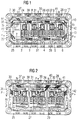
- the power semiconductor module according to FIG. 1 is designated by 10. It contains a metal base 12 with which an insulating frame 11 is attached.
- the insulating frame forms the walls of the module and carries all the load connections 13 to 21.
- a cover (not shown) is placed on the insulating frame, the frame and cover form the housing.
- Substrates 7, 8, 9 are attached to the floor 12. These consist, for example, of aluminum oxide Al 2 O 3 or aluminum nitride AlN. Its underside is provided with a metal layer over which the substrates with the bottom 12, for example by soldering are connected. The top of the substrates are provided with interconnects 24, 25; 26, 27; 28, 29 provided. These interconnects carry power semiconductor switches 1, 2; 3, 4; 5, 6.
- the semiconductor switches can be, for example, IGBTs (isolated gate bipolar transistors), each of which can have a freewheeling diode connected in anti-parallel. In the case of the power semiconductor switch 1, this diode is designated 45, in the other switches the designation of the diode has been omitted for the sake of clarity.
- the semiconductor switches can also be MOSFETs or consist of several semiconductor components connected in parallel.
- An additional interconnect 30, 31, 32 is assigned to two of the semiconductor switches lying next to one another.
- the additional interconnects are preferably between the interconnects of the semiconductor switches and at least one load connection. If the power semiconductor module has a cuboid shape, most of the load connections are arranged on the long side of the housing. In this case, these are the load connections 15, 16, 17, 18 and 19. Of which the load current connections 19, 17 and 15 are the AC output with the three phases U, V and W.
- the connections 20, 14 on the narrow sides of the housing are the negative DC voltage connections and connections 21, 13 the positive ones. However, it may also be sufficient to apply the DC voltage only to the load current connections 13, 14 or to 20, 21.
- the module is connected internally exclusively via bond connections.
- the load current connections 21 to 13 carry bonding surfaces 35, 36, 37, 38, 39, 40, 41, 42 and 43 at the lower end. These bonding surfaces protrude into the interior of the housing.
- the upper sides of the load connections are preferably designed as pins, via which the module can be connected to a circuit board by wave soldering.
- the load current of the module connected as a three-phase converter bridge is as follows: Connection 19 - bond area 37 - interconnect 24 - collector IGBT 2 - emitter IGBT 2 - interconnect 30 - bond area 36 - connection 20. In addition, current flows from connection 13/21 - interconnect 25 - collector IGBT 1 - emitter IGBT 1 - interconnect 24 - bond area 37 to the load connection 19.
- the electrical connections within the module are each represented by three bond wires for better clarity. With high currents, of course, more, e.g. 10 to 15 parallel bond wires are used. If such a bonding wire has a diameter of e.g. 400 ⁇ m, a three-phase converter bridge with e.g. Establish 3 x 120 A load current. The anti-parallel diodes form bond bases for the emitter sides of the IGBT.
- the power semiconductor module according to FIG. 2 has the same structure as the power semiconductor module according to FIG. 1.
- the designation of the semiconductor switch or IGBT has been omitted here for the sake of clarity.
- the load current connections and the interconnects and the bond areas have the same designation as in FIG. 1.
- the power semiconductor module according to FIG. 2 embodies three individual switches, in each of which the semiconductor switches 1 and 2, 3 and 4, 5 and 6 are made by bonding connections between the interconnects 24 and 25, 26 and 27, 28 and 29 and by bonding connections between two adjacent IGBTs 1, 2; 3, 4; 5, 6 and the respectively associated additional interconnect 30, 31, 32 are connected in parallel.
- the load connection 19 is the negative connection N- and the load connection 20 is the positive connection P +.
- the electrical connection goes from the load connection 19 to the load connection 20 via the bonding surface 37 - interconnect 30 - emitter IGBT 1 / IGBT 2 - interconnects 24/25 - bonding surface 36 - load connection 20.
- the load terminal 17 is the positive terminal P + and the terminal 16 is the negative terminal N-.
- the load connections 17 and 16 are connected via bond area 39 - interconnects 26/27 - collector IGBT 3 / IGBT 4 - emitter IGBT 3 / IGBT 4 - interconnect 31 - bond area 40 - load connection 16.
- the load connection 15 is the negative DC voltage connection N- and the load connection 14 is the positive DC voltage connection P +. Both are electrically connected via the bonding surface 41 - interconnect 32 - emitter IGBT 5 / IGBT 6 - collector IGBT 5 / IGBT 6 - interconnect 28 / interconnect 29 - bonding surface 42 - load connection 14.
- connections on the other long side of the modules are control connections, which are connected to the gate contacts and, if appropriate, to auxiliary emitter contacts of the IGBT via corresponding bonding surfaces.
- control connections which are connected to the gate contacts and, if appropriate, to auxiliary emitter contacts of the IGBT via corresponding bonding surfaces.
- the bond areas of these load connections must either be connectable to one of the additional interconnects or one of the interconnects provided with an IGBT. To do this, the additional interconnects must be directly opposite or laterally offset from the bond areas. On the long sides of the housing, the additional interconnects are preferably between the bond areas and the other interconnects.
- a bridge branch for triple load current is obtained by connecting the connections 15, 17, 19 to one another in the module according to FIG.
Landscapes
- Inverter Devices (AREA)
- Power Conversion In General (AREA)
Abstract
Description
- Die Erfindung bezieht sich auf ein Leistungs-Halbleitermodul mit einem Gehäuse und einem metallenen Boden, auf dem elektrisch isolierende und thermisch leitende, Leitbahnen tragende Substrate angeordnet sind, mit sechs nebeneinander liegenden steuerbaren Leistungs-Halbleiterschaltern, die jeweils auf einer der Leitbahnen elektrisch leitend befestigt sind, mit Laststromanschlüssen, die mit der Gehäusewand verbunden sind und die an der Unterseite im Inneren des Gehäuses Bondflächen haben, die über Bonddrähte elektrisch mit den steuerbaren Leistungs-Halbleiterschaltern verbunden sind.
- Ein solches Leistungs-Halbleitermodul ist auf dem Markt und wird z.B. im Kurzkatalog 1993/94 "SIPMOS-Halbleiter", Seite 35 angeboten. Es enthält als Leistungs-Halbleiterschalter sechs IGBT, die zu einer Dreiphasen-Stromrichterbrücke zusammengeschaltet sind. Das Modul hat zwei Gleichstromanschlüsse und drei Wechselstromanschlüsse. Diese Anschlüsse führen den Laststrom.
- Von Anwenderseite besteht oft der Wunsch, ein Leistungs-Halbleitermodul der beschriebenen Art z.B. in Form von drei Einzelschaltern für jeweils den doppelten Laststrom oder als Brückenzweig für den dreifachen Laststrom des Dreiphasen-Stromrichtermoduls zu betreiben. Dies erforderte bisher Änderungen des Layouts der Leiterbahnen.
- Der Erfindung liegt die Aufgabe zugrunde, ein Leistungs-Halbleitermodul der genannten Art so weiterzubilden, daß mehrere Schaltungsvarianten lediglich durch Änderungen der Bondverbindungen im Gehäuse erhalten werden können.
- Diese Aufgabe wird gelöst durch die Merkmale:
- a) Für je zwei der nebeneinander liegenden Leistungs-Halbleiterschalter ist mindestens eine zusätzliche Leitbahn vorgesehen,
- b) jede der zusätzlichen Leitbahnen ist mit einer der Bondflächen und/oder mindestens einem der beiden nebeneinander liegenden Leistungs-Halbleiterschalter und/oder mit der zusätzlichen Leitbahn des benachbarten Leistungs-Halbleiterschalters über Bonddrähte verbindbar,
- c) es sind mindestens sechs Laststromanschlüsse mit je einer Bondfläche vorgesehen,
- d) die Leitbahnen von zwei nebeneinander liegenden Leistungs-Halbleiterschaltern sind direkt über Bonddrähte verbindbar.
- Weiterbildungen der Erfindung sind Gegenstand der Unteransprüche. Die Erfindung wird anhand zweier Ausführungsbeispiele in Verbindung mit den Figuren 1 bis 4 näher erläutert. Es zeigen:
- Figur 1
- die Aufsicht auf ein Leistungs-Halbleitermodul, das als Dreiphasen-Stromrichterbrücke geschaltet ist,
- Figur 2
- die Aufsicht auf ein Modul, das drei Einzelschalter enthält,
- Figur 3
- die Schaltung des Moduls nach Figur 1 und
- Figur 4
- die Schaltung des Moduls nach Figur 2.
- Das Leistungs-Halbleitermodul nach Figur 1 ist mit 10 bezeichnet. Es enthält einen metallenen Boden 12, mit dem ein Isolierstoffrahmen 11 befestigt ist. Der Isolierstoffrahmen bildet die Wände des Moduls und trägt sämtliche Lastanschlüsse 13 bis 21. Auf den Isolierstoffrahmen wird ein Deckel aufgesetzt (nicht dargestellt), Rahmen und Deckel bilden das Gehäuse.
- Auf dem Boden 12 sind Substrate 7, 8, 9 befestigt. Diese bestehen z.B. aus Aluminiumoxid Al2O3 oder Aluminiumnitrid AlN. Ihre Unterseite ist mit einer Metallschicht versehen, über die die Substrate mit dem Boden 12 z.B. durch Löten verbunden sind. Die Oberseite der Substrate sind mit Leitbahnen 24, 25; 26, 27; 28, 29 versehen. Diese Leitbahnen tragen Leistungs-Halbleiterschalter 1, 2; 3, 4; 5, 6. Die Halbleiterschalter können z.B. IGBT (Isolated Gate Bipolar Transistor) sein, denen jeweils eine Freilaufdiode antiparallel geschaltet sein kann. Beim Leistungs-Halbleiterschalter 1 ist diese Diode mit 45 bezeichnet, bei den anderen Schaltern wurde die Bezeichnung der Diode der besseren Übersichtlichkeit halber weggelassen. Die Halbleiterschalter können auch MOSFET sein oder aus mehreren einander parallelgeschalteten Halbleiterbauelementen bestehen.
- Jeweils zwei der nebeneinander liegenden Halbleiterschalter ist eine zusätzliche Leitbahn 30, 31, 32 zugeordnet. Die zusätzlichen Leitbahnen liegen vorzugsweise zwischen den Leitbahnen der Halbleiterschalter und mindestens einem Lastanschluß. Hat das Leistungs-Halbleitermodul Quaderform, so sind die meisten der Lastanschlüsse an der Längsseite des Gehäuses angeordnet. In diesem Fall sind dies die Lastanschlüsse 15, 16, 17, 18 und 19. Davon sind die Laststromanschlüsse 19, 17 und 15 der Wechselstromausgang mit den drei Phasen U, V und W. Die Anschlüsse 20, 14 an den Schmalseiten des Gehäuses sind die negative Gleichspannungsanschlüsse und die Anschlüsse 21, 13 die positiven. Es kann aber auch ausreichend sein, die Gleichspannung jeweils nur an die Laststromanschlüsse 13, 14 oder an 20, 21 anzulegen.
- Die innere Verschaltung des Moduls erfolgt ausschließlich über Bondverbindungen. Dazu tragen die Laststromanschlüsse 21 bis 13 am unteren Ende Bondflächen 35, 36, 37, 38, 39, 40, 41, 42 und 43. Diese Bondflächen ragen in das Gehäuseinnere hinein. Die Oberseiten der Lastanschlüsse sind vorzugsweise als Stifte ausgebildet, über die das Modul mit einer Schaltungsplatine durch Schwallöten verbunden werden kann.
- Im einzelnen verläuft der Laststrom des als Dreiphasen-Stromrichterbrücke geschalteten Moduls wie folgt:
Anschluß 19 - Bondfläche 37 - Leitbahn 24 - Kollektor IGBT 2 - Emitter IGBT 2 - Leitbahn 30 - Bondfläche 36 - Anschluß 20. Außerdem fließt Strom vom Anschluß 13/21 - Leitbahn 25 - Kollektor IGBT 1 - Emitter IGBT 1 - Leitbahn 24 - Bondfläche 37 zum Lastanschluß 19. - Vom Lastanschluß 17 fließt Strom über die Bondfläche 39 - Leitbahn 26 - Kollektor IGBT 4 - Emitter IGBT 4 - Leitbahn 31 - Leitbahnen 30/32 zu den Lastanschlüssen 20/14. Außerdem fließt Strom vom Anschluß 13/21 über die Leitbahn 27 - Kollektor IGBT 3 - Emitter IGBT 3 - Leiterbahn 26 - Leitbahnen 25/29 zum Lastanschluß 17.
- Vom Lastanschluß 15 fließt Strom über seine Bondfläche 41 - Leitbahn 28 - Kollektor IGBT 6 - Emitter IGBT 6 - Leitbahn 32 - Bondfläche 42 zum Lastanschluß 14 und über die Leitbahnen 31, 30 zum Lastanschluß 14/20. Außerdem fließt Strom vom Lastanschluß 13/21 über die Leitbahnen 25,27, 29 - Kollektor IGBT 5 - Emitter IGBT 5 - Leitbahn 28 - Bondfläche 41 zum Lastanschluß 15.
- In der Figur 1 sind wegen der besseren Übersichtlichkeit die elektrischen Verbindungen innerhalb des Moduls jeweils durch drei Bonddrähte dargestellt. Bei hohen Strömen werden selbstverständlich mehr, z.B. 10 bis 15 parallele Bonddrähte verwendet. Hat ein solcher Bonddraht einen Durchmesser von z.B. 400 µm, so läßt sich damit eine Dreiphasen-Stromrichterbrücke mit z.B. 3 x 120 A Laststrom herstellen. Die antiparallelen Dioden bilden Bondstützpunkte für die Emitterseiten der IGBT.
- Das Leistungs-Halbleitermodul nach Figur 2 hat bis auf die inneren, durch Bonddrähte geschalteten elektrischen Verbindungen den gleichen Aufbau wie das Leistungs-Halbleitermodul nach Figur 1. Auf die Bezeichnung der Halbleiterschalter bzw. IGBT wurde hier der besseren Übersichtlichkeit halber verzichtet. Die Laststromanschlüsse und die Leitbahnen sowie die Bondflächen tragen die gleiche Bezeichnung wie in Figur 1.
- Das Leistungs-Halbleitermodul nach Figur 2 verkörpert drei Einzelschalter, bei denen jeweils die Halbleiterschalter 1 und 2, 3 und 4, 5 und 6 durch Bondverbindungen zwischen den Leitbahnen 24 und 25, 26 und 27, 28 und 29 sowie durch Bondverbindungen zwischen zwei benachbarten IGBT 1, 2; 3, 4; 5, 6 und der jeweils zugeordneten zusätzlichen Leitbahn 30, 31, 32 einander parallel geschaltet sind. Für den aus den IGBT 1 und 2 sowie den antiparallel geschalteten Dioden bestehenden ersten Einzelschalter ist der Lastanschluß 19 der negative Anschluß N- und der Lastanschluß 20 der positive Anschluß P+. Im einzelnen geht die elektrische Verbindung vom Lastanschluß 19 zum Lastanschluß 20 über die Bondfläche 37 - Leitbahn 30 - Emitter IGBT 1/IGBT 2 - Leitbahnen 24/25 - Bondfläche 36 - Lastanschluß 20. Für den zweiten Halbleiterschalter, der aus den IGBT 3 und 4 besteht, ist der Lastanschluß 17 der positive Anschluß P+ und der Anschluß 16 der negative Anschluß N-. Die Lastanschlüsse 17 und 16 sind verbunden über Bondfläche 39 - Leitbahnen 26/27 - Kollektor IGBT 3/IGBT 4 - Emitter IGBT 3/IGBT 4 - Leiterbahn 31 - Bondfläche 40 - Lastanschluß 16.
- Für den aus den IGBT 5 und 6 bestehenden dritten Einzelschalter ist der Lastanschluß 15 der negative Gleichspannungsanschluß N- und der Lastanschluß 14 der positive Gleichspannungsanschluß P+. Beide sind elektrisch verbunden über die Bondfläche 41 - Leitbahn 32 - Emitter IGBT 5/IGBT 6 - Kollektor IGBT 5/IGBT 6 - Leitbahn 28/Leitbahn 29 - Bondfläche 42 - Lastanschluß 14.
- Die auf der anderen Längsseite der Module liegenden Anschlüsse sind Steueranschlüsse, die über entsprechende Bondflächen mit den Gatekontakten und gegebenenfalls mit Hilfsemitterkontakten der IGBT verbunden sind. Der besseren Übersichtlichkeit halber wurden diese für die Erfindung nicht wesentlichen Komponenten nicht bezeichnet.
- Wesentlich für die Erfindung ist, daß mindestens sechs Lastanschlüsse vorgesehen sind. Die Bondflächen dieser Lastanschlüsse müssen wahlweise mit einem der zusätzlichen Leitbahnen oder einem der mit einem IGBT versehenen Leitbahnen verbindbar sein. Dazu müssen die zusätzlichen Leitbahnen den Bondflächen direkt oder seitlich versetzt gegenüberliegen. An den Längsseiten des Gehäuses liegen die zusätzlichen Leitbahnen vorzugsweise zwischen den Bondflächen und den anderen Leitbahnen.
- Zur Verbindung der einander benachbarten Leitbahnen 24, 27; 26, 29 (Figur 1) und 24, 25; 26, 27; 28, 29 (Figur 2) durch Bonddrähte weisen diese durch die Halbleiterschalter nicht belegte Flächen auf.
- Einen Brückenzweig für dreifachen Laststrom erhält man dadurch, daß beim Modul nach Figur 1 die Anschlüsse 15, 17, 19 miteinander verbunden werden.
Claims (7)
- Leistungs-Halbleitermodul mit einem Gehäuse und einem metallenen Boden, auf dem elektrisch isolierende und thermisch leitende, Leiterbahnen tragende Substrate angeordnet sind, mit sechs nebeneinander liegenden steuerbaren Leistungs-Halbleiterschaltern, die jeweils auf einer der Leiterbahnen elektrisch leitend befestigt sind, mit Laststromanschlüssen, die mit der Gehäusewand verbunden sind und die an der Unterseite im Inneren des Gehäuses Bondflächen haben, die über Bonddrähte elektrisch mit den steuerbaren Leistungs-Halbleiterschaltern verbunden sind,
gekennzeichnet durch die Merkmale:a) Für je zwei der nebeneinander liegenden Leistungs-Halbleiterschalter (1, 2; 3, 4; 5, 6) ist mindestens eine zusätzliche Leiterbahn (30, 31, 32) vorgesehen,b) jede der zusätzlichen Leiterbahnen ist mit einer der Bondflächen (35 bis 43) und/oder mindestens einem der beiden nebeneinander liegenden Leistungs-Halbleiterschalter und/oder mit der zusätzlichen Leiterbahn der benachbarten zwei Leistungs-Halbleiterschalter über Bonddrähte verbindbar,c) es sind mindestens sechs Laststromanschlüsse mit sechs Bondflächen vorgesehen,d) die Leiterbahnen von zwei nebeneinander liegenden Leistungs-Halbleiterschalter sind direkt über Bonddrähte verbindbar. - Leistungs-Halbleitermodul nach Anspruch 1,
dadurch gekennzeichnet, daß das Gehäuse quaderförmig ausgebildet ist, daß mindestens einige der Laststromanschlüsse (15 bis 19) an einer der Längsseiten des Gehäuses angeordnet sind und daß die zusätzlichen Leiterbahnen zwischen den Leistungs-Halbleiterschaltern und der Längswand liegen. - Leistungs-Halbleitermodul nach Anspruch 1,
dadurch gekennzeichnet, daß jeweils zwei der nebeneinander liegenden Leistungs-Halbleiterschalter auf einem gemeinsamen Substrat (7, 8, 9) angeordnet sind. - Leistungs-Halbleitermodul nach Anspruch 3,
dadurch gekennzeichnet, daß die Substrate (7, 8, 9) und die Leiterbahnen (25, 27, 29) des ersten, dritten und fünften Halbleiterschalters einerseits und die (24, 26, 28) des zweiten, vierten und sechsten Halbleiterschalters andererseits einander gleich sind. - Leistungs-Halbleitermodul nach einem der Ansprüche 1 bis 4,
dadurch gekennzeichnet, daß die Leistungs-Halbleiterschalter IGBT sind. - Leistungs-Halbleitermodul nach Anspruch 5,
dadurch gekennzeichnet, daß jedem der IGBT eine Diode (45) antiparallel geschaltet ist. - Leistungs-Halbleitermodul nach Anspruch 1,
dadurch gekennzeichnet, daß jeder Leistungs-Halbleiterschalter aus mehreren parallel geschalteten Halbleiterbauelementen besteht.
Applications Claiming Priority (2)
| Application Number | Priority Date | Filing Date | Title |
|---|---|---|---|
| DE19522173 | 1995-06-19 | ||
| DE19522173A DE19522173C1 (de) | 1995-06-19 | 1995-06-19 | Leistungs-Halbleitermodul |
Publications (3)
| Publication Number | Publication Date |
|---|---|
| EP0750345A2 true EP0750345A2 (de) | 1996-12-27 |
| EP0750345A3 EP0750345A3 (de) | 1998-08-05 |
| EP0750345B1 EP0750345B1 (de) | 2004-09-01 |
Family
ID=7764681
Family Applications (1)
| Application Number | Title | Priority Date | Filing Date |
|---|---|---|---|
| EP96109428A Expired - Lifetime EP0750345B1 (de) | 1995-06-19 | 1996-06-12 | Leistungs-Halbleitermodul |
Country Status (3)
| Country | Link |
|---|---|
| EP (1) | EP0750345B1 (de) |
| JP (1) | JP3677519B2 (de) |
| DE (2) | DE19522173C1 (de) |
Cited By (10)
| Publication number | Priority date | Publication date | Assignee | Title |
|---|---|---|---|---|
| DE19646396A1 (de) * | 1996-11-11 | 1998-05-14 | Semikron Elektronik Gmbh | Leistungshalbleitermodul |
| DE10064979C1 (de) * | 2000-12-18 | 2002-02-28 | Dieter Loewer | Schaltungsanordnung und Verfahren zur Herstellung einer solchen Anordnung |
| DE10063714A1 (de) * | 2000-12-20 | 2002-07-04 | Semikron Elektronik Gmbh | Leistungshalbleitermodul mit hoher Isolationsfestigkeit |
| DE10158185A1 (de) * | 2000-12-20 | 2003-07-03 | Semikron Elektronik Gmbh | Leistungshalbleitermodul mit hoher Isolationsfestigkeit |
| DE10204157A1 (de) * | 2002-02-01 | 2003-08-28 | Semikron Elektronik Gmbh | Drahtbondverbindung für Leistungshalbleiterbauelemente |
| DE10258570A1 (de) * | 2002-12-14 | 2004-07-15 | Semikron Elektronik Gmbh | Gehäuse für Leistungshalbleitermodule |
| DE10258565B3 (de) * | 2002-12-14 | 2004-08-12 | Semikron Elektronik Gmbh | Schaltungsanordnung für Halbleiterbauelemente und Verfahren zur Herstellung |
| EP2154784A1 (de) | 2008-08-16 | 2010-02-17 | SEMIKRON Elektronik GmbH & Co. KG | Anordnung mit einer Treiberschaltung und mindestens einem Leistungsschalter sowie Ansteuerverfahren hierzu |
| DE102008026347A1 (de) | 2008-05-31 | 2010-02-18 | Semikron Elektronik Gmbh & Co. Kg | Leistungselektronische Anordnung mit einem Substrat und einem Grundkörper |
| EP3951851A1 (de) * | 2020-08-05 | 2022-02-09 | Siemens Aktiengesellschaft | Leistungshalbleitermodulsystem und herstellungsverfahren für ein leistungshalbleitermodulsystem |
Families Citing this family (10)
| Publication number | Priority date | Publication date | Assignee | Title |
|---|---|---|---|---|
| DE10019812B4 (de) | 2000-04-20 | 2008-01-17 | Infineon Technologies Ag | Schaltungsanordnung |
| DE10057494A1 (de) * | 2000-11-20 | 2002-06-13 | Siemens Ag | Anordnung auf einem Schaltungsträger und einer Leiterplatte oder einer Leiterplattenanordnung |
| DE10127947C1 (de) * | 2001-08-22 | 2002-10-17 | Semikron Elektronik Gmbh | Schaltungsanordnung |
| WO2003071601A2 (de) * | 2002-02-18 | 2003-08-28 | Infineon Technologies Ag | Schaltungsmodul und verfahren zu seiner herstellung |
| DE10241564B3 (de) * | 2002-09-07 | 2004-01-15 | Semikron Elektronik Gmbh | Verfahren zur Fehlererkennung in der Datenübertragung zu einer Treiberschaltung |
| EP2725609B1 (de) * | 2011-06-27 | 2019-11-13 | Rohm Co., Ltd. | Halbleitermodul |
| EP2765601B1 (de) * | 2011-09-30 | 2020-05-06 | Fuji Electric Co., Ltd. | Halbleiterbauelement und verfahren zu seiner herstellung |
| JP6362560B2 (ja) * | 2015-03-24 | 2018-07-25 | 三菱電機株式会社 | 半導体モジュール、電力変換装置および半導体モジュールの製造方法 |
| CN111682021B (zh) * | 2020-06-17 | 2024-06-04 | 上海临港电力电子研究有限公司 | 功率半导体模块衬底及其所应用的功率半导体设备 |
| CN116487337A (zh) * | 2023-05-31 | 2023-07-25 | 中国振华集团永光电子有限公司(国营第八七三厂) | 一种三相全桥igbt模块及其制作方法 |
Family Cites Families (5)
| Publication number | Priority date | Publication date | Assignee | Title |
|---|---|---|---|---|
| JPS57153460A (en) * | 1981-03-17 | 1982-09-22 | Nec Corp | Integrated circuit package |
| US5347160A (en) * | 1992-09-28 | 1994-09-13 | Sundstrand Corporation | Power semiconductor integrated circuit package |
| US5325268A (en) * | 1993-01-28 | 1994-06-28 | National Semiconductor Corporation | Interconnector for a multi-chip module or package |
| DE4325942C2 (de) * | 1993-08-03 | 1995-05-18 | Duerrwaechter E Dr Doduco | Hybridrahmen |
| DE9313483U1 (de) * | 1993-09-07 | 1994-01-05 | SZE Microelectronics GmbH, 24220 Flintbek | Vorrichtung zur Aufnahme |
-
1995
- 1995-06-19 DE DE19522173A patent/DE19522173C1/de not_active Expired - Fee Related
-
1996
- 1996-06-12 EP EP96109428A patent/EP0750345B1/de not_active Expired - Lifetime
- 1996-06-12 DE DE59611068T patent/DE59611068D1/de not_active Expired - Lifetime
- 1996-06-19 JP JP17720396A patent/JP3677519B2/ja not_active Expired - Lifetime
Cited By (18)
| Publication number | Priority date | Publication date | Assignee | Title |
|---|---|---|---|---|
| DE19646396C2 (de) * | 1996-11-11 | 2001-06-28 | Semikron Elektronik Gmbh | Leistungshalbleitermodul für verschiedene Schaltungsvarianten |
| DE19646396A1 (de) * | 1996-11-11 | 1998-05-14 | Semikron Elektronik Gmbh | Leistungshalbleitermodul |
| DE10064979C1 (de) * | 2000-12-18 | 2002-02-28 | Dieter Loewer | Schaltungsanordnung und Verfahren zur Herstellung einer solchen Anordnung |
| DE10063714A1 (de) * | 2000-12-20 | 2002-07-04 | Semikron Elektronik Gmbh | Leistungshalbleitermodul mit hoher Isolationsfestigkeit |
| DE10063714C2 (de) * | 2000-12-20 | 2002-11-07 | Semikron Elektronik Gmbh | Leistungshalbleitermodul mit hoher Isolationsfestigkeit |
| DE10158185A1 (de) * | 2000-12-20 | 2003-07-03 | Semikron Elektronik Gmbh | Leistungshalbleitermodul mit hoher Isolationsfestigkeit |
| DE10158185B4 (de) * | 2000-12-20 | 2005-08-11 | Semikron Elektronik Gmbh | Leistungshalbleitermodul mit hoher Isolationsfestigkeit |
| DE10204157B4 (de) * | 2002-02-01 | 2005-03-03 | Semikron Elektronik Gmbh | Drahtbondverbindung für Leistungshalbleiterbauelemente |
| DE10204157A1 (de) * | 2002-02-01 | 2003-08-28 | Semikron Elektronik Gmbh | Drahtbondverbindung für Leistungshalbleiterbauelemente |
| DE10258565B3 (de) * | 2002-12-14 | 2004-08-12 | Semikron Elektronik Gmbh | Schaltungsanordnung für Halbleiterbauelemente und Verfahren zur Herstellung |
| DE10258570A1 (de) * | 2002-12-14 | 2004-07-15 | Semikron Elektronik Gmbh | Gehäuse für Leistungshalbleitermodule |
| DE10258570B4 (de) * | 2002-12-14 | 2005-11-03 | Semikron Elektronik Gmbh & Co. Kg | Leistungshalbleitermodul |
| US7242584B2 (en) | 2002-12-14 | 2007-07-10 | Semikron Elekronik Gmbh & Co. Kg | Housing for power semiconductor modules |
| DE102008026347A1 (de) | 2008-05-31 | 2010-02-18 | Semikron Elektronik Gmbh & Co. Kg | Leistungselektronische Anordnung mit einem Substrat und einem Grundkörper |
| EP2154784A1 (de) | 2008-08-16 | 2010-02-17 | SEMIKRON Elektronik GmbH & Co. KG | Anordnung mit einer Treiberschaltung und mindestens einem Leistungsschalter sowie Ansteuerverfahren hierzu |
| EP3951851A1 (de) * | 2020-08-05 | 2022-02-09 | Siemens Aktiengesellschaft | Leistungshalbleitermodulsystem und herstellungsverfahren für ein leistungshalbleitermodulsystem |
| WO2022028957A1 (de) * | 2020-08-05 | 2022-02-10 | Siemens Aktiengesellschaft | Leistungshalbleitermodulsystem und herstellungsverfahren für ein leistungshalbleitermodulsystem |
| US12599030B2 (en) | 2020-08-05 | 2026-04-07 | Siemens Aktiengesellschaft | Power semiconductor module system and method for producing the power semiconductor module system |
Also Published As
| Publication number | Publication date |
|---|---|
| EP0750345A3 (de) | 1998-08-05 |
| DE19522173C1 (de) | 1996-10-17 |
| JP3677519B2 (ja) | 2005-08-03 |
| DE59611068D1 (de) | 2004-10-07 |
| JPH098225A (ja) | 1997-01-10 |
| EP0750345B1 (de) | 2004-09-01 |
Similar Documents
| Publication | Publication Date | Title |
|---|---|---|
| EP0750345B1 (de) | Leistungs-Halbleitermodul | |
| DE102007013186B4 (de) | Halbleitermodul mit Halbleiterchips und Verfahren zur Herstellung desselben | |
| EP1389820B1 (de) | Induktivitätsarme Schaltungsanordnung für Leistungshalbleitermodule | |
| EP0427143B1 (de) | Leistungshalbleitermodul | |
| DE102006012781B4 (de) | Multichip-Modul mit verbessertem Systemträger und Verfahren zu seiner Herstellung | |
| EP1178595B1 (de) | Induktivitätsarme Schaltungsanordnung | |
| DE102015101086B4 (de) | Leistungshalbleitermodulanordnung | |
| DE102015104990B4 (de) | Verbindungshalbleitervorrichtung mit einem Abtastlead | |
| DE102017220212B4 (de) | Halbleitervorrichtung und elektrische Leistungswandlungsvorrichtung | |
| EP1083599B1 (de) | Leistungshalbleitermodul | |
| DE102017213872B4 (de) | Einseitige Leistungsvorrichtungsbaugruppe und Verfahren zur Herstellung | |
| DE102020214045A1 (de) | Halbbrücke für einen elektrischen Antrieb eines Elektrofahrzeugs oder eines Hybridfahrzeugs, Leistungsmodul für einen Inverter und Inverter | |
| DE102015104995A1 (de) | Verbindungshalbleitervorrichtung mit einem mehrstufigen Träger | |
| EP0710983B1 (de) | Brücken-Modul | |
| DE102004027185A1 (de) | Niederinduktives Halbleiterbauelement mit Halbbrückenkonfiguration | |
| EP0584668B1 (de) | Leistungshalbleiter-Modul | |
| DE102015115312B4 (de) | Halbleitermodul und Verfahren zum Betrieb eines Halbleitermoduls | |
| DE10316136A1 (de) | Gekapselte Leistungshalbleiteranordnung | |
| DE102005049978A1 (de) | Schaltungsanordnung für Tiefsetzsteller und Verfahren zur Herstellung eines Leistungs-Halbleiterbauelements | |
| EP3799536A1 (de) | Träger für elektrische bauelemente und elektronikmodul | |
| EP1132964A2 (de) | Anordnung zur Verschaltung von Leistungshalbleiterchips in Modulen | |
| WO2024022935A1 (de) | Leistungshalbleitermodul | |
| DE10019812B4 (de) | Schaltungsanordnung | |
| DE19612516A1 (de) | Leistungshalbleitermodul | |
| WO2024027984A1 (de) | Leistungsmodul, elektrisches gerät und verfahren zur herstellung eines leistungsmoduls |
Legal Events
| Date | Code | Title | Description |
|---|---|---|---|
| PUAI | Public reference made under article 153(3) epc to a published international application that has entered the european phase |
Free format text: ORIGINAL CODE: 0009012 |
|
| AK | Designated contracting states |
Kind code of ref document: A2 Designated state(s): CH DE GB LI |
|
| PUAL | Search report despatched |
Free format text: ORIGINAL CODE: 0009013 |
|
| AK | Designated contracting states |
Kind code of ref document: A3 Designated state(s): CH DE GB LI |
|
| 17P | Request for examination filed |
Effective date: 19981005 |
|
| GRAP | Despatch of communication of intention to grant a patent |
Free format text: ORIGINAL CODE: EPIDOSNIGR1 |
|
| GRAS | Grant fee paid |
Free format text: ORIGINAL CODE: EPIDOSNIGR3 |
|
| GRAA | (expected) grant |
Free format text: ORIGINAL CODE: 0009210 |
|
| AK | Designated contracting states |
Kind code of ref document: B1 Designated state(s): CH DE GB LI |
|
| REG | Reference to a national code |
Ref country code: GB Ref legal event code: FG4D Free format text: NOT ENGLISH |
|
| REG | Reference to a national code |
Ref country code: CH Ref legal event code: EP |
|
| REF | Corresponds to: |
Ref document number: 59611068 Country of ref document: DE Date of ref document: 20041007 Kind code of ref document: P |
|
| RAP2 | Party data changed (patent owner data changed or rights of a patent transferred) |
Owner name: EUPECEUROPAEISCHE GESELLSCHAFT FUERLEISTUNGSHALBLE |
|
| GBT | Gb: translation of ep patent filed (gb section 77(6)(a)/1977) |
Effective date: 20041007 |
|
| PG25 | Lapsed in a contracting state [announced via postgrant information from national office to epo] |
Ref country code: LI Free format text: LAPSE BECAUSE OF NON-PAYMENT OF DUE FEES Effective date: 20050630 Ref country code: CH Free format text: LAPSE BECAUSE OF NON-PAYMENT OF DUE FEES Effective date: 20050630 |
|
| PLBE | No opposition filed within time limit |
Free format text: ORIGINAL CODE: 0009261 |
|
| STAA | Information on the status of an ep patent application or granted ep patent |
Free format text: STATUS: NO OPPOSITION FILED WITHIN TIME LIMIT |
|
| 26N | No opposition filed |
Effective date: 20050602 |
|
| REG | Reference to a national code |
Ref country code: CH Ref legal event code: PL |
|
| REG | Reference to a national code |
Ref country code: GB Ref legal event code: 732E Free format text: REGISTERED BETWEEN 20110714 AND 20110720 |
|
| PGFP | Annual fee paid to national office [announced via postgrant information from national office to epo] |
Ref country code: GB Payment date: 20150618 Year of fee payment: 20 |
|
| PGFP | Annual fee paid to national office [announced via postgrant information from national office to epo] |
Ref country code: DE Payment date: 20150818 Year of fee payment: 20 |
|
| REG | Reference to a national code |
Ref country code: DE Ref legal event code: R071 Ref document number: 59611068 Country of ref document: DE |
|
| REG | Reference to a national code |
Ref country code: GB Ref legal event code: PE20 Expiry date: 20160611 |
|
| PG25 | Lapsed in a contracting state [announced via postgrant information from national office to epo] |
Ref country code: GB Free format text: LAPSE BECAUSE OF EXPIRATION OF PROTECTION Effective date: 20160611 |