EP0750112A2 - Gegen äussere Eingriffe gesicherte Schaltung und Maschinensteuerungssystem - Google Patents
Gegen äussere Eingriffe gesicherte Schaltung und Maschinensteuerungssystem Download PDFInfo
- Publication number
- EP0750112A2 EP0750112A2 EP96304410A EP96304410A EP0750112A2 EP 0750112 A2 EP0750112 A2 EP 0750112A2 EP 96304410 A EP96304410 A EP 96304410A EP 96304410 A EP96304410 A EP 96304410A EP 0750112 A2 EP0750112 A2 EP 0750112A2
- Authority
- EP
- European Patent Office
- Prior art keywords
- circuit
- current
- load
- link
- actuator
- Prior art date
- Legal status (The legal status is an assumption and is not a legal conclusion. Google has not performed a legal analysis and makes no representation as to the accuracy of the status listed.)
- Withdrawn
Links
Images
Classifications
-
- H—ELECTRICITY
- H03—ELECTRONIC CIRCUITRY
- H03K—PULSE TECHNIQUE
- H03K17/00—Electronic switching or gating, i.e. not by contact-making and –breaking
- H03K17/08—Modifications for protecting switching circuit against overcurrent or overvoltage
- H03K17/081—Modifications for protecting switching circuit against overcurrent or overvoltage without feedback from the output circuit to the control circuit
- H03K17/0814—Modifications for protecting switching circuit against overcurrent or overvoltage without feedback from the output circuit to the control circuit by measures taken in the output circuit
- H03K17/08142—Modifications for protecting switching circuit against overcurrent or overvoltage without feedback from the output circuit to the control circuit by measures taken in the output circuit in field-effect transistor switches
-
- H—ELECTRICITY
- H03—ELECTRONIC CIRCUITRY
- H03K—PULSE TECHNIQUE
- H03K17/00—Electronic switching or gating, i.e. not by contact-making and –breaking
- H03K17/08—Modifications for protecting switching circuit against overcurrent or overvoltage
- H03K17/082—Modifications for protecting switching circuit against overcurrent or overvoltage by feedback from the output to the control circuit
- H03K17/0822—Modifications for protecting switching circuit against overcurrent or overvoltage by feedback from the output to the control circuit in field-effect transistor switches
Definitions
- the present invention relates to a tamper-resistant circuit. Such a circuit may be used to prevent tampering with an actuator, for instance comprising part of a vehicle engine control system.
- the present invention also relates to an engine control system.
- a tamper-resistant circuit comprising: a load which, in use, requires a first current; a link which is arranged to become open circuit at a second current which is greater than the first current; and a control circuit arranged, when actuated, to supply the first current from an output thereof through the link and the load.
- the control circuit may comprise a semiconductor switch connected in series with the link and the load and having a control electrode connected to a control means, such as a pulse width modulator, for controlling current through the semiconductor switch.
- a sensing element such as a resistor, may be connected in series with the semiconductor switch, the link, and the load and connected to a control input of the modulator.
- a first comparator may be arranged to switch on the semiconductor switch when the current through the link and the load exceeds a predetermined current which is greater than the first current.
- a second comparator may be arranged to switch on the semiconductor switch when the voltage at a node of a series circuit comprising the semiconductor switch, the link, and the load exceeds a predetermined voltage.
- a decoder may be connected to the control circuit.
- a diode may be connected in series with the link and the load so as to block reverse current.
- the semiconductor switch may comprise a bipolar transistor, or a field effect transistor such as a MOSFET.
- the load may comprise an actuator, for instance forming part of a vehicle engine control system.
- the circuit may be disposed within a tamper-resistant enclosure.
- the enclosure may be conductive and may form a common terminal of the circuit.
- an engine control system including a circuit according to the first aspect of the invention, in which the load comprises an actuator.
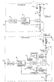
- the circuit shown in Figure 1 comprises a tamper-resistant enclosure 1.
- the enclosure may comprise a steel box having a steel lid welded thereto so as to prevent or render difficult unauthorised access to the circuit within the enclosure 1.
- the circuit further comprises an actuator 3, for instance of electromagnetic type forming part of an engine control system of a vehicle, having a recirculating diode 15 connected thereacross.
- the actuator may be part of the fuel system of a compression-ignition engine such that the engine cannot be operated unless the actuator 3 is enabled.
- the actuator is connected between a power supply terminal 4 in the form of a connector for supplying power to the circuit and, via a diode 5 for providing reverse supply polarity protection, to the drain of a power MOSFET 6, whose source is connected via a current sensing resistor 7 of very low value to a common terminal 2.
- the MOSFET 6 has a gate connected to the output of a pulse width modulator 8 having a control input connected to the connection between the current sensing resistor 7 and the source of the MOSFET 6.
- An enable input of the pulse width modulator 8 is connected to the output of a decoder 9, whose input is connected to an input terminal 10 of the circuit in the form of a connector.
- the common terminal 2 is electrically connected to the common terminal of a vehicle supply system.
- the power supply terminal 4 is connected to the vehicle power supply, for instance via the vehicle ignition switch.
- the input terminal 10 is connected to a controller which controls operation of the engine.
- the control system In order for the engine to be capable of operation, the control system must be capable of controlling operation of the actuator 3 by controlling conduction of the MOSFET 6.
- encoded signals are supplied by the controller to the decoder 9 via the input terminal 10.
- the decoder 9 decodes the encoded signals and, if these are correctly encoded, actuates the pulse width modulator 8.
- the pulse width modulator 8 senses the current by monitoring the voltage across the current sensing resistor 7 and controls the pulse width of a pulse waveform supplied to the gate of the MOSFET 6 so as to control the current which flows through the source/drain path of the MOSFET 6, and hence via the diode 5 through the actuator 3.
- the circuit shown in Figure 1 provides a high degree of resistance to tampering, it is possible for the circuit to be overridden by applying a relatively high voltage to the terminal 4 for a short duration. If a sufficiently large voltage is applied to the terminal 4 so that the maximum voltage rating of the source-drain path of the MOSFET 6 is exceeded, the MOSFET 6 will fail. In these circumstances, the source-drain path may fail open circuit or closed circuit and, if it fails closed circuit, the actuator 3 can then be operated without the thief needing to know the correct encoding for signals to the input terminal 10.
- a relatively low impedance actuator 3 may be used without requiring a MOSFET 6 of relatively high power rating. Additionally a low impedance actuator allows a high force to be generated for a short time. This force may be used to overcome any pressure in the system caused, for instance, during cranking.
- a fusible link 11 such as a conventional fuse, is connected between the diode 5 and the drain of the MOSFET 6.
- the gate of the MOSFET 6 is connected to the output of an OR gate 12 having first, second, and third inputs.
- the first input is connected to the output of the modulator 8
- the second input is connected to the output of a latch 16 whose input is connected to the output of a comparator 13
- the third input is connected to the output of a latch 17 whose input is connected to the output of a comparator 14.
- the comparator 13 has a non-inverting input connected via a filter 18 to the connection between the resistor 7 and the source of the MOSFET 6. An inverting input of the comparator 13 is connected to receive a first reference voltage Vr1.
- the comparator 14 has a non-inverting input connected via a filter 19 to the connection between the fusible link 11 and the drain of the MOSFET 6. An inverting input of the comparator 14 is connected to receive a second reference voltage Vr2.
- the filters 18 and 19 reduce noise and particularly transient voltages which may occur as interference from electrical systems of the vehicle and which might otherwise cause false triggering.
- the circuit of Figure 2 operates in the same way as the circuit of Figure 1 and permits the actuator 3 to be actuated only when the correctly encoded signal is supplied to the input 10.
- the fusible link 11 has a rating such that it passes the normal working current of the actuator 3 but goes open circuit at a predetermined current between the normal operating current of the actuator, as defined by the current drive provided by the pulse width modulator 8, and the current drawn by the actuator 3 with the MOSFET 6 short-circuited.
- the comparator 13 monitors the current passing through the actuator 3 by monitoring the voltage developed across the current sensing resistor 7. If the current exceeds a predetermined value defined by the first reference voltage Vr1, the comparator 13 actuates the latch 16 which turns on the MOSFET 6 via the gate 12 so that the fusible link 11 goes open circuit. Similarly, the comparator 14 monitors the voltage at the drain of the MOSFET 6. If this exceeds the second reference voltage Vr2, the comparator 14 actuates the latch 17 which switches on the MOSFET 6 via the gate 12. Again, this causes the actuator 3 and fusible link 11 to be connected across the power supply so that the fusible link 11 goes open circuit and the actuator 3 cannot be actuated. The latches 16 and 17 ensure that the MOSFET 6 is turned on for long enough to ensure that the fusible link 11 goes open circuit.
- the actuator 3 and/or the diode 5 and/or the fusible link 11 may be connected in the source circuit of the MOSFET 6 instead of in the drain circuit as shown.
- the current sensing resistor 7 may be connected in the drain circuit instead of in the source circuit.
- the MOSFET 6 may be replaced by any other suitable device, such as a bipolar transistor of appropriate rating.
- the enclosure 1 may actually form part of the actuator 3 with the remaining components being provided therein.
- the fusible link 11 may comprise a thermally actuated device which goes open circuit in response to a rise in temperature corresponding to currents greater than or equal to the predetermined current.
- the device may be automatically or manually resettable after a delay.
- circuit blocks 8, 9, 12, 13, 14, and 16 to 19 are shown as discrete blocks in Figure 2, any or all of them may be embodied within a single device, such as a micro-controller, for instance in the form of a VLSI integrated circuit with associated passive components.
Applications Claiming Priority (2)
| Application Number | Priority Date | Filing Date | Title |
|---|---|---|---|
| GBGB9512883.1A GB9512883D0 (en) | 1995-06-23 | 1995-06-23 | Tamper-resistant circuit |
| GB9512883 | 1995-06-23 |
Publications (2)
| Publication Number | Publication Date |
|---|---|
| EP0750112A2 true EP0750112A2 (de) | 1996-12-27 |
| EP0750112A3 EP0750112A3 (de) | 1998-01-28 |
Family
ID=10776604
Family Applications (1)
| Application Number | Title | Priority Date | Filing Date |
|---|---|---|---|
| EP96304410A Withdrawn EP0750112A3 (de) | 1995-06-23 | 1996-06-13 | Gegen äussere Eingriffe gesicherte Schaltung und Maschinensteuerungssystem |
Country Status (2)
| Country | Link |
|---|---|
| EP (1) | EP0750112A3 (de) |
| GB (1) | GB9512883D0 (de) |
Cited By (4)
| Publication number | Priority date | Publication date | Assignee | Title |
|---|---|---|---|---|
| WO1999014856A2 (de) * | 1997-09-16 | 1999-03-25 | Siemens Aktiengesellschaft | Verfahren und vorrichtung zum ansteuern einer integrierten leistungsendstufe |
| EP1050966A2 (de) * | 1999-03-17 | 2000-11-08 | Philips Corporate Intellectual Property GmbH | Schaltungsanordnung zum Steuern eines Aktuators |
| US6194951B1 (en) | 1998-09-15 | 2001-02-27 | Siemens Aktiengesellschaft | Method and device for diving an integrated power output stage |
| DE10121993A1 (de) * | 2001-05-05 | 2002-11-14 | Daimler Chrysler Ag | Zündsystem für Verbrennungsmotoren |
Citations (9)
| Publication number | Priority date | Publication date | Assignee | Title |
|---|---|---|---|---|
| GB2079837A (en) * | 1980-07-14 | 1982-01-27 | Royster John Lee | Security locking system |
| US4890185A (en) * | 1987-12-23 | 1989-12-26 | Lenze Gmbh & Co. Kg Aerzen | Circuit for protecting a switching transistor |
| FR2648631A1 (fr) * | 1989-06-16 | 1990-12-21 | Rexroth Sigma | Procede et montage pour proteger un circuit electrique pour au moins deux seuils distincts de courant |
| US5191228A (en) * | 1990-06-22 | 1993-03-02 | Sloan Jeffrey M | Vehicle battery disconnect antitheft device |
| FR2685267A1 (fr) * | 1991-12-24 | 1993-06-25 | Le Bail Hubert | Systeme anti-vol a commande par fibre optique (pour voitures automobiles). |
| EP0600751A2 (de) * | 1992-12-04 | 1994-06-08 | Texas Instruments Incorporated | Halbleiterleistungsregler |
| FR2710390A1 (fr) * | 1993-09-20 | 1995-03-31 | Sellem Albert | Dispositif de coupure d'un flux de fluide. |
| EP0660519A2 (de) * | 1993-12-23 | 1995-06-28 | Lucas Industries Public Limited Company | Halbleitervorrichtungsschutzschaltung |
| DE4414505A1 (de) * | 1994-04-26 | 1995-11-02 | Helmut Werner | Elektronische Wegfahrsperre für Kraftfahrzeuge |
-
1995
- 1995-06-23 GB GBGB9512883.1A patent/GB9512883D0/en active Pending
-
1996
- 1996-06-13 EP EP96304410A patent/EP0750112A3/de not_active Withdrawn
Patent Citations (9)
| Publication number | Priority date | Publication date | Assignee | Title |
|---|---|---|---|---|
| GB2079837A (en) * | 1980-07-14 | 1982-01-27 | Royster John Lee | Security locking system |
| US4890185A (en) * | 1987-12-23 | 1989-12-26 | Lenze Gmbh & Co. Kg Aerzen | Circuit for protecting a switching transistor |
| FR2648631A1 (fr) * | 1989-06-16 | 1990-12-21 | Rexroth Sigma | Procede et montage pour proteger un circuit electrique pour au moins deux seuils distincts de courant |
| US5191228A (en) * | 1990-06-22 | 1993-03-02 | Sloan Jeffrey M | Vehicle battery disconnect antitheft device |
| FR2685267A1 (fr) * | 1991-12-24 | 1993-06-25 | Le Bail Hubert | Systeme anti-vol a commande par fibre optique (pour voitures automobiles). |
| EP0600751A2 (de) * | 1992-12-04 | 1994-06-08 | Texas Instruments Incorporated | Halbleiterleistungsregler |
| FR2710390A1 (fr) * | 1993-09-20 | 1995-03-31 | Sellem Albert | Dispositif de coupure d'un flux de fluide. |
| EP0660519A2 (de) * | 1993-12-23 | 1995-06-28 | Lucas Industries Public Limited Company | Halbleitervorrichtungsschutzschaltung |
| DE4414505A1 (de) * | 1994-04-26 | 1995-11-02 | Helmut Werner | Elektronische Wegfahrsperre für Kraftfahrzeuge |
Cited By (8)
| Publication number | Priority date | Publication date | Assignee | Title |
|---|---|---|---|---|
| WO1999014856A2 (de) * | 1997-09-16 | 1999-03-25 | Siemens Aktiengesellschaft | Verfahren und vorrichtung zum ansteuern einer integrierten leistungsendstufe |
| WO1999014856A3 (de) * | 1997-09-16 | 1999-05-06 | Siemens Ag | Verfahren und vorrichtung zum ansteuern einer integrierten leistungsendstufe |
| US6194951B1 (en) | 1998-09-15 | 2001-02-27 | Siemens Aktiengesellschaft | Method and device for diving an integrated power output stage |
| EP1050966A2 (de) * | 1999-03-17 | 2000-11-08 | Philips Corporate Intellectual Property GmbH | Schaltungsanordnung zum Steuern eines Aktuators |
| EP1050966A3 (de) * | 1999-03-17 | 2002-01-30 | Philips Corporate Intellectual Property GmbH | Schaltungsanordnung zum Steuern eines Aktuators |
| DE10121993A1 (de) * | 2001-05-05 | 2002-11-14 | Daimler Chrysler Ag | Zündsystem für Verbrennungsmotoren |
| DE10121993B4 (de) * | 2001-05-05 | 2004-08-05 | Daimlerchrysler Ag | Zündsystem für Verbrennungsmotoren |
| US6823841B2 (en) | 2001-05-05 | 2004-11-30 | Daimlerchrysler Ag | Ignition system for internal combustion engines |
Also Published As
| Publication number | Publication date |
|---|---|
| EP0750112A3 (de) | 1998-01-28 |
| GB9512883D0 (en) | 1995-08-23 |
Similar Documents
| Publication | Publication Date | Title |
|---|---|---|
| US5895989A (en) | Power supply unit and connector connection failure detection method | |
| US6154081A (en) | Load circuit having extended reverse voltage protection | |
| US7345383B2 (en) | Abnormality detection apparatus for a power feed circuit | |
| JP3040342B2 (ja) | 電力用mosゲート型回路のための制御回路 | |
| KR101195439B1 (ko) | 전기 스티어링 잠금 장치 | |
| KR100347681B1 (ko) | 차량에있어서의부하의조작장치 | |
| KR20070049561A (ko) | 부하구동장치 | |
| US20080247108A1 (en) | Load drive device | |
| US5119312A (en) | Circuitry for surveillance of switching state of a power transistor | |
| KR20060046198A (ko) | 직류 전자장치용 릴레이 제어장치 | |
| EP0750112A2 (de) | Gegen äussere Eingriffe gesicherte Schaltung und Maschinensteuerungssystem | |
| US11955882B2 (en) | Safe active discharge circuit for inverter in vehicle | |
| KR20060109974A (ko) | 유도성 부하를 제어하기 위한 회로 장치 및 방법 | |
| JPH05130730A (ja) | Dc−dcコンバータの保護回路 | |
| JPH02297818A (ja) | 接点の電流制御装置 | |
| JP2000032650A (ja) | 負荷の制御のための方法及び装置 | |
| JP2000058756A (ja) | 双方向電子スイッチ | |
| KR100559248B1 (ko) | 차량 이씨유의 전원 입력회로 | |
| EP0660519B1 (de) | Halbleitervorrichtungsschutzschaltung | |
| JP3171383B2 (ja) | 保護回路 | |
| JPH0234471Y2 (de) | ||
| KR870001728B1 (ko) | 마이크로 프로세서의 런 어웨이(Run away) 방지방법 및 장치 | |
| KR100760854B1 (ko) | 모터 보호 회로 | |
| EP1373800B1 (de) | Steuer- und sicherheitsvorrichtung für ventile | |
| JPH0713534B2 (ja) | 安全弁の駆動回路 |
Legal Events
| Date | Code | Title | Description |
|---|---|---|---|
| PUAI | Public reference made under article 153(3) epc to a published international application that has entered the european phase |
Free format text: ORIGINAL CODE: 0009012 |
|
| AK | Designated contracting states |
Kind code of ref document: A2 Designated state(s): DE ES FR GB IT SE |
|
| PUAL | Search report despatched |
Free format text: ORIGINAL CODE: 0009013 |
|
| AK | Designated contracting states |
Kind code of ref document: A3 Designated state(s): DE ES FR GB IT SE |
|
| 17P | Request for examination filed |
Effective date: 19980728 |
|
| 17Q | First examination report despatched |
Effective date: 19991025 |
|
| RAP1 | Party data changed (applicant data changed or rights of an application transferred) |
Owner name: LUCAS INDUSTRIES LIMITED |
|
| RAP1 | Party data changed (applicant data changed or rights of an application transferred) |
Owner name: LUCAS INDUSTRIES LIMITED |
|
| STAA | Information on the status of an ep patent application or granted ep patent |
Free format text: STATUS: THE APPLICATION IS DEEMED TO BE WITHDRAWN |
|
| 18D | Application deemed to be withdrawn |
Effective date: 20030108 |