EP0739146A2 - Fernmeldevermittlungssystem - Google Patents
Fernmeldevermittlungssystem Download PDFInfo
- Publication number
- EP0739146A2 EP0739146A2 EP96302294A EP96302294A EP0739146A2 EP 0739146 A2 EP0739146 A2 EP 0739146A2 EP 96302294 A EP96302294 A EP 96302294A EP 96302294 A EP96302294 A EP 96302294A EP 0739146 A2 EP0739146 A2 EP 0739146A2
- Authority
- EP
- European Patent Office
- Prior art keywords
- switch
- nodes
- array
- peripherals
- node
- Prior art date
- Legal status (The legal status is an assumption and is not a legal conclusion. Google has not performed a legal analysis and makes no representation as to the accuracy of the status listed.)
- Withdrawn
Links
Images


Classifications
-
- H—ELECTRICITY
- H04—ELECTRIC COMMUNICATION TECHNIQUE
- H04Q—SELECTING
- H04Q3/00—Selecting arrangements
- H04Q3/64—Distributing or queueing
- H04Q3/68—Grouping or interlacing selector groups or stages
Definitions
- This invention relates to large capacity telecommunications switches constructed using a matrix (modular) architecture, and is particularly concerned with the provision of redundancy to provide a measure of protection against failure of the switch caused by failure of an individual component thereof.
- n smaller capacity switches, node switches, 10.1, 10.2 ...10.n which are employed as buffers/time switches, on the periphery are connected to each other via an optical space switch core 1 1 which is functionally an n ⁇ n crosspoint.
- This core 11 may be implemented as a broadcast and select network arranged such that the incoming data streams from each of the n node switches 10 is first split n, ways and then a selector mechanism (not shown) chooses which parts of the incoming data streams shall be onwardly directed to which node switch.
- the selector mechanism forms part of the core 11, and therefore, from the outside, the core appears as a crosspoint.
- the connections in the core 11 are re-arranged according to the traffic presented using a grant/request mechanism (not shown) under the control of core scheduler (not shown).
- FIG. 1 The arrangement of Figure 1 can be re-drawn, as depicted in Figure 2, to resemble a series of switches interconnected via a n-line bus 20.
- Each node switch 10.1, 10.2 .... 10.n transmits on an associated line 20.1, 20.2.... 20.n of the bus, but can receive from any line.
- a selector 21.1, 21.2 ....21.n associated with each node switch determines which line is to be received by that node-switch at any given time.
- the switch of Figure 2 is completely equivalent to that of Figure 1, but suggests a different partitioning in which the selection of the required signal is performed at the node switch rather than in the core, which latter thus becomes a completely passive arrangement of optical waveguide splitters and connectors.
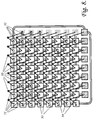
- n ⁇ m matrix arrangement of buffers and buses can be employed to make a large switch from an assembly of smaller units (nodes).
- n ⁇ n nodes 30 are arranged in a square matrix.
- Each node 30 has an external input port 31, an external output port 32, and internal input and output ports connected to vertical and horizontal buses 33 and 34.
- a signal applied to the external input 31 port of any particular node 30 can be routed by the switch to the external output port of any other node by propagation along the buses 33 and 34 and through, in most instances, a sequence of three modes.
- a signal applied to the external input port of node A and destined for the external output port of node D can follow the route ABD or the route ACD. More complicated routes e.g. AEFD are also possible if, for instance, required because of failure of some component.
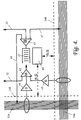
- An individual node 30 of the switch of Figure 3 may take the form illustrated in Figure 4. This depicts the external input and output ports 31 and 32, and the vertical and horizontal buses 33 and 34 which convey data over lines 37a and 34a, and control signals over lines 33b and 34b, with request and grant control signals R, G to and from a traffic control 40.
- a buffer 41 process inputs from a multiplexer 42 and provides outputs to a demultiplexer 43.
- the multiplexer 42 has three inputs comprising the external input 31, an input from the vertical data bus 33a via a bus line selector 44, and an input from the horizontal data bus 34a via bus line selector 45.
- the demultiplexer similarly has three outputs comprising the external output 32 and inputs 46 and 47 respectively to the vertical and horizontal data buses 33a and 34a.
- the input and output ports 31 and 32 of each of the n ⁇ n nodes will be connected to a peripheral (not shown) associated with that node. It is normal practice to provide dual fabrics for fault protection, which would imply that the n ⁇ n associated peripherals would be connected not only to the switch fabric of Figure 3 in one plane, but also to duplicate of that switch fabric in an adjacent plane. The peripherals would normally also be duplicated or for instance each of a set of line cards connected to the switch would be connected to two different peripherals. Now in these circumstances, if the switch were a 16 x 16 matrix, then there will be 256 nodes in one plane, and a further 256 nodes in the other plane.
- the first plane matrix will be active while the second plane matrix remains redundant (inactive) until a fault occurs in the first plane matrix, and at this stage the second plane matrix is activated. It is most likely that no more than one node or one bus will fail at any one time, and so for the sake of a single node failure that leaves 255 still in working order, all these 255 nodes are disabled by the activation of the second plane matrix and the consequently closing down of the first plane matrix.
- the present invention is directed to obtaining efficient redundancy with reduced hardware duplication.
- a telecommunications switch having a matrix architecture of bus-interconnected switch nodes and having switch peripherals connected to each of the switch nodes externally of the bus-interconnected matrix, characterised in that redundancy of operation is afforded by providing each one of said peripherals with enable/disable connections to two different switch nodes of the matrix.
- the invention also provides a telecommunications switch having a matrix architecture of space-switch interconnected switch nodes and having switch peripherals connected to each of the switch nodes externally of the space-switch interconnected matrix, characterised in that redundancy of operation is afforded by providing each one of said peripherals with enable/disable connections to two different switch nodes of the matrix.
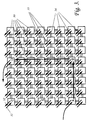
- a telecommunications switch having a matrix architecture bus-interconnected switch nodes 30 in an n ⁇ n array.
- switch nodes 30 Additional to the n ⁇ n array of nodes are 2n-1 further switch nodes 30, distinguished in Figures 5 and 6 by a diagonal hatching, and arranged in a row and a column to the right of and below the n ⁇ n main array.
- Each switch node 30 has a pair of internal ports respectively connected to the vertical and horizontal buses 33 and 34.
- each of these nodes will be labelled with a pair of numbers indicating the row and column position of that node in the array, numbering from the top right-hand corner.
- switch node 30(1, 1) is the top right-hand corner switch node
- switch node 30(p, q) is the node that is at the intersection of row p with column q.
- Each switch node 30 has a pair of internal ports respectively connected to vertical and horizontal buses 33 and 34.
- switch node 30(p,q) has its internal parts respectively connected to horizontal bus 34(p) and to vertical bus 33(q).
- Each switch node 30 also has a pair of external ports for connection to individual members of an n ⁇ n notional array of peripherals 50 which are labelled in the same way as the switch nodes 30.
- the assembly of switch nodes 30 have been described as constituting an array because of the two dimensional bus connections between its members, but this is not to be understood as necessarily implying that they are actually arranged in a physical array of rows and columns.
- peripherals 50 have been described as constituting a 'notional' array because the absence of direct interconnections between its members makes the due array-like characteristics of this assembly even more tenuous.)
- the first external ports of the additional switch nodes (shown with diagonal hatching) of row n+1 and column n+1 are left unconnected, while the first external parts of all the other switch nodes are connected by connections 51 to their corresponding peripherals having the same row and column numbers.
- the first external port of switch node 30(p,q) is connected by a connection 51 to peripheral 50(p,q).
- the second external ports of the switch nodes of row 1 and column 1 are similarly left unconnected, while those of all the other switch nodes are connected by connections 52 to the peripherals with the next lower row and column numbers.
- the second external port of switch node 30(p,q) is connected by a connection 52 to peripheral 50(p-1, q-1). Prior to any failure of the switch all the connections 51 are enabled, while all the connections 52 are disabled.
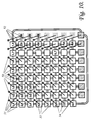
- FIG. 7 Such a switch is depicted in Figure 7.
- this switch there is an array of n ⁇ n switch nodes 30, plus the additional 2n-1 switch nodes, each of which is provided with a pair of external ports 70, 71 connected to an n ⁇ n array of peripherals 50 by connections 51 and 52 arranged in the same manner as in the switch of Figure 5.
- Each switch node 30 additionally has a pair of internal ports 72 and 73.
- each switch node 30 is connected to a member of a set of n+1 space switch (n+1) ⁇ (n+1) cores 74 according to the row number of that switch node in the array.
- its internal port 73 is connected to a member of a set of n+1 space switch (n+1) ⁇ (n+1) cores 75 according to the column number of the switch node in the array.
- connection 52 shown to link peripheral 50(p,n) with phantom switch node 30(p+1, n+1) is, for all values of p in the range 1 ⁇ p ⁇ n-1, actually a connection 51 linking peripheral 50(p,n) with real switch node 30(n+1, p+1).
- the horizontal bus connection to the phantom switch node 30(p+1, n+1) is actually the horizontal bus connection to real switch node 30(n+1, p+1).
- the horizontal and vertical bus connections to switch node 30(n+1, n+1) are respectively to the horizontal bus 34 of row 1 and to the vertical bus 33 of column 1.
- a connection, routed before failure, from peripheral 50(6,1) to peripheral 50(8,7) by way of switch nodes 30(6,1), 30(6,7) and 30(8,7), can be routed (Figure 9), after failure, via one of the additional switch nodes of row 9, for instance by way of switch nodes 30(6,1), 30(9,9), 30(1,7) and 30(8,7), or 30(6,1), 30(9,6), 30(8,1) and 30(8,7).
- this can be overcome by making use of the inherent routing diversity in the network to redistribute the displaced traffic more effectively, and/or by connecting the unused external ports of the switch nodes 30 of row 1 and column 1 of the switch node matrix in a manner providing additional bus capacity.
- the particular matrix array of switch nodes of the switch of Figures 8, 9 and 10, excluding the additional switch nodes of row n+1, is a square n ⁇ n array
- the basic arrangement is applicable, with minor modification, also to rectangular n ⁇ m arrays in which n ⁇ m. Since the rows and columns are essentially interchangeable, attention may be confined without loss of generality to the situation in which n ⁇ m.
- the n phantom switch nodes 30(p, n+1), where 2 ⁇ p ⁇ n are mapped on to the n real switch nodes 30(n+1,q), where 2 ⁇ q ⁇ n.
- the rectangular array situation is distinguished from the square array one by the presence of a choice in the mapping. It will generally be preferred for this choice to be exercised in a way that avoids mapping any of the phantom nodes on to additional switch node 30(n+1, m) since this avoids the situation of having a peripheral 50 with connections 51 and 52 to switch nodes sharing a common vertical bus 33.
- An example of a mapping which avoids this is the one in which phantom switch node 30(p, m+1), where 2 ⁇ p ⁇ n, maps on to real switch node 30(n+1, p).
- the switch node matrices of the switches of Figures 5 to 10 have all been provided with additional switch nodes 30 for the purposes of redundancy for fault protection. It has been shown that this use of additional switch nodes leaves some switch nodes in the matrix with unused ports.
- these switch nodes with unused ports are to be found in the top row and the left-hand column of the switch node matrix, but with alternative interconnection schemes they can be located elsewhere in the matrix.
- the presence of the unused ports indicates that some or all of the additional switch nodes 30 can be dispensed with, while retaining the requisite redundancy for instance by additional bus connections utilising the previously unused ports.
Landscapes
- Engineering & Computer Science (AREA)
- Computer Networks & Wireless Communication (AREA)
- Use Of Switch Circuits For Exchanges And Methods Of Control Of Multiplex Exchanges (AREA)
- Data Exchanges In Wide-Area Networks (AREA)
- Monitoring And Testing Of Exchanges (AREA)
Applications Claiming Priority (2)
| Application Number | Priority Date | Filing Date | Title |
|---|---|---|---|
| GB9507980 | 1995-04-19 | ||
| GB9507980A GB2300088B (en) | 1995-04-19 | 1995-04-19 | Telecommunications switches |
Publications (2)
| Publication Number | Publication Date |
|---|---|
| EP0739146A2 true EP0739146A2 (de) | 1996-10-23 |
| EP0739146A3 EP0739146A3 (de) | 2000-03-29 |
Family
ID=10773215
Family Applications (1)
| Application Number | Title | Priority Date | Filing Date |
|---|---|---|---|
| EP96302294A Withdrawn EP0739146A3 (de) | 1995-04-19 | 1996-04-01 | Fernmeldevermittlungssystem |
Country Status (4)
| Country | Link |
|---|---|
| US (1) | US5986572A (de) |
| EP (1) | EP0739146A3 (de) |
| JP (1) | JPH08331615A (de) |
| GB (1) | GB2300088B (de) |
Cited By (1)
| Publication number | Priority date | Publication date | Assignee | Title |
|---|---|---|---|---|
| EP1009173A1 (de) * | 1998-12-07 | 2000-06-14 | Alcatel | Fehlertolerantes Koppelfeld mit binären Schaltelementen |
Families Citing this family (4)
| Publication number | Priority date | Publication date | Assignee | Title |
|---|---|---|---|---|
| US5923643A (en) * | 1997-02-27 | 1999-07-13 | Excel, Inc. | Redundancy, expanded switching capacity and fault isolation arrangements for expandable telecommunications system |
| JP2009060225A (ja) * | 2007-08-30 | 2009-03-19 | Fujitsu Ltd | Rf回線切り替え回路 |
| US8930872B2 (en) * | 2012-02-17 | 2015-01-06 | Netronome Systems, Incorporated | Staggered island structure in an island-based network flow processor |
| US8902902B2 (en) | 2012-07-18 | 2014-12-02 | Netronome Systems, Incorporated | Recursive lookup with a hardware trie structure that has no sequential logic elements |
Family Cites Families (4)
| Publication number | Priority date | Publication date | Assignee | Title |
|---|---|---|---|---|
| US4630258A (en) * | 1984-10-18 | 1986-12-16 | Hughes Aircraft Company | Packet switched multiport memory NXM switch node and processing method |
| US5123011A (en) * | 1989-09-27 | 1992-06-16 | General Electric Company | Modular multistage switch for a parallel computing system |
| US5303078A (en) * | 1990-12-18 | 1994-04-12 | Bell Communications Research, Inc. | Apparatus and method for large scale ATM switching |
| JP2770936B2 (ja) * | 1990-12-18 | 1998-07-02 | インターナショナル・ビジネス・マシーンズ・コーポレイション | 通信ネットワークおよび通信チャンネルをつくる方法 |
-
1995
- 1995-04-19 GB GB9507980A patent/GB2300088B/en not_active Expired - Fee Related
-
1996
- 1996-04-01 EP EP96302294A patent/EP0739146A3/de not_active Withdrawn
- 1996-04-18 JP JP8096847A patent/JPH08331615A/ja not_active Withdrawn
- 1996-04-19 US US08/634,912 patent/US5986572A/en not_active Expired - Fee Related
Cited By (3)
| Publication number | Priority date | Publication date | Assignee | Title |
|---|---|---|---|---|
| EP1009173A1 (de) * | 1998-12-07 | 2000-06-14 | Alcatel | Fehlertolerantes Koppelfeld mit binären Schaltelementen |
| FR2790631A1 (fr) * | 1998-12-07 | 2000-09-08 | Cit Alcatel | Matrice de commutateurs a deux positions chacun |
| US6373151B1 (en) | 1998-12-07 | 2002-04-16 | Alcatel | Matrix of two-position switches |
Also Published As
| Publication number | Publication date |
|---|---|
| EP0739146A3 (de) | 2000-03-29 |
| GB2300088A (en) | 1996-10-23 |
| GB9507980D0 (en) | 1995-06-07 |
| US5986572A (en) | 1999-11-16 |
| GB2300088B (en) | 1999-06-16 |
| JPH08331615A (ja) | 1996-12-13 |
Similar Documents
| Publication | Publication Date | Title |
|---|---|---|
| JP2666533B2 (ja) | スイツチモジユール | |
| CA1225729A (en) | Fault-tolerant array of cross-point switching matrices | |
| US9584373B2 (en) | Configurable Clos network | |
| US6567576B2 (en) | Optical switch matrix with failure protection | |
| US4983961A (en) | Three stage non-blocking switching array | |
| JPH03154544A (ja) | 分散制御型クロスポイント交換機 | |
| JPH06501831A (ja) | 非線形転送モードスイッチング構成 | |
| US5198808A (en) | Matrix switch apparatus with a diagnosis circuit having stand-by ports and reduced size matrix switching elements | |
| JPS6244760B2 (de) | ||
| US4903259A (en) | Time-division multiplex switching network | |
| US5986572A (en) | Telecommunications switches | |
| AU628503B2 (en) | Improvements in or relating to exchanges | |
| US7170895B2 (en) | Switch and a switching apparatus for a communication network | |
| US4398285A (en) | Time-division multiplex switching network | |
| US5142686A (en) | Multiprocessor system having processors and switches with each pair of processors connected through a single switch using Latin square matrix | |
| JPH0834610B2 (ja) | 多段スイッチ装置 | |
| JP3795082B2 (ja) | 通信システムに関する構成並びに方法 | |
| JP2977344B2 (ja) | 光ファイバ伝送システム | |
| SU877548A1 (ru) | Устройство дл управлени переключением резерва | |
| US6373151B1 (en) | Matrix of two-position switches | |
| GB1181181A (en) | Switching Network | |
| JPH0714225B2 (ja) | 交換スイツチ | |
| GB1588150A (en) | Switching networks for use in telecommunications system | |
| JPH0744710B2 (ja) | 空間分割スイツチネツトワーク | |
| JPH04158693A (ja) | 5段スイッチの診断方式 |
Legal Events
| Date | Code | Title | Description |
|---|---|---|---|
| PUAI | Public reference made under article 153(3) epc to a published international application that has entered the european phase |
Free format text: ORIGINAL CODE: 0009012 |
|
| AK | Designated contracting states |
Kind code of ref document: A2 Designated state(s): DE FR SE |
|
| RAP3 | Party data changed (applicant data changed or rights of an application transferred) |
Owner name: NORTEL NETWORKS CORPORATION |
|
| PUAL | Search report despatched |
Free format text: ORIGINAL CODE: 0009013 |
|
| AK | Designated contracting states |
Kind code of ref document: A3 Designated state(s): DE FR SE |
|
| RIC1 | Information provided on ipc code assigned before grant |
Free format text: 7H 04Q 3/68 A, 7H 04Q 11/00 B |
|
| RAP1 | Party data changed (applicant data changed or rights of an application transferred) |
Owner name: NORTEL NETWORKS LIMITED |
|
| 17P | Request for examination filed |
Effective date: 20000929 |
|
| RAP1 | Party data changed (applicant data changed or rights of an application transferred) |
Owner name: NORTEL NETWORKS LIMITED |
|
| STAA | Information on the status of an ep patent application or granted ep patent |
Free format text: STATUS: THE APPLICATION HAS BEEN WITHDRAWN |
|
| 18W | Application withdrawn |
Effective date: 20050311 |