EP0731545A2 - Circuit et méthode pour la commande de charge d'une batterie - Google Patents
Circuit et méthode pour la commande de charge d'une batterie Download PDFInfo
- Publication number
- EP0731545A2 EP0731545A2 EP96103050A EP96103050A EP0731545A2 EP 0731545 A2 EP0731545 A2 EP 0731545A2 EP 96103050 A EP96103050 A EP 96103050A EP 96103050 A EP96103050 A EP 96103050A EP 0731545 A2 EP0731545 A2 EP 0731545A2
- Authority
- EP
- European Patent Office
- Prior art keywords
- battery
- coupled
- voltage
- transistor
- output
- Prior art date
- Legal status (The legal status is an assumption and is not a legal conclusion. Google has not performed a legal analysis and makes no representation as to the accuracy of the status listed.)
- Withdrawn
Links
Images


Classifications
-
- H—ELECTRICITY
- H02—GENERATION; CONVERSION OR DISTRIBUTION OF ELECTRIC POWER
- H02J—CIRCUIT ARRANGEMENTS OR SYSTEMS FOR SUPPLYING OR DISTRIBUTING ELECTRIC POWER; SYSTEMS FOR STORING ELECTRIC ENERGY
- H02J7/00—Circuit arrangements for charging or depolarising batteries or for supplying loads from batteries
- H02J7/0013—Circuit arrangements for charging or depolarising batteries or for supplying loads from batteries acting upon several batteries simultaneously or sequentially
- H02J7/0014—Circuits for equalisation of charge between batteries
- H02J7/0016—Circuits for equalisation of charge between batteries using shunting, discharge or bypass circuits
-
- H—ELECTRICITY
- H02—GENERATION; CONVERSION OR DISTRIBUTION OF ELECTRIC POWER
- H02J—CIRCUIT ARRANGEMENTS OR SYSTEMS FOR SUPPLYING OR DISTRIBUTING ELECTRIC POWER; SYSTEMS FOR STORING ELECTRIC ENERGY
- H02J7/00—Circuit arrangements for charging or depolarising batteries or for supplying loads from batteries
- H02J7/0013—Circuit arrangements for charging or depolarising batteries or for supplying loads from batteries acting upon several batteries simultaneously or sequentially
- H02J7/0014—Circuits for equalisation of charge between batteries
- H02J7/0019—Circuits for equalisation of charge between batteries using switched or multiplexed charge circuits
-
- H—ELECTRICITY
- H02—GENERATION; CONVERSION OR DISTRIBUTION OF ELECTRIC POWER
- H02J—CIRCUIT ARRANGEMENTS OR SYSTEMS FOR SUPPLYING OR DISTRIBUTING ELECTRIC POWER; SYSTEMS FOR STORING ELECTRIC ENERGY
- H02J7/00—Circuit arrangements for charging or depolarising batteries or for supplying loads from batteries
- H02J7/0029—Circuit arrangements for charging or depolarising batteries or for supplying loads from batteries with safety or protection devices or circuits
- H02J7/00308—Overvoltage protection
-
- H—ELECTRICITY
- H02—GENERATION; CONVERSION OR DISTRIBUTION OF ELECTRIC POWER
- H02J—CIRCUIT ARRANGEMENTS OR SYSTEMS FOR SUPPLYING OR DISTRIBUTING ELECTRIC POWER; SYSTEMS FOR STORING ELECTRIC ENERGY
- H02J7/00—Circuit arrangements for charging or depolarising batteries or for supplying loads from batteries
- H02J7/0029—Circuit arrangements for charging or depolarising batteries or for supplying loads from batteries with safety or protection devices or circuits
- H02J7/0036—Circuit arrangements for charging or depolarising batteries or for supplying loads from batteries with safety or protection devices or circuits using connection detecting circuits
-
- H—ELECTRICITY
- H02—GENERATION; CONVERSION OR DISTRIBUTION OF ELECTRIC POWER
- H02J—CIRCUIT ARRANGEMENTS OR SYSTEMS FOR SUPPLYING OR DISTRIBUTING ELECTRIC POWER; SYSTEMS FOR STORING ELECTRIC ENERGY
- H02J7/00—Circuit arrangements for charging or depolarising batteries or for supplying loads from batteries
- H02J7/007—Regulation of charging or discharging current or voltage
- H02J7/00712—Regulation of charging or discharging current or voltage the cycle being controlled or terminated in response to electric parameters
- H02J7/007182—Regulation of charging or discharging current or voltage the cycle being controlled or terminated in response to electric parameters in response to battery voltage
Definitions
- the present invention relates in general to battery cell monitoring and charging and, more particularly, to battery cell charge balancing.
- Batteries are used in a wide variety of applications including digital pagers, cellular telephones, notebook computers, and in general, portable consumer electronics. Batteries employed in portable electronics include lithium ion, lithium polymer, nickel-cadmium, or nickel-metal hydride compositions. Since many of the applications require potentials of 12.0 volts or greater, multiple battery cells are often serially connected in a battery pack to provide the required operating potential. Once the batteries have been discharged by shelf life or during normal use in an application, it becomes necessary to recharge the battery pack. Problems of overcharging and undercharging of cells are encountered when battery packs are exposed to the recharging process. Overcharging of cells results in potentially dangerous and catastrophic failures in lithium based chemistries while over-discharged cells experience decreased cell life for all battery chemistries.
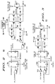
- battery charge control circuit 10 is shown suitable for manufacturing as a monolithic integrated circuit (IC) using conventional integrated circuit processes.
- Battery cells 12, 14, 16 and 18 are serially coupled between power supply conductor 20 (PACK+) and node 22 power supply conductor.
- Battery cells 12, 14, 16 and 18 are preferably lithium ion or polymer type rechargeable batteries, where the lithium ion cells operate at 4.2 volts and the polymer cells operate at 3.0 volts under a full charge.
- PROG1 and PROG2 inputs to control circuit 32 provide for a binary programming code representing the total number of battery cells presented to battery charge control circuit 10. A list of binary programming codes for up to four battery cells is shown in Table 1.
- the cells are replaced with a short circuit. For example, if three cells are programmed, battery cell 12 is replaced with a short circuit. Additional PROG inputs are incorporated to accommodate a battery system having more than four cells. Table 1 Number of cells PROG1 Input PROG2 Input 4 0 0 3 1 1 2 1 0 1 0 1
- Current sense resistor 11 and current sense resistor 15 are serially coupled between power supply conductor 20 and battery cell 12.
- Node 22 is coupled to the source of discharge transistor 24.
- the drain of transistor 24 is coupled to the drain of charge transistor 26.
- the source of transistor 26 is coupled to power supply conductor 30 (PACK-).
- Diode 25 has an anode coupled to the source of transistor 24 and a cathode coupled to the drain of transistor 24.
- Diode 25 is inherent in the structure of transistor 24.
- Diode 27 has an anode coupled to the source of transistor 26, and a cathode coupled to the drain of transistor 26.
- Diode 27 is inherent in the structure of transistor 24.
- Power supply conductors 20 and 30 represent the positive and negative terminals of the battery pack formed by battery cells 12-18.
- Transistor 24 receives a DISCHARGE (DISCH) signal at node 45 from the output of under-voltage logic (UV logic) circuit 62.
- the gate of transistor 26 is coupled to the output of OV logic circuit 60, at node 44, to receive a CHARGE (CHG) signal.
- An input of OV logic circuit 60 is coupled to receive the SET CHARGE (SET CHG) signal from an output of over-current logic (OI logic) circuit 37.
- Transistor 41 has a drain coupled to node 22, a gate coupled to an output of over-current logic circuit 37, and a source coupled to a terminal 43 for connection to an external resistor located within a battery charger. Transistor 41 could also be a bipolar transistor.
- OI logic circuit 37 receives a signal from the output of over-current detect circuit (OI detect) 35, the SLOW CLOCK signal from control circuit 32, and the OV signal from OV logic circuit 60.
- Transistor 41 of OI logic circuit 60 simulates the behavior of a thermistor.
- Nickel technology based battery chargers have a terminal that is used for a thermistor connection.
- transistor 41 is activated, causing the battery charger to operate in a trickle current charge mode.
- the thermistor simulation device disables the large value nickel technology charging currents that normally are applied to the battery pack. The lithium technology battery pack is therefore protected from dangerous overcharging.
- OI DETECT circuit 35 The inputs of OI DETECT circuit 35 are coupled across sense resistor 11.
- OI DETECT circuit 35 has a second output coupled to the SET input of UV logic 62 through delay circuit 61.
- the SET input of UV logic 62 is activated to disconnect the cells from the current path.
- Delay circuit 61 includes two flip-flops (not shown) coupled in series to provide the desired delay. Delay circuit 61 could also be made from a chain of gates coupled in series. Delay circuit 61 provides a 20.0 millisecond delay of the IO detect 35 output signal to compensate for connecting the battery pack to a capacitive load.
- the DISCHARGE and CHARGE signals at the gates of transistors 24 and 26, respectively, enable and disable the conduction path between power supply conductors 20 and 30. If the battery charge control circuit described hereinafter determines that an over-voltage condition or under-voltage condition exists on any individual battery cell, then transistor 24 and/or transistor 26 disables the conduction path between power supply conductors 20 and 30. Transistors 24 and 26 are placed as external components or are integrated into the IC containing battery charge control circuit 10.
- Cell measurement circuit 51 includes multiplexers 34 and 42, resistors 46, 48 and 50, switching circuit 56 and comparator 52.
- Analog multiplexer 34 has a first data input D1 coupled to power supply conductor 20 and a second data input D2 coupled to node 36 at the interconnection between battery cells 12 and 14.
- Multiplexer 34 further includes a third data input D3 coupled to node 38 at the interconnection between battery cells 14 and 16, and a fourth data input D4 coupled to node 40 at the interconnection of battery cells 16 and 18.
- Analog multiplexer 42 has four data inputs D1-D4 also coupled to nodes 36, 38, 40 and 22, respectively.
- Multiplexers 34 and 42 receive control signals SELECT1, SELECT0, and ENABLE (EN) from the outputs of control circuit 32, respectively.
- the output of multiplexer 34 is coupled to one side of serially coupled resistors 46, 48 and 50.
- the output of multiplexer 42 is coupled to the opposite side of the serially coupled resistors 46, 48 and 50.
- Comparator circuit 52 has a non-inverting input terminal coupled by way of switch 56 to either the interconnection of resistors 46 and 48 at node 54 or to the interconnection of resistors 48 and 50 at node 58.
- Control circuit 32 controls switch 56 with the SWITCH control signal.
- the inverting input terminal of comparator 52 receives a reference potential V REF operating at 1.25 volts.
- the STATUS signal output of comparator 52 is coupled to inputs of over-voltage logic 60, under-voltage logic 62, and to control circuit 32.
- the output of under-voltage logic 62 also provides an input to clock 32 for enabling a system clock signal output (SYSCLK) from clock circuit 64 that is coupled to an input of control circuit 32.
- Over-voltage logic 60 and under-voltage logic 62 receive signals OV_CLOCK and UV_CLOCK, respectively, from control circuit 32.
- Control circuit 32 also provides a hysteresis current (IHYST) coupled between the non-inverting input of comparator 52 and switch 56.
- IHYST hysteresis current
- Discharge transistors 212 and 214 are coupled across battery cells 12 and 14, respectively.
- the drain of transistor 212 is further coupled through resistor 220 to node 36
- the drain of transistor 214 is further coupled through resistor 222 to node 38.
- Discharge transistors 216 and 218 are coupled across battery cells 16 and 18, respectively.
- the drain of transistor 216 is coupled through resistor 224 to node 38
- the drain of transistor 218 is coupled through resistor 226 to node 40.
- the gates of transistors 212, 214, 216 and 218 receive battery control signals BAT1, BAT2, BAT3 and BAT4, respectively, from control circuit 32.
- Pack sense 240 circuit has a first input coupled to power supply conductor 30, a second input coupled to node 44, a first output providing a CHARGE DETECT (CHG DET) signal coupled to a reset of under-voltage logic 62, and a second output for providing a PACK STRETCH (PACK STR) signal to an input of over-current logic circuit 37.
- CHG DET CHARGE DETECT
- PACK STR PACK STRETCH
- battery charge control circuit 10 proceeds as follows. When the battery pack becomes discharged due to self-discharge of the battery cells or usage in a system, it is necessary to re-charge battery cells 12, 14, 16 and 18.
- An external power source e.g. battery charger, is coupled to power supply conductors 20 and 30 and a re-charge current is pumped into battery cells 12, 14, 16 and 18.
- a battery pack inserted in a battery charger contains individual battery cells exhibiting a mixed state of charge, i.e., one battery cell is in an acceptable charged state, another battery cell is in an overcharged state, while another battery cell is in an undercharged state, or any combination of the above.
- battery charge control circuit 10 balances the charge within the battery cells of the cell pack to enhance battery pack lifetime and safety.
- Battery charge control circuit 10 sequentially samples the voltage across each battery cell and identifies when the battery cells reach an unbalanced condition during charging. A battery cell is in balance with another battery cell if the first battery cell is within the hysteresis voltage VHYST of the other cells in the battery pack. Battery charge control circuit 10 uses the over-voltage limit set by comparator 52 and resistors 46, 48 and 50 as the criteria for balancing. If, in the case of charging the battery pack, one or more battery cells is sampled at an over-voltage by comparator 52, the measurement is transferred into control circuit 32. If all battery cells 12, 14, 16 and 18 in the battery pack are measured as over-voltage, the battery pack is considered balanced. If less than all cells are over-voltage at the same time, the over-voltage cells are discharged by battery charge control circuit 10 to bring the over-voltage cells in balance with the remainder of the battery cells.
- Control signals SELECT0 and SELECT1, controlling multiplexers, 34 and 42 cycle between selecting data inputs D1, D2, D3 and D4 of each multiplexer to sequentially sample battery cells 12, 14, 16 and 18.
- the control signals SELECT0 and SELECT1 select the D1 input of multiplexer 34 to pass the voltage at power supply conductor 20 to the top side of resistor 46.
- the control signals SELECT0 and SELECT1 enable the D1 input of multiplexer 42 to pass the voltage at node 36 to the bottom side of resistor 50.
- the voltage across battery cell 12 appears across serial resistors 46, 48 and 50.
- control circuit 32 further controls switch 56 to connect node 58 to the non-inverting input of comparator 52 to check for an over-voltage fault.
- the voltage at node 58 is a resistor divider ratio of the value of resistor 50 divided by the sum of resistors 46, 48 and 50.
- the value of resistors 46 is selected at 102.25 Kohms, and resistor 48 is set to 30.55 Kohms, while resistor 50 is set to 55.0 Kohms.
- the values chosen for the resistors can be adjusted for varying battery cell technologies. Resistors 46, 48, and 50 can also be selected to be placed external to the integrated circuit.
- V OV V REF x R50 R50 + R48 + R46
- control signals SELECT0 and SELECT1 select the D2 inputs of multiplexers 34 and 42 to pass the voltage at node 36 to the top side of resistor 46 and the voltage at node 38 to the bottom side of resistor 50.
- Comparator 52 performs an over-voltage check of battery cell 14 as described above. The process repeats to select the D3 inputs of multiplexers 34 and 42 to pass the voltage at node 38 to the top side of resistor 46 and the voltage at node 40 to the bottom side of resistor 50. Comparator 52 performs an over-voltage check of battery cell 16.
- control signals SELECT0 and SELECT1 finally select the D4 inputs of multiplexers 34 and 42 to pass the voltage at node 40 to the top side of resistor 46 and the voltage at node 22 to the bottom side of resistor 50.
- Comparator 52 performs an over-voltage check of battery cell 18. If fewer than four cells are programmed by the PROG1 and PROG2 inputs, the non-selected, shorted cells are not sampled by multiplexers 34 and 42.
- battery charge control circuit 10 detects an over-voltage, i.e. overcharge, condition in one battery cell, it initiates a discharge function for that battery cell immediately after comparing it to the condition of the other battery cells.
- the discharge function operates as follows. If the battery pack has been placed in a compatible charger, and if one battery cell is determined to be in an over-voltage condition, charge transistor 26 is "off” and discharge transistor 24 is "on”. Clock 64 continues to run and the battery balancing mode is enabled. If battery cell 12 is in the over-voltage condition while battery cells 14, 16 and 18 are not in an over-voltage condition, the STATUS input of control circuit 32 activates BAT4 control circuit output immediately after comparing it to the condition of the other battery cells. BAT4 signal turns "on" transistor 212, i.e. the discharge circuit, causing battery cell 12 to discharge at a rate limited by the "on” voltage combination of transistor 212 in series with the resistor 220.
- Battery cell 12 continues to be measured until the battery voltage is discharged to a predetermined level.
- the predetermined level is established by passing a hysteresis current IHYST into the resistor network comprising resistors 46, 48 and 50, beginning on the second sampling cycle.
- the voltage presented at the non-inverting input of comparator 52 is equal to the actual voltage across the battery cell plus the voltage created by IHYST passing through the parallel combination of resistors 46, 48 and 50.
- the battery cell continues to discharge on successive cycles until its voltage reaches the over-voltage limit, set at the non-inverting input of comparator 52, minus the voltage drop created by IHYST.
- IHYST as shown in FIG. 1, is 1.40 microamps.
- VHYST can adjusted to give a desired over-voltage threshold hysteresis, dependent upon resistors 46, 48 and 50.
- VHYST is determined as shown in equation (3).
- VHYST IHYST x [R50 ⁇ (R48 + R46)]
- Battery cells with potentials of less than V OV are permitted to charge, only after all over-voltage battery cells have been discharged to a voltage of V OV minus VHYST.
- the control signals SELECT0 and SELECT1 cycle back to select the D1 inputs of multiplexers 34 and 42.
- Switch 56 switches to connect node 54 to the non-inverting input of comparator 52 to check for an under-voltage fault.
- Voltage at node 54 is the voltage across battery cell 12 reduced by the resistor divider ratio of resistor 48 plus resistor 50 divided by resistors 46, 48 and 50.
- UV logic circuit 62 turns off discharge transistor 24.
- the output of UV logic circuit 62 also controls SYSCLK through clock circuit 64. If an under-voltage cell is measured by comparator 52, clock circuit 64 is disabled by UV logic circuit 62, forcing battery charge control circuit 10 to operate in a low current sleep mode.
- Charge transistor 26 is maintained in an ON state through the action of OV logic circuit 60.
- the back gate of discharge transistor 24 is used to complete the charging path through the battery pack, through charge transistor 26, to power supply conductor PACK-. If pack sense circuit 240 senses a current in the backgate of transistor 24, UV logic circuit 62 is reset and clock circuit 64 is enabled.
- Under-voltage battery cells are charged until the battery cells reach the potential set by V OV .
- the acceptable voltage range per cell for lithium ion batteries is 2.5 volts to 4.2 volts.
- the acceptable voltage range per cell for lithium polymer batteries is 1.8 volts to 3.0 volts.
- V UV V REF x R50 + R48 R50 + R48 + R46
- the process may sample for both over-voltage and under-voltage on each battery cell before moving on to the next battery cell.
- One important aspect of the present invention is the serial sampling of each battery cell for over-voltage and under-voltage.
- Another potential problem is an under-voltage condition on any one battery cell occurring when the battery pack is disconnected from a battery charger.
- the under-voltage must be detected so that the battery pack can be disabled to prevent over-discharge of the under-voltage battery cell.
- the battery pack is then sampled for under-voltage battery cells. If an under-voltage battery cell is detected at the output of comparator 52, the STATUS signal is clocked into UV logic circuit 62. UV logic circuit 62 pulls node 45 to a logic zero, thus turning off discharge transistor 24 and further disabling clock 64. The SYSCLK output is resultingly disabled, powering down control circuit 32.
- the logic zero at node 45 also disables charge pump circuitry (not shown) associated with UV logic 62 and OV logic 60. Although the charge pump circuitry is powered down, a large capacitor is placed at the output of the charge pump to maintain power to the logic circuitry driven by the charge pump. The capacitor is chosen such that the circuit data is valid for a predetermined period of time.
- under-voltage battery cell capacity is not deteriorated by the action of battery cell charging circuit 10.
- the battery charger it is important to determine when a battery pack is placed within a battery charger. Additionally, it is important that the battery charger is compatible with the battery cell technology used in the battery pack. If a lithium ion battery pack is placed in a battery charger that was designed to charge a nickel-cadmium battery pack, the high charge rate of the nickel-cadmium charger could prove destructive to the lithium ion battery pack.
- over-current detect circuit 35 and over-current logic circuit 37 are shown.
- Current sense resistor 11 is designed such that the voltage drop across resistor 11 is a maximum of 16.0 millivolts when battery charge control circuit 10 is placed in a lithium ion battery charger.
- the terminal contacts for the battery charger are power supply conductor 20 (PACK+) and power supply conductor 30 (PACK-).
- Over-current detector 35 can be in the form of a current mirror (FIG. 10) with resistor 11 used to sample the charging or discharging current. Mirrored currents provide a logic level output that is compatible with the input of over-current logic circuit 37. Likewise, a second output of over-current detector 35 is directed toward the SET input of under-voltage logic circuit 62. The SET input causes the gate of discharge transistor 24 to be pulled low to interrupt the current path during conditions where the battery pack is short circuited. Alternatively, over-current detector 35 can be of the form of a voltage comparator (not shown).
- over-current detector 35 senses the voltage drop across current sense resistor 11. If the voltage drop exceeds 16.0 millivolts, an over-current charging condition is indicated, and a logic one signal is sent to the input to over-current logic circuit 37. A resulting driving signal logic one signal is fed from the output of over-current logic circuit 37 to the gate of transistor 41.
- Transistor 41 turns on and causes an external pullup resistor (not shown) housed within a battery charger (not shown) to view the lithium technology battery pack as a fully charged nickel technology battery pack.
- a thermistor is often included in the cell and is used for charge termination by pulling the thermistor output low. A low thermistor output causes the charging current, in a nickel technology battery, to be reduced.
- Over-current logic circuit 37 waits three seconds for the battery charger to respond to the turn-on of transistor 41. If the battery charger decreases the current flowing into power supply conductor 20 to a level such that the voltage drop across current sense resistor 11 is less than 16.0 millivolts, charge transistor 26 remains in an "ON" state. Charge transistor 26 thus allows the battery pack to charge with the reduced trickle charge current. If after three seconds, the voltage drop across current sense resistor 11 is greater than 16.0 millivolts, over-current logic 37 outputs a logic one, SET CHG signal, causing node 44 to be driven to a logic zero, turning-off charge transistor 26. The charging of the battery pack is thus suspended.
- over-voltage logic circuit 60 including flip-flop 70 having a data input coupled for receiving the STATUS signal from the output of comparator 52.
- OR gate 72 has a first input receiving an OV CLOCK signal and a second input coupled to the Q-output of flip-flop 70.
- Flip-flop 70 is reset by a logic zero START control signal at its reset input.
- the Q-output of flip-flop 70 is further coupled to the data input of flip-flop 74 which is clocked by an enable control signal.
- the Q-output of flip-flop 74 provides the OV signal output signal and is coupled to an input of NOR gate 39.
- NOR gate 39 has a second input coupled for receiving the SET CHG signal from OI logic circuit 37.
- the output of NOR gate 39 is coupled to the gate of transistor 78 and to the input of inverter 75.
- the output of inverter 75 is coupled to the gate of transistor 76.
- the sources of transistors 76 and 78 are coupled to node 22 operating at ground potential.
- the drain of transistor 76 is coupled to the drain of transistor 80 at node 82.
- the drain of transistor 78 is coupled to the drain of transistor 84 at node 86.
- the gates of transistors 80 and 84 are coupled to nodes 86 and 82, respectively.
- the sources of transistors 80 and 84 are coupled to an output of charge pump 88.
- Charge pump 88 receives an input voltage ranging from 3.6 to 8.4 volts from node 38 and provides an output voltage V PUMP operating between 10.0 to 12.0 volts.
- the gate of transistor 90 is coupled to node 82, while the gate of transistor 92 is coupled to node 86.
- the sources of transistors 90 and 92 receive the V PUMP voltage from charge pump 88.
- the drain of transistor 90 is coupled to the drain of transistor 94 and to the gate of transistor 96.
- the drain of transistor 92 is coupled to the gate of transistor 94 and to the drain of transistor 96.
- the sources of transistors 94 and 96 are coupled to power supply conductor 30.
- the interconnection of the drains of transistors 92 and 96 provide the CHARGE control signal to the gate of transistor 26.
- over-voltage logic circuit 60 proceeds as follows.
- the START control signal resets flip-flop 70.
- the START control signal is the C12 bit from counter 116 of FIG. 4.
- an OV_CLOCK signal latches the logic one at the Q-output of flip-flop 70.
- the output of OR gate 72 goes to logic one and disables further OV_CLOCK signals into flip-flop 70. An over-voltage condition on any one cell is thus latched at the Q-output of flip-flop 70 to prevent any further status checks of subsequent battery cells from overriding the over-voltage condition already detected.
- the ENABLE control signal from control circuit 32 latches the logic one from the Q-output of flip-flop 70 into flip-flop 74.
- the ENABLE control signal is asserted after the over-voltage check of each battery cell 12-18.
- the logic one at the Q-output of flip-flop 74 forces the output of NOR gate 39 to a logic zero, causing the gate of transistor 78 to be pulled low.
- Transistor 78 turns off, allowing node 86 to go high.
- the logic zero at the output of NOR gate 39 is inverted at the output of inverter 75, causing the gate of transistor 76 to be pulled to a logic one.
- Transistor 76 turns on and pulls node 82 low to turn on transistor 84 and pull node 86 high.
- the logic zero at the Q ⁇ -output of flip-flop 74 turns off transistor 78 allowing node 86 to go high.
- Transistor 80 is off because of the high signal at node 86.
- the low voltage at node 82 turns on transistor 90 and pulls the gate of transistor 96 high toward the V PUMP voltage.
- Transistor 96 turns on and pulls the CHARGE control signal low.
- Transistor 92 is off because of the high voltage at node 86.
- Transistors 94 and 26 turn off with the low CHARGE control signal.
- the detected over-voltage condition causes transistor 26 to become non-conductive thereby breaking the conduction path between power supply conductors 20 and 30 and interrupting charge to battery cells 12-18.
- a logic zero STATUS signal latched at the Q-output of transistor 70 indicates a valid status check of the battery cell.
- the logic zero is latched into flip-flop 74 when the ENABLE control signal is asserted at the completion of each cycle through the battery cells. If an over-current condition has not been detected by OI logic circuit 37, the SET CHG signal is at a logic zero level.
- the logic zero at the Q-output of flip-flop 74 and the logic zero SET CHG signal force the output of NOR gate 39 to a logic one turning on transistor 78 and pulling node 86 low to turn on transistors 80 and 92.
- the logic one at the output of NOR gate 39 is inverted to a logic zero at the output of inverter 75, turning off transistor 76 and allowing node 82 to go high thereby turning off transistors 84 and 90.
- the CHARGE control signal goes high to turn on transistors 94 and in turn disable transistor 96.
- the high CHARGE control signal also enables transistor 26 and the conduction path between power supply conductors 20 and 30 to allow charging of battery cells 12-18.
- under-voltage logic circuit 62 is shown including flip-flop 100 having a data input receiving the STATUS output signal from comparator 52 inverted by inverter 102.
- OR gate 104 has a first input receiving an UV_CLOCK signal and a second input coupled to the Q-output of flip-flop 100.
- Flip-flop 100 is reset by a logic zero CHG DET applied to its reset input from pack sense 240.
- the Q-output of flip-flop 100 is further coupled to the DATA input of flip-flop 101.
- the SET input of flip-flop 101 receives an over-discharge current detect signal from over-current detect circuit 35.
- Flip-flop 101 receives the ENABLE ⁇ signal from control circuit 32 at its clock input.
- the Q-output of flip-flop 101 is coupled to the gate of transistor 108, while the Q ⁇ -output of flip-flop 101 is coupled to the gate of transistor 110.
- the sources of transistors 108 and 110 are coupled to node 22.
- the drain of transistor 108 is coupled to the drain of transistor 112 and to the gate of transistor 114 and to the gate of transistor 24.
- Transistors 108 and 112 control the DISCHARGE control signal.
- the drain of transistor 110 is coupled to the drain of transistor 114 and to the gate of transistor 112.
- the sources of transistors 112 and 114 receive the V PUMP voltage from charge pump 88.
- under-voltage logic circuit 62 proceeds as follows.
- a logic zero STATUS signal at the output of comparator 52 indicates a sampled under-voltage condition for the battery cell.
- the logic zero is inverted by inverter 102 and latched into flip-flop 100 as a logic one during the next UV_CLOCK signal.
- the logic one at the Q-output of flip-flop 100 produces a logic one at the output of OR gate 104 and disables further UV_CLOCK signals from reaching flip-flop 100.
- the logic one at the Q-output of flip-flop 100 propagates to the Q-output of flip-flop 101 upon application of a logic one ENABLE ⁇ clock signal from control circuit 32.
- the logic one ENABLE ⁇ signal occurs after all battery cells 12, 14, 16 and 18 have been sampled for an under-voltage condition.
- the logic one from the Q-output of flip-flop 101 turns on transistor 108 and pulls the DISCHARGE control signal low to turn on transistor 114.
- Transistor 112 is off with a high signal at the drain of transistor 114.
- a detected under-voltage condition sets the DISCHARGE control signal low and turns off transistor 24 to break the conduction path between power supply conductors 20 and 30 and isolate battery cells 12-18 from the external system.
- a logic one STATUS signal at the output of comparator 52 following a sampling sequence latches a logic zero at the Q-output of flip-flop 100.
- the logic zero at the Q-output of flip-flop 100 propagates to the Q-output of flip-flop 101 upon application of a logic one ENABLE ⁇ clock signal from control circuit 32.
- the logic one ENABLE ⁇ signal occurs after all battery cells 12, 14, 16 and 18 have been sampled for an under-voltage condition.
- the logic zero of the Q-output of flip-flop 101 is applied to the gate of transistor 108 and causes transistor 108 to turn off.
- the logic one Q ⁇ -output of flip-flop 101 turns on transistor 110 and in turn transistor 112 to pull the DISCHARGE control signal high toward the V PUMP voltage.
- Transistor 114 is off with the high DISCHARGE control signal.
- Transistor 24 conducts to enable the conduction path between power supply conductors 20 and 30 for normal operation of the battery pack.
- under-voltage logic circuit 62 monitors the status of the battery cells and disables discharge transistor 24 if any one battery cell is determined to be under-voltage. Discharge transistor 24 is maintained in an off state until such a time as the battery pack is placed in a battery charger, and the battery cell charging process is initiated with a battery cell compatible charging current.
- Control circuit 32A includes counter 116, MUX select 130, battery select logic 159, ENABLE signal logic, UV_CLOCK logic, and OV_CLOCK logic.
- Counter 116 is a 14-bit counter having a clock input for receiving a system clock SYSCLK operating at 11.0 KHz.
- Counter 116 includes outputs labeled C0-C13 where C0 is the least significant bit of counter 116.
- Outputs C3 through C13 are coupled to the inputs of NOR gate 132 to provide an ENABLE output signal.
- the output of NOR gate 132 is coupled to the input of inverter 131 to provide an ENABLE ⁇ signal at the output of inverter 131.
- the ENABLE ⁇ signal is coupled to an input of UV logic 62.
- the ENABLE signal is applied to enable inputs of multiplexers 34 and 42 of FIG. 1, clock input of D-flip-flop 74 of FIG. 2, and an input of multiplexer select 130.
- NAND gate 134 has a first input coupled to receive C2 ⁇ output of counter 116 and a second input coupled to the output of inverter 135.
- the input of inverter 135 receives SYSCLK.
- the output of NAND gate 134 provides a UV_CLOCK signal to UV logic circuit 62 of FIG. 1.
- NAND gate 136 is coupled has a first input coupled to output C2 from counter 116 and a second input coupled to the output of inverter 135.
- the output of NAND gate 136 provides the OV_CLOCK signal to battery select logic 159 and to OV logic circuit 60.
- Multiplexer select 130 receives C0 and C1 signals from counter 116. Multiplexer select 130 also receives PROG1 and PROG2 binary encoded signals. PROG1 and PROG2 signals are programmed by the user as shown in Table 1. Multiplexer outputs B0, B0 ⁇ , B1 and B1 ⁇ provide, along with OV_CLOCK signal, the encoding for battery select logic 159.
- Multiplexer outputs B0, B0 ⁇ , B1, B1 ⁇ , and the OV_CLOCK signal are coupled through NAND gates 138, 140, 142 and 144 to flip-flops 146, 148, 150 and 160 to provide the required logic to encode battery select logic 159.
- counter 116 outputs C0 through C13 are coupled to the inputs respectively of AND gate 115.
- the output of AND gate 115 is the SLOW CLOCK signal.
- Clock circuit 64 is an RC oscillator circuit (not shown). An RC oscillator circuit was selected because of cost and integrability factors. Other forms of clock circuits can be used as well, including crystal oscillators and ring oscillators.
- Measurement OV12 refers to over-voltage check of battery cell 12
- measurement OV14 refers to over-voltage check of battery cell 14, and so on.
- Measurement UV12 refers to under-voltage check of battery cell 12
- measurement UV14 refers to under-voltage check of battery cell 14, and so on.
- Counter 116 is initialized with logic zeros and counts up by way of the system clock CLK until reaching all ones at which point it wraps around to all zeros. In FIG. 8, C0, C1, and C2 represent the three least significant bits of counter 116. ENABLE is an output signal from control circuit 32.
- OV_CLK and UV_CLK are the over-voltage and under-voltage clock signals emanating from control circuit 32.
- NAND gates 162, 164, 166 and 168 are coupled for receiving signals PROG1, PROG2, C0 and C1, respectively. ENABLE signal is received concurrently by a second input of each of NAND gates 162, 164, 166 and 168.
- MUX select 130 encodes the received signals and provides output signals SELECT 0, SELECT0 ⁇ , SELECT 1 and SELECT1 ⁇ .
- Multiplexers 34 and 42 receive the SELECT 0, SELECT0 ⁇ , SELECT 1 and SELECT1 ⁇ signals at S0 and S1 inputs.
- the signals S0 and S1 are decoded, as described in FIG. 8 below, to provide select a particular battery cell for an over-voltage or under-voltage measurement.
- decode logic Karnaugh maps 190 for discharge select circuits 154, 156, 158 and 160 are shown.
- Karnaugh maps 190 refer to a four cell battery pack.
- BAT1 192, BAT2 194, BAT3 198 and BAT4 196 are the logical output representations of the logical inputs OV1, OV2, OV3 and OV4, respectively, of discharge select circuits 160, 158, 156 and 154 of FIG. 4, respectively.
- decode logic Karnaugh maps 190 logic circuits are implemented to produce the desired BAT1, BAT2, BAT3, and BAT4 signals.
- Logic Karnaugh maps 190 are used to provide decode signals to discharge over-voltage battery cells when other cells are not in an over-voltage condition to bring the over-voltage cells into a balanced condition.
- Hysteresis circuit 200 is shown. Hysteresis circuit 200 is contained within control circuit 32 of FIG. 1.
- NOR gate 210 has four inputs coupled to an the outputs of NAND gates 202, 204, 206 and 208, respectively.
- NAND gate 202 has an input for receiving BAT1 signal from discharge select 160 of FIG. 4.
- NAND gate 202 also has inputs for receiving S0 ⁇ and S1 ⁇ signals from control circuit 32.
- NAND gate 204 has an input for receiving BAT2 signal from discharge select 158 of FIG. 4.
- NAND gate 204 also has inputs for receiving S0 and S1 ⁇ signals from control circuit 32.
- NAND gate 206 has an input for receiving BAT3 signal from discharge select 156 (of FIG. 4).
- NAND gate 206 also has inputs for receiving S0 ⁇ and S1 signals from control circuit 32.
- NAND gate 208 has an input for receiving BAT4 signal from discharge select 154 of FIG. 4.
- NAND gate 202 also has inputs for receiving S0 and S1 signals from control circuit 32.
- NAND gates 202, 204, 206 and 208 have inputs respectively coupled to the C2 ⁇ output of counter 116.
- the output of NOR gate 210 drives the gate of transistor 230.
- the source of transistor 230 is coupled through current source 228 to node 17 for receiving voltage from battery cells 12, 14, 16 and 18. Current source 228 is coupled to the node 17 so that the current source is operated free from the saturation region.
- hysteresis circuit 200 proceeds as follows.
- BAT1, BAT2, BAT3 and BAT4 signals indicate to hysteresis circuit 200 whether the battery cell voltage that is sampled was in an over-voltage state in the preceding sampling period.
- the S0, S1, S0 ⁇ , and S1 ⁇ signals provide the decode information as to the battery cell voltage that is currently sampled.
- the C2 ⁇ output of counter 116 provides for synchronization of the data that was entered via the inputs of gates 202, 204, 206 and 208.
- the output of NOR gate 210 drives the gate of transistor 230.
- hysteresis circuit 200 When an over-voltage battery cell is sampled on a subsequent sampling period, hysteresis circuit 200 causes transistor 230 to conduct, providing IHYST to the positive input node of comparator 52, developing a hysteresis voltage across resistors 54, 56 and 58. A current of 1.40 microamps is used to generate the hysteresis voltage VHYST.
- Pack sense circuit 240 is a detector circuit that senses the presence of the connection of battery charge control circuit 10 to a battery charger and the presence of the STATUS signal at the gate of transistor 26, indicating that battery charge control circuit 10 is in the sleep mode.
- the gate of transistor 242 is coupled to node 44.
- the source of transistor 242 is coupled to the base of transistor 258.
- the emitter of transistor 258 is coupled through resistor 260 to power supply conductor 30.
- the drain of transistor 242 is coupled to node 22, operating at ground potential, and to the gate of transistor 268.
- the source of transistor 268 is coupled to power supply conductor 30.
- Transistors 246 and 248 are configured as a current mirror.
- the area of transistor 248 is four times larger than the area of transistor 246.
- the emitter of transistor 246 is coupled to node 22.
- the base and collector of transistor 246 and the base of transistor 248 are coupled in common.
- the emitter of transistor 248 is coupled through resistor 250 to node 22.
- the collector of transistor 246 is coupled to the collector of transistor 252.
- Transistors 252, 254 and 256 act as current mirrors with emitters coupled in common to the cell voltage at node 40.
- the bases of transistors 252, 254 and 256 are coupled in common.
- the bases of transistors 252, 254 and 256 are coupled to the collector of transistor 256 and to the collector of transistor 258.
- the collector of transistor 248 is coupled to the base of transistor 262.
- the emitter of transistor 262 is coupled to node 22.
- the collector of transistor 262 is coupled through resistor 264 to node 40 and is coupled further to the reset input of UV logic circuit 62 of FIG. 1.
- the drain of transistor 268 is coupled through resistor 266 to node 40 and is coupled further to provide the PACK STR signal.
- pack sense circuit 240 The function of pack sense circuit 240 is explained as follows. Battery charge control circuit 10 is placed in a sleep mode as a result of sampling one of battery cells 12, 14, 16 or 18 below the allowable under-voltage limit. In the sleep mode, clock circuit 62 of FIG. 1 is disabled, along with charge pump 88 of FIG. 2. It is necessary to sense when the battery pack, i.e., battery cells 12, 14, 16 and 18, has been placed in a battery charger for recharging of the under-voltage condition so that battery charge control circuit 10 is powered-up to provide the necessary functions to direct the battery charging and balancing processes.
- the battery pack i.e., battery cells 12, 14, 16 and 18
- transistor 24 is in an off state when any one of battery cells 12, 14, 16 or 18 is in an under-charged state and further discharging of the battery cells is prevented by holding the gate of transistor 24 at a low voltage. Since the gate of transistor 24 is coupled to clock 64, the low voltage disables clock 64 forcing battery charge control circuit 10 into a sleep mode.
- power supply conductors 20 and 30 are coupled to battery charge control circuit 10. Current begins to flow from power supply conductor 20 through resistors 11 and 15, through battery cells 12, 14, 16 and 18, through the back gate of transistor 24, through the drain-source of transistor 26, to power supply conductor 30.
- power supply conductor 30 is floating. As such, transistors 242 and 258 are not conducting, and base drive is not available to transistor 258 to turn on transistor 262. Therefore, the CHG DET output signal is at a logic one level.
- CHG DET must be at a logic zero to reset UV logic circuit 62 and enable clock 64 of FIG. 1 in order to provide an activation signal to wake battery charge control circuit 10.
- the voltage at power supply conductor 30 becomes negative with respect to the voltage at node 22, which is operating at ground potential.
- Transistors 242 and 258 begin to conduct, causing the currents in transistors 252 and 254 to increase, providing sufficient base drive to transistor 262 to cause its collector to transfer to a low state.
- the collector of transistor 262 resets UV logic circuit 62 causing the output of UV logic circuit 62 to transfer to a high state and enabling clock 64 to "wake" battery charge control circuit 10.
- the gate of transistor 242 is driven high when pack sense circuit 240 is in the process of trying to detect a charging current while battery charge control circuit 10 is in the sleep mode.
- the CHG DET signal is enabled, i.e. at a logic zero, power supply conductor 30 resides at the backgate voltage drop of transistor 24 below the voltage at node 22.
- a battery pack placed in a battery charger may have one battery cell in an over-voltage condition while the remainder of the battery cells are within the acceptable voltage range.
- the over-voltage condition is sensed by over-voltage logic circuit 60 of FIG. 1.
- Over-voltage logic circuit 60 pulls the gate of charge transistor 26, node 44, to a logic zero, thus turning off transistor 26. Looking again to FIG. 9, the logic zero at node 44 turns off transistor 242.
- the source of transistor 268 is biased at power supply conductor 30 (PACK-) to a voltage that is below ground potential. Since power supply conductor 30 is no longer clamped by the backgate voltage drop of transistor 24, the gate-source voltage of transistor 268 increases past the threshold voltage of transistor 268.
- PACK STR The drain of transistor 268 (PACK STR) falls to a logic zero state.
- the PACK STR signal is coupled to over-current logic circuit 37.
- the PACK STR signal indicates if the battery pack is coupled to charger during the time that charge transistor 26 is in an off state.
- battery charge control circuit 10 consumes only minimal power when a low battery cell voltage is detected, and battery charge control circuit 10 uses internal intelligence to resume normal functions after insertion in a battery charger has been detected. Therefore, battery charge control circuit 10 does not add further deterioration of an under-voltage battery cell.
- the battery balancing function is incorporated as part of a molded battery pack.
- the battery pack is provided with built-in electronic intelligence functions, and is defined as a smart battery.
- the lithium technology battery pack could be plugged into a nickel-cadmium type battery charger.
- the over-current logic circuit 37 of the present invention detects when a lithium technology battery pack is placed in a non-compatible battery charger, and causes the non-compatible battery charger to operate in a trickle charge mode.
- the lithium technology battery pack is protected from dangerous overcharging.
- Transistors 276 and 278 are configured as a current mirror with bases coupled in common to the collector of transistor 278 and with emitters coupled in common to node 22 operating at ground potential.
- the emitter area of transistor 276 is twice the emitter area of transistor 278.
- Current source 288 is coupled between node 17 and the collector of transistor 278.
- the collector of transistor 276 is coupled to an input of over-current logic circuit 37 and is further coupled to a collector of transistor 272.
- Transistors 272 and 274 are configured as a current mirror with bases coupled in common to the collector of transistor 274.
- the collector of transistor 274 is coupled to the collector of transistor 280 and to the base of transistor 294.
- the emitter of transistor 272 is coupled to power supply conductor 20.
- the emitter of transistor 274 is coupled to node 13.
- Current sense resistor 11 is coupled between power supply conductor 20 and node 13 to provide a current sensing element for battery cell charging circuit 10.
- Current sense resistor 15 is coupled between node 13 and node 17.
- the value of current resistor 11 is 20.0 milliohms and the value of current sense resistor 15 is 20.0 milliohms.
- Transistors 280 and 282 are configured as a current mirror with bases coupled in common to the collector of transistor 282 and with emitters coupled in common to node 22.
- Current source 290 is coupled between node 17 and the collector of transistor 282.
- Transistors 284 and 286 are configured as a current mirror with bases coupled in common to the collector of transistor 286 and with emitters coupled in common to node 22.
- Current source 292 is coupled between node 17 and the collector of transistor 286.
- the collector of transistor 284 is coupled to the collector of transistor 294 and to the SET input of under-voltage logic circuit 62.
- the emitter area of transistor 284 is ten times larger than the emitter area of transistor 286.
- Current sources 288, 290 and 292 are matched, with equal current flowing in each of the respective current sources.
- Transistors 272, 274, 276, 278, 280, 282, 284, 286, 288, 290, 292 and 294 could be MOS devices.
- over-current detector 270 proceeds as follows. If the current flowing through current sense resistor 11 from power supply conductor 20 creates a voltage drop that is less than or equal to 16.0 millivolts, the signal provided to over-current logic circuit 37 is a logic zero and the signal provided to the SET input of under-voltage logic circuit 62 is a logic zero. If the current flowing through current sense resistor 11 from power supply conductor 20 creates a voltage drop greater than 16.0 millivolts the signal provided to over-current logic circuit 37 is a logic one. A current flowing from power supply conductor 20 is greater than 16.0 millivolts through current sense resistor 11 indicates that the battery pack has been placed in a battery charger and that the magnitude of the charge current is greater than the current limit set by resistor 11.
- a voltage drop across current sense resistor 11 that is less than or equal to 16.0 millivolts during the charging process indicates that the battery cell charging current is within an acceptable range for a lithium technology battery pack. If the voltage drop is greater than 16.0 millivolts, an over-current condition is indicated and battery charge control circuit 10 provides a signal to the battery charger that reduces the charging current to a trickle current.
- the current flowing into the battery cells can be measured as a function of the voltage drop across transistors 24 and 26.
- Battery cell voltage V1 is coupled to the DATA inputs of flip-flops 300, 304, 312 and 332.
- Battery cell voltage V1 is the voltage between node 40 and node 22 of FIG. 1 and is selected to be voltage compatible with the circuitry of flip-flops 300, 304, 312 and 332 and represents a logic one signal to the respective DATA inputs of the flip-flops.
- the output of over-current detector circuit 35 of FIG. 1 is coupled to the CLOCK input for flip-flop 300 and to the input for inverter 336.
- the Q-output of flip-flop 300 is coupled to one input of NOR gate 318 and to one input of NAND gate 322.
- the Q ⁇ -output of flip-flop 300 is coupled to a first input of NOR gate 302.
- a second input of NOR gate 302 is coupled to SLOW CLOCK signal output of control circuit 32 of FIG. 1.
- the SLOW CLOCK signal is also coupled to an input of NOR gate 330.
- SLOW CLOCK is a derivative of SYSCLK and has a period of approximately one second.
- the output of NOR gate 302 is coupled in common to the CLOCK inputs of flip-flops 304, 306 and 308.
- the Q-output of flip-flop 304 is coupled to the D-input of flip-flop 306 and to the second input of NAND gate 322.
- the Q-output of flip-flop 306 is coupled to the D-input of flip-flop 308 and to the third input of NAND gate 322.
- the Q-output of flip flop 308 is coupled to the fourth input of NAND gate 322.
- the output of NAND gate 322 is coupled to the input of inverter 324.
- the output of inverter 324 is coupled to the an input of NAND gate 326.
- Another input of NAND gate 326 is coupled for receiving the PACK STR signal from pack sense 240 of FIG. 1.
- the output of NAND gate 326 is coupled to an input of inverter 328.
- the output of inverter 328 is coupled in common to the reset inputs of flip-flops 332 and 334.
- the CLK input of flip-flop 332 is coupled to the output of NOR gate 330 and to the CLK input of flip-flop 334.
- the Q-output of flip-flop 332 is coupled to the DATA input of flip-flop 334.
- the Q ⁇ -output of flip-flop 334 is coupled to the input of NAND gate 314.
- a second input of NAND gate 314 (not shown) is available for testability purposes.
- the output of NAND gate 314 is coupled to the input of inverter 316.
- the output of inverter 316 is coupled to the reset inputs of flip-flops 300, 304, 306, 308 and 312.
- An input of NOR gate 310 is coupled to the output of inverter 336.
- NOR gate 310 Another input of NOR gate 310 is coupled to the Q ⁇ -output of flip-flop 308 and to a second input of NOR gate 330.
- the output of NOR gate 310 is coupled to the CLOCK input of flip-flop 312.
- the Q-output of flip-flop 312 provides the SET CHG signal to NOR gate 39 of FIG. 1.
- a second input of NOR gate 318 is coupled to receive the OV signal form over-current logic circuit 37 of FIG. 1.
- the output of NOR gate 318 is coupled to an input of inverter 320.
- the output of inverter 320 is coupled to the gate of transistor 41.
- the source of transistor 41 is coupled to node 22, operating at ground potential.
- the drain of transistor 41 is coupled to node 43.
- over-current logic circuit proceeds as follows. Feedback provided by flip-flop 334 to the RESET inputs of flip-flops 300, 304, 306, 308 and 312 drives all Q-outputs of the flip-flops to a logic zero. The output of inverter 324 then drives flip-flops 332 and 334 to a logic zero state, thus resetting over-current logic circuit 37. The logic zero forces flip-flops 332 and 334 to operate in a reset mode with the Q ⁇ -output of flip-flop 334 at a logic one. Thus, flip-flops 332 and 334 have no effect on over-current logic circuit 37 when the battery pack is in a charger.
- NOR gate 318 If an over-voltage condition is detected when the battery pack is placed in a battery charger, a logic one is input via the OV signal to the input of NOR gate 318. If an over-current condition is detected when the battery pack is placed in a battery charger, the signal from OI DETECT output rises to a logic one, clocking the V1 signal into the data input of flip-flop 300, causing the Q-output of the flip-flop to pull to a logic one. The logic one is input to the second input of NOR gate 318. A logic one on either input of NOR gate of 318 forces the gate of transistor 41 high, and in turn, forces the drain of transistor 41 to a logic zero at node 43.
- a logic zero at node 43 indicates to the external battery charger that the charging current of the battery charger needs to be reduced to prevent damaging the battery cells in the battery pack. If the over-current condition persists, transistor 41 is maintained in an on state until the battery pack is removed from the battery charger.
- over-current logic circuit 37 proceeds as follows.
- the signal from the over-current detector output remains high as long as the over-current condition persists.
- the Q ⁇ -output of flip-flop 300 is forced to a zero logic state.
- the Q ⁇ -output logic zero enables NOR gate 302 to pass the SLOW CLOCK to the CLOCK inputs of flip-flops 304, 306 and 308.
- the Q-outputs of flip-flops 304, 306 and 308 sequentially transition to a logic one level and create a time delay between the DATA input of flip-flop 304 and the Q ⁇ -output of flip flop 308.
- inverter 336 forces the second input of NOR gate 310 to a logic zero, causing a CLOCK transition at the input of flip-flop 312.
- the Q-output of flip-flop 312 is driven to a logic one state and the SET CHG signal is propagated to OV logic circuit 60 of FIG. 1 and pulls the gate of transistor 26 low, thus disabling the conduction path between power supply conductors 20 and 30.
- the OI DETECT output signal returns to a logic zero state prior to the V1 signal propagating through flip-flops 304, 306 and 308, the output of NOR gate 310 is forced to a logic zero state.
- the SET CHG signal remains at a logic zero state and allows OV logic circuit 60 to perform its battery cell overcharge balancing function.
- flip-flop 312 does not clock a logic one. Since NOR gate 330 has been enabled by flip-flop 308, after two successive SLOW CLOCK pulses, the Q ⁇ -output of flip-flop 334 is forced to a logic zero. The logic zero is applied to the RESET inputs of flip-flops 300, 304, 306, 308 and 312 via NAND gate 314 and inverter 316, thus re-initializing over-current logic circuit 37 for sensing future over-voltage and over-current charging conditions. It therefore can be readily appreciated that the over-current logic circuit of the present invention protects the battery cells of the battery pack when the battery pack is placed in a battery charger having a charging current that is not compatible with the battery cell technology.
- over-current logic circuit 37 of battery charge control circuit 10 is shown.
- the battery pack is connected to the battery charger.
- over-current detect circuit 35 senses that an over-current condition exists in the battery pack and drives the gate of transistor 41 causing transistor 41 to conduct.
- the SET CHG signal is driven to a logic one state, turning off CHARGE transistor 26, which in turn turns off transistor 242 of FIG. 9. If a charge current is still applied, PACK-, node 30, is driven to a voltage level below that of node 22 causing the PACK STR signal to be driven to a logic zero.
- over-current logic circuit 37 of battery charge control circuit 10 is shown.
- the battery pack is connected to the battery charger.
- over-current detect circuit 35 senses that an over-current condition exists in the battery pack and drives the gate of transistor 41 causing transistor 41 to conduct.
- the SET CHG signal is driven to a logic one state, turning off CHARGE transistor 26, which in turn turns off transistor 242 of FIG. 9, causing the PACK STR signal to be driven to a logic zero.
- the battery charger pulls PACK-, node 30, to a voltage below that of node 22.
- the battery pack is removed from the battery charger, driving the PACK STR signal to a logic one state.
- the logic one PACK STR signal enables flip-flops 332 and 334 of FIG. 9 to clock a reset signal to flip-flops 300, 304, 306, 308 and 312 of over-current logic circuit 37 to re-initialize over-current logic circuit 37 for the next insertion into a battery charger.
- FIG. 14 a table has been constructed to identify various operating modes of battery charge control circuit 10.
- the present invention provides an intelligent battery charge control circuit with cell balancing features that prolong battery pack lifetime by maintaining an equal charge amongst all the cells in the battery pack.
- the circuit samples battery voltages and accordingly controls the voltage characteristics of individual battery cells in a battery pack.
- the circuit senses when the battery pack is placed in a battery charger and prevents the battery pack from exposure to hazardous and potentially destructive over-charging currents from foreign chargers.
Landscapes
- Engineering & Computer Science (AREA)
- Power Engineering (AREA)
- Charge And Discharge Circuits For Batteries Or The Like (AREA)
- Secondary Cells (AREA)
Applications Claiming Priority (2)
| Application Number | Priority Date | Filing Date | Title |
|---|---|---|---|
| US39825595A | 1995-03-03 | 1995-03-03 | |
| US398255 | 1995-03-03 |
Publications (2)
| Publication Number | Publication Date |
|---|---|
| EP0731545A2 true EP0731545A2 (fr) | 1996-09-11 |
| EP0731545A3 EP0731545A3 (fr) | 1997-07-02 |
Family
ID=23574651
Family Applications (1)
| Application Number | Title | Priority Date | Filing Date |
|---|---|---|---|
| EP96103050A Withdrawn EP0731545A3 (fr) | 1995-03-03 | 1996-02-29 | Circuit et méthode pour la commande de charge d'une batterie |
Country Status (5)
| Country | Link |
|---|---|
| US (1) | US5818201A (fr) |
| EP (1) | EP0731545A3 (fr) |
| JP (1) | JP3945837B2 (fr) |
| KR (1) | KR960036237A (fr) |
| CA (1) | CA2169706A1 (fr) |
Cited By (8)
| Publication number | Priority date | Publication date | Assignee | Title |
|---|---|---|---|---|
| GB2313721A (en) * | 1996-05-31 | 1997-12-03 | Fujitsu Ltd | Battery charging; backup power supply |
| EP0814556A2 (fr) * | 1996-06-21 | 1997-12-29 | Ford Global Technologies, Inc. | Méthode et dispositif pour équilibrer les charges de batteries |
| EP0863598A1 (fr) * | 1997-03-03 | 1998-09-09 | Northrop Grumman Corporation | Chargeur de batterie équilibré |
| WO1998050995A1 (fr) * | 1997-05-05 | 1998-11-12 | Ericsson Inc. | Batterie a circuit de controle de charge |
| EP0880214A2 (fr) * | 1997-05-19 | 1998-11-25 | Fujitsu Limited | Circuit de protection et unité de batterie |
| WO2000049699A1 (fr) * | 1999-02-16 | 2000-08-24 | Microchip Technology Incorporated | Microcontroleur avec dispositif de commande integre d'alimentation a mode de commutation |
| WO2002063741A2 (fr) * | 2001-01-10 | 2002-08-15 | Institut für Mikroelektronik- und Mechatronik-Systeme gGmbH | Procede et dispositif de charge d'elements de batterie montes en serie |
| DE202012000291U1 (de) | 2012-01-13 | 2012-02-15 | Cei Conrad Electronic International (Hk) Ltd. | Ladeeinrichtung |
Families Citing this family (135)
| Publication number | Priority date | Publication date | Assignee | Title |
|---|---|---|---|---|
| EP0882258B1 (fr) * | 1995-12-29 | 2000-07-26 | Advanced Micro Devices, Inc. | Appareil de remise a l'etat initial d'un circuit integre allimente par une batterie et une methode de remise a l'etat initial de cet circuit integre |
| US6018232A (en) * | 1996-02-27 | 2000-01-25 | Fujitsu Limited | Method of operating battery powered computing device with radio transmitter |
| JP3618472B2 (ja) * | 1996-07-01 | 2005-02-09 | 富士通株式会社 | 電池ユニット及び電池ユニットを使用する装置 |
| US6850037B2 (en) | 1997-11-03 | 2005-02-01 | Midtronics, Inc. | In-vehicle battery monitor |
| US6566883B1 (en) * | 1999-11-01 | 2003-05-20 | Midtronics, Inc. | Electronic battery tester |
| US8198900B2 (en) | 1996-07-29 | 2012-06-12 | Midtronics, Inc. | Automotive battery charging system tester |
| US8872517B2 (en) | 1996-07-29 | 2014-10-28 | Midtronics, Inc. | Electronic battery tester with battery age input |
| JP3628123B2 (ja) * | 1996-08-21 | 2005-03-09 | シチズン時計株式会社 | 充電式電子時計 |
| EP0863597A4 (fr) * | 1996-08-29 | 2000-08-23 | Rohm Co Ltd | Source d'alimentation electrique |
| US5804944A (en) * | 1997-04-07 | 1998-09-08 | Motorola, Inc. | Battery protection system and process for charging a battery |
| JP3503414B2 (ja) * | 1997-05-12 | 2004-03-08 | 日産自動車株式会社 | 組電池の単電池間充電率調整装置 |
| US5936384A (en) * | 1997-06-09 | 1999-08-10 | Ricoh Company, Ltd. | Charge and discharge protection circuit and battery pack with high withstand voltage |
| US7705602B2 (en) | 1997-11-03 | 2010-04-27 | Midtronics, Inc. | Automotive vehicle electrical system diagnostic device |
| US8958998B2 (en) | 1997-11-03 | 2015-02-17 | Midtronics, Inc. | Electronic battery tester with network communication |
| JP3503453B2 (ja) * | 1997-12-26 | 2004-03-08 | 株式会社日立製作所 | 電池システム及びそれを用いた電気自動車 |
| US6037750A (en) * | 1998-09-17 | 2000-03-14 | Qualcomm Incorporated | Battery pack controller |
| JP2000184609A (ja) * | 1998-12-17 | 2000-06-30 | Japan Storage Battery Co Ltd | 群電池の容量平準化回路 |
| US6121751A (en) * | 1999-03-11 | 2000-09-19 | Lockheed Martin Corporation | Battery charger for charging a stack of multiple lithium ion battery cells |
| KR100314937B1 (ko) * | 1999-05-04 | 2001-11-23 | 최좌진 | 집합전지를 효율적으로 사용하기 위한 장치 |
| DE19924318A1 (de) * | 1999-05-27 | 2000-11-30 | Bosch Gmbh Robert | Schaltungsanordnung eines Steuergeräts zur Überwachung einer Spannung |
| JP3736205B2 (ja) * | 1999-06-04 | 2006-01-18 | 三菱電機株式会社 | バッテリ蓄電装置 |
| JP3430083B2 (ja) * | 1999-10-21 | 2003-07-28 | 本田技研工業株式会社 | 電池電圧測定装置 |
| US6344733B1 (en) | 2000-01-31 | 2002-02-05 | Snap-On Technologies, Inc. | Portable jump-starting battery pack with charge monitoring system |
| US6271645B1 (en) * | 2000-02-11 | 2001-08-07 | Delphi Technologies, Inc. | Method for balancing battery pack energy levels |
| US7398176B2 (en) | 2000-03-27 | 2008-07-08 | Midtronics, Inc. | Battery testers with secondary functionality |
| US7446536B2 (en) | 2000-03-27 | 2008-11-04 | Midtronics, Inc. | Scan tool for electronic battery tester |
| JP3904489B2 (ja) * | 2002-07-04 | 2007-04-11 | 富士通株式会社 | 充電制御回路、充電器、電源回路、及び情報処理装置、並びに電池パック |
| US7714538B2 (en) | 2002-11-22 | 2010-05-11 | Milwaukee Electric Tool Corporation | Battery pack |
| US7253585B2 (en) | 2002-11-22 | 2007-08-07 | Milwaukee Electric Tool Corporation | Battery pack |
| US7589500B2 (en) | 2002-11-22 | 2009-09-15 | Milwaukee Electric Tool Corporation | Method and system for battery protection |
| US8471532B2 (en) | 2002-11-22 | 2013-06-25 | Milwaukee Electric Tool Corporation | Battery pack |
| DE10362314B3 (de) | 2002-11-22 | 2023-05-11 | Milwaukee Electric Tool Corp. | Lithium-Ionen-Batteriesatz |
| US7369386B2 (en) * | 2003-06-06 | 2008-05-06 | Electronic Theatre Controls, Inc. | Overcurrent protection for solid state switching system |
| JP4068022B2 (ja) * | 2003-07-16 | 2008-03-26 | Necエレクトロニクス株式会社 | 過電流検出回路及び負荷駆動回路 |
| US9255955B2 (en) | 2003-09-05 | 2016-02-09 | Midtronics, Inc. | Method and apparatus for measuring a parameter of a vehicle electrical system |
| US9018958B2 (en) | 2003-09-05 | 2015-04-28 | Midtronics, Inc. | Method and apparatus for measuring a parameter of a vehicle electrical system |
| US8164343B2 (en) | 2003-09-05 | 2012-04-24 | Midtronics, Inc. | Method and apparatus for measuring a parameter of a vehicle electrical system |
| US7154276B2 (en) | 2003-09-05 | 2006-12-26 | Midtronics, Inc. | Method and apparatus for measuring a parameter of a vehicle electrical system |
| US7737658B2 (en) * | 2003-10-27 | 2010-06-15 | Sony Corporation | Battery packs having a charging mode and a discharging mode |
| JP4179205B2 (ja) * | 2004-03-29 | 2008-11-12 | サンケン電気株式会社 | 電圧測定装置 |
| US8442877B2 (en) | 2004-08-20 | 2013-05-14 | Midtronics, Inc. | Simplification of inventory management |
| US8436619B2 (en) | 2004-08-20 | 2013-05-07 | Midtronics, Inc. | Integrated tag reader and environment sensor |
| US9496720B2 (en) | 2004-08-20 | 2016-11-15 | Midtronics, Inc. | System for automatically gathering battery information |
| US8344685B2 (en) | 2004-08-20 | 2013-01-01 | Midtronics, Inc. | System for automatically gathering battery information |
| US7737580B2 (en) * | 2004-08-31 | 2010-06-15 | American Power Conversion Corporation | Method and apparatus for providing uninterruptible power |
| US8203828B2 (en) * | 2005-01-27 | 2012-06-19 | Production Resource Group Llc | Portable power and signal distribution system for a controllable system including multiple devices |
| TWI253194B (en) * | 2005-02-05 | 2006-04-11 | Compal Electronics Inc | Method for charging and maintaining a battery |
| JP2006246646A (ja) * | 2005-03-04 | 2006-09-14 | Yazaki Corp | 均等化方法及びその装置 |
| BRPI0610456A2 (pt) * | 2005-04-05 | 2010-06-22 | Energycs | sistema e método para monitoramento e gerenciamento de célula eletroquìmica baseada em multiplexador e comutador |
| US8058844B2 (en) * | 2006-05-31 | 2011-11-15 | Aeroflex Plainview, Inc. | Low-power battery system |
| EP1944849A3 (fr) | 2007-01-12 | 2010-06-02 | Koehler-Bright Star Inc. | Bloc-batterie |
| JP4605166B2 (ja) * | 2007-02-14 | 2011-01-05 | パナソニック電工株式会社 | 電池パック |
| KR100908716B1 (ko) | 2007-03-02 | 2009-07-22 | 삼성에스디아이 주식회사 | 배터리 관리 시스템 및 그의 구동 방법 |
| FR2914123B1 (fr) * | 2007-03-20 | 2009-12-04 | Advanced Electromagnetic Syste | Chargeur rapide universel pour tout element electrolytique, piles alcalines et accumulateurs rechargeables |
| US8159191B2 (en) * | 2007-04-17 | 2012-04-17 | Tsun-Yu Chang | Advanced rechargeable battery system |
| US8274261B2 (en) * | 2007-07-13 | 2012-09-25 | Black & Decker Inc. | Cell monitoring and balancing |
| GB2491304B (en) | 2007-07-17 | 2013-01-09 | Midtronics Inc | Battery tester and electric vehicle |
| US9274157B2 (en) | 2007-07-17 | 2016-03-01 | Midtronics, Inc. | Battery tester for electric vehicle |
| US7944182B2 (en) * | 2007-08-03 | 2011-05-17 | American Power Conversion Corporation | Adjustable battery charger for UPS |
| US8358108B2 (en) * | 2007-09-05 | 2013-01-22 | Black & Decker Inc. | System and method for re-initiating charge cycle for battery pack left in a charger |
| CN101515023A (zh) | 2007-12-06 | 2009-08-26 | 密特电子公司 | 蓄电池和电池测试器 |
| CN101471577B (zh) * | 2007-12-29 | 2011-06-15 | 比亚迪股份有限公司 | 双节可充电电池电压平衡电路 |
| JP5469813B2 (ja) | 2008-01-29 | 2014-04-16 | 株式会社日立製作所 | 車両用電池システム |
| US8264205B2 (en) * | 2008-02-08 | 2012-09-11 | Sion Power Corporation | Circuit for charge and/or discharge protection in an energy-storage device |
| US8037331B2 (en) * | 2008-04-28 | 2011-10-11 | Dell Products L.P. | Energy efficient method to wake host system for charging battery powered portable devices via bus powered external i/o ports |
| US8154248B2 (en) * | 2008-10-07 | 2012-04-10 | Black & Decker Inc. | Signal for pre-charge selection in lithium charging and discharge control/pre-charge function |
| TW201027315A (en) * | 2009-01-13 | 2010-07-16 | Quanta Comp Inc | Cell balancing apparatus and operating method thereof |
| DE102009000396B4 (de) * | 2009-01-23 | 2019-03-14 | Robert Bosch Gmbh | Spannungserfassung von Batteriezellen |
| US8519670B2 (en) | 2009-03-23 | 2013-08-27 | Motiv Power Systems, Inc. | System and method for balancing charge within a battery pack |
| US8581554B2 (en) * | 2009-07-10 | 2013-11-12 | Schneider Electric It Corporation | Battery charging method and apparatus |
| US9199543B2 (en) * | 2009-07-31 | 2015-12-01 | Thermo King Corporation | Bi-directional battery voltage converter |
| FR2950198B1 (fr) * | 2009-09-14 | 2011-12-09 | Commissariat Energie Atomique | Dispositif de controle de tension pour pile a combustible. |
| US8698351B2 (en) * | 2009-10-20 | 2014-04-15 | Motiv Power Systems, Inc. | System and method for managing a power system with multiple power components |
| JP5438542B2 (ja) * | 2010-02-15 | 2014-03-12 | 矢崎総業株式会社 | 電圧検出装置 |
| US9588185B2 (en) | 2010-02-25 | 2017-03-07 | Keith S. Champlin | Method and apparatus for detecting cell deterioration in an electrochemical cell or battery |
| CN102804478B (zh) | 2010-03-03 | 2015-12-16 | 密特电子公司 | 用于前部接线端电池的监控器 |
| US9136717B2 (en) * | 2010-03-26 | 2015-09-15 | Semiconductor Components Industries, Llc | Semiconductor integrated circuit |
| US20110248679A1 (en) * | 2010-04-11 | 2011-10-13 | Jenn-Yang Tien | Actively Rapid Battery Voltage Balancing System |
| US9229062B2 (en) | 2010-05-27 | 2016-01-05 | Midtronics, Inc. | Electronic storage battery diagnostic system |
| US10046649B2 (en) | 2012-06-28 | 2018-08-14 | Midtronics, Inc. | Hybrid and electric vehicle battery pack maintenance device |
| US8738309B2 (en) | 2010-09-30 | 2014-05-27 | Midtronics, Inc. | Battery pack maintenance for electric vehicles |
| KR20130030766A (ko) | 2010-06-03 | 2013-03-27 | 미드트로닉스, 인크. | 전기차를 위한 배터리팩 유지보수 |
| US11740294B2 (en) | 2010-06-03 | 2023-08-29 | Midtronics, Inc. | High use battery pack maintenance |
| US9419311B2 (en) | 2010-06-18 | 2016-08-16 | Midtronics, Inc. | Battery maintenance device with thermal buffer |
| US9201120B2 (en) | 2010-08-12 | 2015-12-01 | Midtronics, Inc. | Electronic battery tester for testing storage battery |
| DE102010048770A1 (de) * | 2010-10-14 | 2012-04-19 | Bae Holding Gmbh | Spannungsbalancer für Batterien |
| CN102859837A (zh) * | 2010-12-06 | 2013-01-02 | 科达汽车公司 | 电化学电池单元平衡电路和方法 |
| DE102011004980A1 (de) * | 2011-03-02 | 2012-09-06 | Sb Limotive Co., Ltd. | Batteriemodul und Batterie mit redundanter Zellspannungserfassung |
| WO2012144674A1 (fr) * | 2011-04-22 | 2012-10-26 | Sk 이노베이션 주식회사 | Module de batterie amovible, et procédé et appareil d'égalisation des charges d'une chaîne de batteries au moyen dudit module |
| CN103891093B (zh) * | 2011-10-20 | 2016-12-14 | 日立汽车系统株式会社 | 电池系统的监视装置及具备其的蓄电装置 |
| DE112012004706T5 (de) | 2011-11-10 | 2014-08-21 | Midtronics, Inc. | Batteriepack-Testvorrichtung |
| TWI443929B (zh) * | 2011-11-16 | 2014-07-01 | Via Tech Inc | 電池控制電路、系統和方法 |
| DE102011121940A1 (de) | 2011-12-22 | 2013-06-27 | Andreas Stihl Ag & Co. Kg | Debalancierungs-Schutzschaltung für einen Akkupack |
| DE102011121934A1 (de) | 2011-12-22 | 2013-06-27 | Andreas Stihl Ag & Co. Kg | Schutzschaltung für einen Akkupack |
| DE102011122057A1 (de) | 2011-12-22 | 2013-06-27 | Andreas Stihl Ag & Co. Kg | Elektrisches Arbeitsgerät mit einem elektrischen Verbraucher und einem Akkupack |
| DE102011122058A1 (de) | 2011-12-22 | 2013-06-27 | Andreas Stihl Ag & Co. Kg | "Rückentragbarer Akkupack" |
| DE102011121937A1 (de) * | 2011-12-22 | 2013-06-27 | Andreas Stihl Ag & Co. Kg | Schutzschaltung für einen Akkupack |
| ITMI20120333A1 (it) * | 2012-03-02 | 2013-09-03 | St Microelectronics Srl | Caricatore di batterie. |
| CN103390909B (zh) * | 2012-05-09 | 2015-09-09 | 北汽福田汽车股份有限公司 | 电池的均衡系统及方法 |
| US11325479B2 (en) | 2012-06-28 | 2022-05-10 | Midtronics, Inc. | Hybrid and electric vehicle battery maintenance device |
| US9851411B2 (en) | 2012-06-28 | 2017-12-26 | Keith S. Champlin | Suppressing HF cable oscillations during dynamic measurements of cells and batteries |
| CN105027383B (zh) * | 2013-01-25 | 2018-04-17 | 日立汽车系统株式会社 | 单体电池控制器和电池监视装置 |
| US9244100B2 (en) | 2013-03-15 | 2016-01-26 | Midtronics, Inc. | Current clamp with jaw closure detection |
| US9312575B2 (en) | 2013-05-16 | 2016-04-12 | Midtronics, Inc. | Battery testing system and method |
| DE102013219950B4 (de) * | 2013-10-01 | 2018-12-13 | Ecom Instruments Gmbh | Elektronische Schaltungsanordnung |
| US10843574B2 (en) | 2013-12-12 | 2020-11-24 | Midtronics, Inc. | Calibration and programming of in-vehicle battery sensors |
| US9923289B2 (en) | 2014-01-16 | 2018-03-20 | Midtronics, Inc. | Battery clamp with endoskeleton design |
| US10473555B2 (en) | 2014-07-14 | 2019-11-12 | Midtronics, Inc. | Automotive maintenance system |
| US10222397B2 (en) | 2014-09-26 | 2019-03-05 | Midtronics, Inc. | Cable connector for electronic battery tester |
| US10317468B2 (en) | 2015-01-26 | 2019-06-11 | Midtronics, Inc. | Alternator tester |
| TWI585421B (zh) * | 2015-05-22 | 2017-06-01 | 登騰電子股份有限公司 | 電流感測模組及應用其之電源轉換裝置與電子裝置 |
| US9966676B2 (en) | 2015-09-28 | 2018-05-08 | Midtronics, Inc. | Kelvin connector adapter for storage battery |
| US11437827B2 (en) * | 2016-03-01 | 2022-09-06 | Volvo Truck Corporation | Control of a relatively low current fed to a battery pack |
| US10608353B2 (en) | 2016-06-28 | 2020-03-31 | Midtronics, Inc. | Battery clamp |
| US11054480B2 (en) | 2016-10-25 | 2021-07-06 | Midtronics, Inc. | Electrical load for electronic battery tester and electronic battery tester including such electrical load |
| US10516189B2 (en) * | 2016-11-15 | 2019-12-24 | Ford Global Technologies, Llc | High voltage bus contactor fault detection |
| CN116487794A (zh) | 2017-01-09 | 2023-07-25 | 米沃奇电动工具公司 | 用于向电气设备提供输出电力的设备 |
| JP2018117438A (ja) * | 2017-01-17 | 2018-07-26 | 太陽誘電株式会社 | リチウムイオンキャパシタを備えた電源モジュール |
| JP6855822B2 (ja) * | 2017-02-07 | 2021-04-07 | 株式会社オートネットワーク技術研究所 | 均等化制御装置及び車載用電源装置 |
| JP2019175755A (ja) * | 2018-03-29 | 2019-10-10 | セイコーエプソン株式会社 | 回路装置、制御装置、受電装置及び電子機器 |
| CN112514196A (zh) | 2018-07-31 | 2021-03-16 | 赛昂能源有限公司 | 多路复用的充放电电池管理系统 |
| US11513160B2 (en) | 2018-11-29 | 2022-11-29 | Midtronics, Inc. | Vehicle battery maintenance device |
| IT201900009237A1 (it) * | 2019-06-17 | 2020-12-17 | St Microelectronics Srl | Procedimento di funzionamento di sistemi di gestione di batterie, dispositivo e veicolo corrispondenti |
| US11566972B2 (en) | 2019-07-31 | 2023-01-31 | Midtronics, Inc. | Tire tread gauge using visual indicator |
| US11056728B2 (en) | 2019-10-31 | 2021-07-06 | Sion Power Corporation | System and method for operating a rechargeable electrochemical cell or battery |
| US11424492B2 (en) | 2019-10-31 | 2022-08-23 | Sion Power Corporation | System and method for operating a rechargeable electrochemical cell or battery |
| US11545839B2 (en) | 2019-11-05 | 2023-01-03 | Midtronics, Inc. | System for charging a series of connected batteries |
| US11668779B2 (en) | 2019-11-11 | 2023-06-06 | Midtronics, Inc. | Hybrid and electric vehicle battery pack maintenance device |
| US11474153B2 (en) | 2019-11-12 | 2022-10-18 | Midtronics, Inc. | Battery pack maintenance system |
| CN112816888B (zh) * | 2019-11-18 | 2024-05-10 | 海能达通信股份有限公司 | 一种唤醒终端的方法、检测电路及终端 |
| FR3104841B1 (fr) * | 2019-12-13 | 2021-12-24 | St Microelectronics Inc | Protection contre des surtensions |
| US11973202B2 (en) | 2019-12-31 | 2024-04-30 | Midtronics, Inc. | Intelligent module interface for battery maintenance device |
| US11486930B2 (en) | 2020-01-23 | 2022-11-01 | Midtronics, Inc. | Electronic battery tester with battery clamp storage holsters |
| CN112345867A (zh) * | 2020-11-13 | 2021-02-09 | 昂宝电子(上海)有限公司 | 用于负载检测的装置和方法 |
| CN114899923B (zh) * | 2022-06-22 | 2022-09-30 | 湘投云储科技有限公司 | 一种中高压储能系统中电池组动态均衡系统和方法 |
Citations (7)
| Publication number | Priority date | Publication date | Assignee | Title |
|---|---|---|---|---|
| US4680528A (en) * | 1985-03-05 | 1987-07-14 | Toko, Inc. | Battery charging device |
| WO1991000623A2 (fr) * | 1989-06-30 | 1991-01-10 | Motorola, Inc. | Systeme chargeur de batteries |
| WO1992006525A2 (fr) * | 1990-09-27 | 1992-04-16 | Baxter International Inc. | Moniteur d'elements et unite de commande de pile a elements multiples |
| WO1993010589A1 (fr) * | 1991-11-20 | 1993-05-27 | Silent Power Gmbh Für Energiespeichertechnik | Appareil et procede pour equilibrer la charge de sous-unites d'une batterie |
| EP0546872A1 (fr) * | 1991-10-30 | 1993-06-16 | Texas Instruments France | Améliorations et systèmes de batteries |
| EP0588615A2 (fr) * | 1992-09-17 | 1994-03-23 | Sony Corporation | Circuits de protection de batterie |
| EP0599629A2 (fr) * | 1992-11-24 | 1994-06-01 | Seiko Instruments Inc. | Circuit de régulation de charge/décharge |
Family Cites Families (19)
| Publication number | Priority date | Publication date | Assignee | Title |
|---|---|---|---|---|
| US3997830A (en) * | 1974-11-27 | 1976-12-14 | Rca Corporation | Satellite battery reconditioning system and method |
| US4061955A (en) * | 1976-05-19 | 1977-12-06 | The United States Of America As Represented By The Administrator Of The National Aeronautics And Space Administration | Multi-cell battery protection system |
| US4331911A (en) * | 1978-05-22 | 1982-05-25 | Park Robert H | Method of equalizing the voltages of the individual cells of storage batteries |
| US4238721A (en) * | 1979-02-06 | 1980-12-09 | The United States Of America As Represented By The United States Department Of Energy | System and method for charging electrochemical cells in series |
| DE3326729A1 (de) * | 1983-07-25 | 1985-02-07 | Siemens AG, 1000 Berlin und 8000 München | Verfahren zum betrieb eines elektrochemischen speichers |
| CA1217528A (fr) * | 1984-08-20 | 1987-02-03 | Michel Matteau | Circuit protecteur pour accumulateur au lithium |
| US5270635A (en) * | 1989-04-11 | 1993-12-14 | Solid State Chargers, Inc. | Universal battery charger |
| US5182509A (en) * | 1989-10-11 | 1993-01-26 | 372604 B.C. Ltd. | Conditioning and charging circuit for nickel-cadmium batteries |
| US5063340A (en) * | 1990-10-25 | 1991-11-05 | Motorola, Inc. | Capacitive power supply having charge equalization circuit |
| JP3231801B2 (ja) * | 1991-02-08 | 2001-11-26 | 本田技研工業株式会社 | バッテリの充電装置 |
| US5162741A (en) * | 1991-04-03 | 1992-11-10 | The United States Of America As Represented By The Secretary Of The Navy | Temperature compensated lithium battery energy monitor |
| JPH04331425A (ja) * | 1991-04-26 | 1992-11-19 | Sony Corp | 過充電防止装置、過放電防止装置、過充電・過放電防止装置、プリント基板並びにバッテリーパック |
| US5493196A (en) * | 1992-01-27 | 1996-02-20 | Batonex, Inc. | Battery charger for charging alkaline zinc/manganese dioxide cells |
| US5283512A (en) * | 1992-04-13 | 1994-02-01 | Hughes Aircraft Company | Charge balancing of batteries during charging |
| US5349668A (en) * | 1992-04-15 | 1994-09-20 | International Business Machines | Battery operated computer having improved battery monitor and cell reversal protection circuit |
| US5313152A (en) * | 1992-06-19 | 1994-05-17 | Ford Motor Company | Network for minimizing current imbalances in a faradaic battery |
| JP3291530B2 (ja) * | 1992-09-17 | 2002-06-10 | ソニー株式会社 | バッテリー保護回路 |
| JP3272108B2 (ja) * | 1993-07-07 | 2002-04-08 | 三洋電機株式会社 | パック電池 |
| US5498950A (en) * | 1994-04-29 | 1996-03-12 | Delco Electronics Corp. | Battery monitoring, charging and balancing apparatus |
-
1996
- 1996-02-16 CA CA002169706A patent/CA2169706A1/fr not_active Abandoned
- 1996-02-28 KR KR1019960004966A patent/KR960036237A/ko not_active Application Discontinuation
- 1996-02-29 EP EP96103050A patent/EP0731545A3/fr not_active Withdrawn
- 1996-03-01 JP JP07096996A patent/JP3945837B2/ja not_active Expired - Lifetime
-
1997
- 1997-03-11 US US08/814,684 patent/US5818201A/en not_active Expired - Lifetime
Patent Citations (7)
| Publication number | Priority date | Publication date | Assignee | Title |
|---|---|---|---|---|
| US4680528A (en) * | 1985-03-05 | 1987-07-14 | Toko, Inc. | Battery charging device |
| WO1991000623A2 (fr) * | 1989-06-30 | 1991-01-10 | Motorola, Inc. | Systeme chargeur de batteries |
| WO1992006525A2 (fr) * | 1990-09-27 | 1992-04-16 | Baxter International Inc. | Moniteur d'elements et unite de commande de pile a elements multiples |
| EP0546872A1 (fr) * | 1991-10-30 | 1993-06-16 | Texas Instruments France | Améliorations et systèmes de batteries |
| WO1993010589A1 (fr) * | 1991-11-20 | 1993-05-27 | Silent Power Gmbh Für Energiespeichertechnik | Appareil et procede pour equilibrer la charge de sous-unites d'une batterie |
| EP0588615A2 (fr) * | 1992-09-17 | 1994-03-23 | Sony Corporation | Circuits de protection de batterie |
| EP0599629A2 (fr) * | 1992-11-24 | 1994-06-01 | Seiko Instruments Inc. | Circuit de régulation de charge/décharge |
Cited By (17)
| Publication number | Priority date | Publication date | Assignee | Title |
|---|---|---|---|---|
| GB2313721A (en) * | 1996-05-31 | 1997-12-03 | Fujitsu Ltd | Battery charging; backup power supply |
| GB2313721B (en) * | 1996-05-31 | 2000-11-08 | Fujitsu Ltd | Power supply unit with simplified circuitry |
| US5898234A (en) * | 1996-05-31 | 1999-04-27 | Fujitsu Limited | Power supply unit with simplified circuitry |
| EP0814556A2 (fr) * | 1996-06-21 | 1997-12-29 | Ford Global Technologies, Inc. | Méthode et dispositif pour équilibrer les charges de batteries |
| EP0814556A3 (fr) * | 1996-06-21 | 1998-11-11 | Ford Global Technologies, Inc. | Méthode et dispositif pour équilibrer les charges de batteries |
| US5900716A (en) * | 1997-03-03 | 1999-05-04 | Northrop Grumman Corporation | Balanced battery charger |
| EP0863598A1 (fr) * | 1997-03-03 | 1998-09-09 | Northrop Grumman Corporation | Chargeur de batterie équilibré |
| WO1998050995A1 (fr) * | 1997-05-05 | 1998-11-12 | Ericsson Inc. | Batterie a circuit de controle de charge |
| US5907232A (en) * | 1997-05-05 | 1999-05-25 | Ericsson, Inc. | Battery with charge control circuitry |
| EP0880214A3 (fr) * | 1997-05-19 | 1999-06-16 | Fujitsu Limited | Circuit de protection et unité de batterie |
| US6051955A (en) * | 1997-05-19 | 2000-04-18 | Fujitsu Limited | Protection circuit and battery unit |
| EP0880214A2 (fr) * | 1997-05-19 | 1998-11-25 | Fujitsu Limited | Circuit de protection et unité de batterie |
| WO2000049699A1 (fr) * | 1999-02-16 | 2000-08-24 | Microchip Technology Incorporated | Microcontroleur avec dispositif de commande integre d'alimentation a mode de commutation |
| WO2002063741A2 (fr) * | 2001-01-10 | 2002-08-15 | Institut für Mikroelektronik- und Mechatronik-Systeme gGmbH | Procede et dispositif de charge d'elements de batterie montes en serie |
| WO2002063741A3 (fr) * | 2001-01-10 | 2003-03-20 | Inst Mikroelektronik Und Mecha | Procede et dispositif de charge d'elements de batterie montes en serie |
| DE202012000291U1 (de) | 2012-01-13 | 2012-02-15 | Cei Conrad Electronic International (Hk) Ltd. | Ladeeinrichtung |
| WO2013104431A1 (fr) | 2012-01-13 | 2013-07-18 | Cei Conrad Electronic International (Hk) Limited | Dispositif de charge |
Also Published As
| Publication number | Publication date |
|---|---|
| US5818201A (en) | 1998-10-06 |
| KR960036237A (ko) | 1996-10-28 |
| CA2169706A1 (fr) | 1996-09-04 |
| EP0731545A3 (fr) | 1997-07-02 |
| JPH08251829A (ja) | 1996-09-27 |
| JP3945837B2 (ja) | 2007-07-18 |
Similar Documents
| Publication | Publication Date | Title |
|---|---|---|
| US5818201A (en) | Circuit and method for battery charge control | |
| US5610495A (en) | Circuit and method of monitoring battery cells | |
| EP0440756B1 (fr) | Ensemble accumulateur et systeme de charge | |
| US6373226B1 (en) | Method of controlling discharge of a plurality of rechargeable batteries, and battery assembly | |
| JP3618472B2 (ja) | 電池ユニット及び電池ユニットを使用する装置 | |
| KR101201139B1 (ko) | 배터리 팩의 보호 회로 장치 | |
| CN100373742C (zh) | 瞬态过电压控制器 | |
| US5554919A (en) | Charge/discharge circuit having a simple circuit for protecting a secondary cell from overcharging and overdischarging | |
| EP0657982A1 (fr) | Système d'utilisation d'une batterie pour un équipement électrique portable | |
| JP3121963B2 (ja) | バッテリーパック | |
| JPH09218730A (ja) | 電力供給方法及び該方法を用いたコンピュータ・システム | |
| JP3439506B2 (ja) | 充放電制御回路と充電式電源装置 | |
| US6157171A (en) | Voltage monitoring circuit for rechargeable battery | |
| CN1230304A (zh) | 在充电期间监视电池温度的装置和方法 | |
| KR19990013384A (ko) | 재충전가능한 바테리 셀의 충전 및 방전을 제어하는데 적합한양방향 전류 제어 회로 | |
| JPH07105986A (ja) | パック電池 | |
| JP2002078222A (ja) | リチウムイオン二次電池の充電回路とパック電池 | |
| JPH08190936A (ja) | 二次電池の充放電保護装置 | |
| JPH08308115A (ja) | 充放電制御回路 | |
| US6518729B2 (en) | Secondary battery protection circuit capable of reducing time for functional test | |
| JPH03173323A (ja) | 二次電池の充電装置 | |
| JPH05276682A (ja) | バッテリ充電制御装置 | |
| JP2003143751A (ja) | 保護回路を備える電池パック | |
| CN113507094B (zh) | 电池保护芯片结构及电池 | |
| KR100308530B1 (ko) | 배터리의 충방전 제어회로 |
Legal Events
| Date | Code | Title | Description |
|---|---|---|---|
| PUAI | Public reference made under article 153(3) epc to a published international application that has entered the european phase |
Free format text: ORIGINAL CODE: 0009012 |
|
| AK | Designated contracting states |
Kind code of ref document: A2 Designated state(s): DE FR GB IT |
|
| PUAL | Search report despatched |
Free format text: ORIGINAL CODE: 0009013 |
|
| AK | Designated contracting states |
Kind code of ref document: A3 Designated state(s): DE FR GB IT |
|
| 17P | Request for examination filed |
Effective date: 19980102 |
|
| 17Q | First examination report despatched |
Effective date: 20001004 |
|
| STAA | Information on the status of an ep patent application or granted ep patent |
Free format text: STATUS: THE APPLICATION IS DEEMED TO BE WITHDRAWN |
|
| 18D | Application deemed to be withdrawn |
Effective date: 20011023 |