EP0729251B1 - Anordnung zur Datenwiedergabe mit Zeitabtastung - Google Patents
Anordnung zur Datenwiedergabe mit Zeitabtastung Download PDFInfo
- Publication number
- EP0729251B1 EP0729251B1 EP96102666A EP96102666A EP0729251B1 EP 0729251 B1 EP0729251 B1 EP 0729251B1 EP 96102666 A EP96102666 A EP 96102666A EP 96102666 A EP96102666 A EP 96102666A EP 0729251 B1 EP0729251 B1 EP 0729251B1
- Authority
- EP
- European Patent Office
- Prior art keywords
- value
- outputting
- sample value
- multiplier
- delay circuit
- Prior art date
- Legal status (The legal status is an assumption and is not a legal conclusion. Google has not performed a legal analysis and makes no representation as to the accuracy of the status listed.)
- Expired - Lifetime
Links
- 238000005070 sampling Methods 0.000 title claims description 84
- 230000005540 biological transmission Effects 0.000 claims description 30
- 238000010586 diagram Methods 0.000 description 22
- 230000001934 delay Effects 0.000 description 13
- 239000000284 extract Substances 0.000 description 10
- 230000003111 delayed effect Effects 0.000 description 7
- 230000010363 phase shift Effects 0.000 description 5
- 238000000605 extraction Methods 0.000 description 4
- 238000006243 chemical reaction Methods 0.000 description 2
- 230000002028 premature Effects 0.000 description 2
- 238000009795 derivation Methods 0.000 description 1
- 230000004069 differentiation Effects 0.000 description 1
- 230000010354 integration Effects 0.000 description 1
Images


Classifications
-
- H—ELECTRICITY
- H04—ELECTRIC COMMUNICATION TECHNIQUE
- H04L—TRANSMISSION OF DIGITAL INFORMATION, e.g. TELEGRAPHIC COMMUNICATION
- H04L7/00—Arrangements for synchronising receiver with transmitter
- H04L7/0054—Detection of the synchronisation error by features other than the received signal transition
- H04L7/0062—Detection of the synchronisation error by features other than the received signal transition detection of error based on data decision error, e.g. Mueller type detection
-
- H—ELECTRICITY
- H03—ELECTRONIC CIRCUITRY
- H03L—AUTOMATIC CONTROL, STARTING, SYNCHRONISATION OR STABILISATION OF GENERATORS OF ELECTRONIC OSCILLATIONS OR PULSES
- H03L7/00—Automatic control of frequency or phase; Synchronisation
- H03L7/06—Automatic control of frequency or phase; Synchronisation using a reference signal applied to a frequency- or phase-locked loop
- H03L7/08—Details of the phase-locked loop
- H03L7/085—Details of the phase-locked loop concerning mainly the frequency- or phase-detection arrangement including the filtering or amplification of its output signal
- H03L7/091—Details of the phase-locked loop concerning mainly the frequency- or phase-detection arrangement including the filtering or amplification of its output signal the phase or frequency detector using a sampling device
Definitions
- the present invention relates to a data reproducing unit, and more specifically, it relates to a data reproducing unit for sampling a base band signal and converting the same to data.
- a clock signal having a prescribed cycle and a prescribed phase is required for converting a base band signal to data.
- a clock reproducing circuit for reproducing a prescribed clock signal from the base band signal.
- FIG. 14 is a block diagram showing the conventional data reproducing unit.
- this data reproducing unit comprises a clock component extraction circuit 21, a phase comparison circuit 22, a low-pass filter 23, a voltage controlled oscillator 24, a phase shift circuit 25, a sampler 26 and a determination circuit 27.
- the clock component extraction circuit 21 which is formed by a zero cross detector or a square circuit, extracts a signal having a symbol rate component from a base band signal inputted therein.
- the voltage controlled oscillator 24 generates a clock for sampling the base band signal at a prescribed timing in accordance with a control voltage.
- the phase comparison circuit 22 detects the phase difference between the signal from the clock component extraction circuit 21 and the clock from the voltage controlled oscillator 24, and outputs a phase difference signal.
- the low-pass filter 23 extracts a low frequency component of this phase difference signal, and supplies the same to the voltage controlled oscillator 24 as the control voltage.
- a clock which is in a constant phase relation to the base band signal is obtained by a phase locked loop (PLL) which is formed by the phase comparison circuit 22, the low-pass filter 23 and the voltage controlled oscillator 24.
- the phase shift circuit 25 adjusts the phase of this clock, and supplies a sampling clock to the sampler 26 for sampling the base band signal when its eye pattern opening is maximized.
- the sampler 26 samples the base band signal in synchronization with the sampling clock which is supplied from the phase shift circuit 25.
- the determination circuit 27 determines the sign and the magnitude of the base band signal which is sampled in the sampler 26, and outputs data.
- the conventional data reproducing unit requires information at large points of time in addition to that required for determining the data, in order to detect zero cross of the base band signal, square the overall base band signal, and the like.
- the clock component extraction circuit 21 must disadvantageously be driven at a higher frequency as compared with the symbol rate.
- phase shift circuit 25 is required for sampling the base band signal when its eye pattern opening is maximized, and the same must be adjusted while observing the eye pattern and the error rate.
- FIG. 1 Another example of a receiver is disclosed in document EP-A-0 558 118.
- This document describes a transmission system, in which data symbols to be transmitted are subdivided into groups and the data symbols from a group are represented each by a different signal element.
- the transmitted signal comprises the sum of the various signal elements, as for example in quadra-phase coding.
- the received signal is sampled per group of signal elements at different sampling instants, and decisions about the transmitted symbol values are made in response to the values of these samples.
- the sampling instant is adjusted by means of an error signal depending on a correlation between the value of the sample of the first group at the first instant and a measure for the expected value of the sample of the second group at the second instant.
- an object of the present invention is to provide a data reproducing unit which is not required to be driven at a frequency higher than a symbol rate, without adjustment of a phase shift. This is achieved by a data reproducing unit for reproducing original data from a sample value obtained by sampling an input signal as defined in independent claim 1. Further preferred embodiments are defined in the thereupon depending claims 2 to 10.
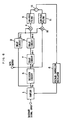
- Fig. 1 is a block diagram showing the structure of a data reproducing unit according to a first embodiment of the present invention.
- Fig. 2 is a block diagram showing the structure of a data transmission system from a modulation part 31 to a demodulation part 33, which is arranged in front of the data reproducing unit shown in Fig. 1.
- Figs. 3(a) to 3(c) are waveform diagrams of signals from respective parts in Fig. 2.
- Transmission symbols (see Fig. 3(a)) which are inputted in the modulation part 31 in Fig. 2 are converted to a continuous waveform through band limitation of the modulation part 31, then transmitted through a transmission line 32, subjected to receiving-side band limitation in the demodulation part 33, and supplied to the data reproducing unit shown in Fig. 1.
- the modulation part 31 and the demodulation part 33 handle only the signal of the base band width.
- the modulation part 31 performs conversion from the base band width to the carrier band width, while the demodulation part 32 performs the conversion vice versa.
- total transmission characteristics of the modulation part 31, the transmission line 32 and the demodulation part 33 have impulse response of a full roll-off filter illustrated in Fig. 4, and hence the output of the demodulation part 33 has a continuous waveform shown in Fig. 3(b).
- Data can be correctly reproduced by sampling this continuous waveform in synchronization with a clock (see Fig. 3(c)) having the same timing as the transmission symbol which is inputted in the modulation part 31.
- a clock see Fig. 3(c)
- the data reproducing unit comprises a sampler 1, a decision circuit 2, a delay circuit 3, a multiplier 4, a low-pass filter 5, and a voltage controlled oscillator 6.
- the sampler 1 samples an inputted base band signal in accordance with a sampling clock which is supplied from the voltage controlled oscillator 6, and outputs a sample value S n .
- the decision circuit 2 determines the sample value S n , and outputs data d n which is an estimate value of the transmission symbol.
- the delay circuit 3 delays the data d n by one sampling clock, and outputs data d n-1 .
- the multiplier 4 multiplies the sample value S n by the delayed data d n-1 .
- the low-pass filter 5 smoothes the output of the multiplier 4, and extracts its dc component.
- the voltage controlled oscillator 6 generates the sampling clock having a changeable frequency according to the sign and the magnitude of the dc component.
- Fig. 5 shows sample values upon shift of a sampling clock from the optimum position.
- sample values A and D are larger than the original values in Fig. 3(b).
- data X1 and X4 which are precedent to A and D are positive in polarity and sampling timings approach the precedent data so that the response from the precedent data is positive similarly to the polarity thereof.
- the response from precedent data X5 and X6 is negative similarly to the polarity thereof, and hence the sample values are smaller than the original values.
- sample values a and d are smaller than the original values in Fig. 3(b).
- the data X1 and X4 which are precedent to a and d are positive in polarity and the sampling timings are separated from the precedent data, so that the response from the precedent is negative reversely to the polarity thereof.
- the response from the precedent data X5 and X6 is positive reversely to the polarity thereof, and hence the sample values are larger than the original values.
- the multiplier 4 multiplies sample values by data which are precedent thereto, and the low-pass filter 5 approximately accumulates the results of such multiplication, thereby outputting correlation values thereof in consequence.
- the voltage controlled oscillator 6 has such characteristics that the frequency is reduced when the control voltage is increased, and vice versa.
- a sampling timing is premature, the correlation is positive and hence the control voltage is increased while the sampling frequency is reduced. Consequently, the sampling timing is delayed.
- the sampling timing is late, on the other hand, the correlation is negative, and hence the control voltage is reduced while the sampling frequency is increased. Consequently, the sampling timing is brought forward.
- the sampling timing is controlled so that the correlation is zero, thereby achieving sampling at the optimum time.
- S n k ⁇ a n+1 h(t - T) + a n h(t) + a n-1 (t + T) ⁇
- k represents the total amplitude gain of the modulation part 31, the transmission part 32 and the demodulation part 33
- h( ) represents the impulse response of the total transmission characteristics of the modulation part 31, the transmission part 32 and the demodulation part 33
- a n represents data transmitted from the modulation part
- a n+1 represents data which is subsequent thereto
- a n-1 represents data which is precedent thereto
- t represents a shifted time from the optimum sampling timing
- T represents one symbol length.
- the decision circuit 2 outputs the decision value d n of S n , and the delay circuit 3 delays the same by one sample and outputs d n-1 .
- a timing error signal of the above equation (5) is passed through the low-pass filter 8, so that its low frequency component, i.e., an average value, is obtained.
- the sample value may alternatively be delayed for obtaining the correlation between the sample value and data which is subsequent thereto.
- the control voltage is reduced when the sampling timing is premature since the correlation is negative, while the control voltage is increased when the sampling timing is late since the correlation is positive. Therefore, sampling at the optimum time is realized by providing the voltage controlled oscillator 6 with such characteristics that the frequency is increased when the control voltage is increased, and vice versa.
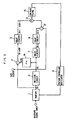
- Fig. 6 is a block diagram showing the structure of a data reproducing unit according to a second embodiment of the present invention.
- the embodiment shown in Fig. 6 is formed as a data reproducing unit corresponding to a transmission symbol which is not completely at random.
- this data reproducing unit comprises a sampler 1, a decision circuit 2, multipliers 4 and 10, low-pass filters 5 and 11, a voltage controlled oscillator 6, delay circuits 7 to 9, and a subtracter 12.
- the sampler 1 samples an inputted base band signal in accordance with a sampling clock which is supplied from the voltage controlled oscillator 6, and outputs a sample value S n .
- the decision circuit 2 determines the sample value S n , and outputs data d n which is an estimate value of the transmission symbol.
- the delay circuit 7 delays the data d n by one sampling clock, and outputs data d n-1 .
- the delay circuit 8 delays the data d n-1 by one sampling clock, and outputs data d n-2 .
- the delay circuit 9 delays the sample value S n by one sampling clock, and outputs a sample value S n-1 .
- the multiplier 4 multiplies the sample value S n-1 by the data d n-2 .
- the low-pass filter 5 smoothes the output of the multiplier 4, and extracts its dc component.
- the multiplier 10 multiplies the sample value S n-1 by the data d n .
- the low-pass filter 11 smoothes the output of the multiplier 10, and extracts its dc component.
- the subtracter 12 subtracts the dc component outputted from the low-pass filter 11 from that outputted from the low-pass filter 5.
- the voltage controlled oscillator 6 generates the sampling clock having a changeable frequency according to the sign and the magnitude of the output signal from the subtracter 12.
- the reason why the base band signal can be sampled at the optimum timing by the structure shown in Fig. 6 is now described in detail.
- the subtracter 12 subtracts the correlation between a sample value and data subsequent thereto from that between the sample value and data precedent thereto, whereby its output is positive when the sampling timing shifts forwardly, and vice versa.
- the voltage controlled oscillator 6 is controlled by the output of the subtracter 12, whereby sampling at the optimum time can be implemented similarly to the first embodiment. Further, the voltage controlled oscillator 6 can be more correctly controlled, due to the difference between two correlation values.
- All of the multipliers 4 and 5, the low-pass filters 5 and 11 and the subtracter 12 shown in Fig. 6 perform linear processing on the data d n-2 and d n .
- the subtracter may first subtract the data d n from the data d n-2 , and then a multiplier and a low-pass filter are provided.
- the data reproducing unit has a structure shown in Fig. 7, whereby the numbers of the multipliers and the low-pass filters can be reduced.
- a subtracter 13 subtracts data d n from data d n-2 .
- a multiplier 14 multiplies the output of the subtracter 13 by a sample value S n-1 . It will be confirmed with equations that the voltage controlled oscillator 6 can be more correctly controlled with the structure shown in Fig. 7 as compared with the first embodiment.
- a timing error signal of the above equation (10) is passed through a low-pass filter 15, so that its low frequency component, i.e., an average value, is obtained.
- the position of the sampling clock is controlled through the correlation between the sample value of the base band signal and the data adjacent thereto.
- the correlation between an error included in a base band signal and data adjacent thereto is utilized, on the other hand, the position of the sampling clock can be more correctly controlled.
- Fig. 8 is a block diagram showing the structure of a data reproducing unit according to a fourth embodiment of the present invention.
- this data reproducing unit comprises a sampler 1, a decision circuit 2, a delay circuit 3, a multiplier 4, a low-pass filter 5, a voltage controlled oscillator 6, a constant multiplier 16, and a subtracter 17.
- the sampler 1 samples an inputted base band signal in accordance with a sampling clock which is supplied from the voltage controlled oscillator 6, and outputs a sample value S n .
- the decision circuit 2 determines the sample value S n , and outputs data d n which is an estimate value of the transmission symbol.
- the delay circuit 3 delays the data d n by one sampling clock, and outputs data d n-1 .
- the constant multiplier 16 multiplies the data d n by a constant ⁇ , and outputs ⁇ d n .
- the subtracter 17 subtracts ⁇ d n from the sample value S n .
- the multiplier 4 multiplies the output of the subtracter 17 by the delayed data d n-1 .
- the low-pass filter smoothes the output of the multiplier 4, and extracts its dc component.
- the voltage controlled oscillator 6 generates the sampling clock having a changeable frequency, according to the sign and the magnitude of the dc component.
- the reason why the base band signal can be sampled at the optimum timing with the structure shown in Fig. 8 is now described in detail.
- the basic structure is identical to the structure shown in Fig. 1 illustrated with reference to the first embodiment, and hence a part different from this structure is described with an equation.
- the correlation value outputted from the low-pass filter 5 is expressed in the equation (8), similarly to the first embodiment.
- the term ka n d n-1 is replaced with (ka n - ⁇ d n )d n-1 .
- This term which is irrelevant to the shifted time t of the sampling timing, is preferably minimized, in order to detect the shifted time for employing the same for control.
- d n may be regarded as being equal to a n , and hence the absolute value of this term can be reduced by selecting the multiplication constant ⁇ at a value which is close to the total gain k.
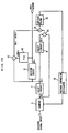
- Fig. 9 is a block diagram showing the structure of a data reproducing unit according to a fifth embodiment of the present invention.
- this data reproducing unit comprises a sampler 1, a decision circuit 2, a voltage controlled oscillator 6, delay circuits 7 to 9, a subtracter 13, a multiplier 14, a low-pass filter 15, a constant multiplier 16, and a subtracter 17.
- the sampler 1 samples an inputted base band signal in accordance with a sampling clock which is supplied from the voltage controlled oscillator 6, and outputs a sample value S n .
- the decision circuit 2 determines the sample value S n , and outputs data d n which is an estimate value of the transmission symbol.
- the delay circuit 7 delays the data d n by one sampling clock, and outputs data d n-1 .
- the delay circuit 8 delays the data d n-1 by one sampling clock, and outputs data d n-2 .
- the subtracter 13 subtracts the data d n from the data d n-2 , and outputs d n-2 - d n .
- the constant multiplier 16 multiplies the data d n by a constant ⁇ , and outputs ⁇ d n .
- the subtracter 17 subtracts ⁇ d n from the sample value S n , and outputs S n - ⁇ d n .
- the delay circuit 9 delays S n - ⁇ d n by one sampling clock, and outputs S n-1 - ⁇ d n-1 .
- the multiplier 14 multiplies S n-1 - ⁇ d n-1 by d n-2 - d n .
- the low-pass filter 15 smoothes the output of the multiplier 14, and extracts its dc component.
- the voltage controlled oscillator 6 generates the sampling clock having a changeable frequency, according to the sign and the magnitude of the dc component.
- the correlation value outputted from the low-pass filter 15 is expressed in the equation (13), similarly to the third embodiment.
- the term ka n-1 (d n-2 - d n ) is replaced with (ka n-1 - ⁇ d n-1 )(d n-2 - d n ).
- This term which is irrelevant to the shifted time t of the sampling timing, is preferably minimized in order to detect the shifted time and employ the same for control.
- d n may be regarded as being equal to an, and hence the absolute value of this term can be reduced by selecting the multiplication constant ⁇ at a value which is close to the total gain k.
- Each of the fourth and fifth embodiments is adapted to control the position of the sampling clock through the correlation between an error included in the base band signal and data adjacent thereto.
- the correlation between an error included in a base band signal and a sample value of a base band signal which is adjacent thereto can be utilized.
- the relation between the correlation value and sampling clock shift is maintained even if carrier reproduction of a carrier transmission system is so incomplete that the base band signal is mixed with another base band signal, whereby the position of the sampling clock can be correctly controlled.
- Fig. 10 is a block diagram showing the structure of a data reproducing unit according to a sixth embodiment of the present invention.
- this data reproducing unit comprises a sampler 1, a decision circuit 2, a delay circuit 3, a multiplier 4, a low-pass filter 5, a voltage controlled oscillator 6, a constant multiplier 16, and a subtracter 17.
- the sampler 1 samples an inputted base band signal in accordance with a sampling clock which is supplied from the voltage controlled oscillator 6, and outputs a sample value S n .
- the decision circuit 2 determines the sample value S n , and outputs data d n which is an estimate value of the transmission symbol.
- the constant multiplier 16 multiplies the data d n by a constant ⁇ , and outputs ⁇ d n .
- the subtracter 17 subtracts ⁇ d n from the sample value S n .
- the delay circuit 3 delays the sample value S n by one sampling clock, and outputs a sample value S n-1 .
- the multiplier 4 multiplies the output of the subtracter 17 by the delayed sample value S n-1 .
- the low-pass filter 5 smoothes the output of the multiplier 4, and extracts its dc component.
- the voltage controlled oscillator 6 generates the sampling clock having a changeable frequency, according to the sign and the magnitude of the dc component.
- equation (16) reflects the sign and the magnitude of the shifted time t.
- Fig. 11 is a block diagram showing the structure of a data reproducing unit according to a seventh embodiment of the present invention.
- this data reproducing unit comprises a sampler 1, a decision circuit 2, a voltage controlled oscillator 6, delay circuits 7 to 9, a subtracter 13, a multiplier 14, a low-pass filter 15, a constant multiplier 16, and a subtracter 17.
- the sampler 1 samples an inputted base band signal in accordance with a sampling clock which is supplied from the voltage controlled oscillator 6, and outputs a sample value S n .
- the decision circuit 2 determines the sample value S n , and outputs data d n which is an estimate value of the transmission symbol.
- the delay circuit 7 delays the sample value S n by one sampling clock, and outputs a sample value S n-1 .
- the delay circuit 8 delays the sample value S n-1 by one sampling clock, and outputs a sample value S n-2 .
- the subtracter 13 subtracts the sample value S n from the sample value S n-2 , and outputs S n-2 - S n .
- the constant multiplier 16 multiplies the data d n by a constant ⁇ , and outputs ⁇ d n .
- the subtracter 17 subtracts ⁇ d n from the sample value S n , and outputs S n - ⁇ d n .
- the delay circuit 9 delays S n - ⁇ d n by one sampling clock, and outputs S n-1 - ⁇ ds n-1 .
- the multiplier 14 multiplies S n-1 - ⁇ d n-1 by S n-2 - S n .
- the low-pass filter 15 smoothes the output of the multiplier 14, and extracts its dc component.
- the voltage controlled oscillator 6 generates the sampling clock having a changeable frequency, according to the sign and the magnitude of the dc component.
- equation (17) reflects the sign and the magnitude of the shifted time t.
- S n-1 - ⁇ d n-1 in order to obtain S n-1 - ⁇ d n-1 to be supplied to the multiplier 14, S n - ⁇ d n is first produced by the constant multiplier 16 and the subtracter 17, and delayed by the delay circuit 9.
- S n-1 - ⁇ d n-1 can be obtained by applying the constant multiplier 16 and the subtracter 17 to S n-1 which is outputted from the delay circuit 7.
- Fig. 12 shows this structure as an eighth embodiment. When the structure shown in Fig. 12 is employed, the delay circuit 9 shown in Fig. 11 can be omitted.
- Fig. 13 is a block diagram showing the structure of a data reproducing unit according to a ninth embodiment of the present invention.
- the base band signal input of the eighth embodiment shown in Fig. 12 is extended to two.
- samplers 1a and 1b, decision circuits 2a and 2b, delay circuits 7a and 7b, delay circuits 8a and 8b, subtracters 13a and 13b, multipliers 14a and 14b, constant multipliers 16a and 16b and subtracters 17a and 17b are identical in structure to the sampler 1, the decision circuit 2, the delay circuit 7, the delay circuit 8, the subtracter 13, the multiplier 14, the constant multiplier 16 and the subtracter 17 of the eighth embodiment (Fig. 12) respectively, and hence redundant description is omitted.
- the data reproducing unit shown in Fig. 13 further comprises a voltage controlled oscillator 6, a low-pass filter 15, and an adder 18.
- the sampler 1a samples an inputted first base band signal in accordance with a sampling clock which is supplied from the voltage controlled oscillator 6.
- the subsequent operations up to the multiplier 14a are identical to that of the eighth embodiment.
- the sampler 1b samples an inputted second base band signal in accordance with a sampling clock which is supplied from the voltage controlled oscillator 6.
- the subsequent operations up to the multiplier 14b are identical to that of the eighth embodiment.
- the adder 18 adds up timing error signals which are outputted from the multipliers 14a and 14b respectively with each other.
- the low-pass filter 15 extracts a low frequency component from the result of the addition, and supplies a control voltage to the voltage controlled oscillator 6.
- the voltage controlled oscillator 6 outputs the clock having a frequency depending on the control voltage, and supplies the same to the samplers 1a and 1b as the sampling clock.
- both of the timing error signals obtained from the two base band inputs are employed for controlling the sampling timing. Therefore, the amount of disturbance of the sampling timing caused by noises included in the base band signals is reduced as compared with the case of utilizing only one base band signal.
- the base band signal can be extended to at least two also as to each of the first to seventh embodiments, similarly to the case of the ninth embodiment.
- the sampler may be implemented by an A/D converter.
- the subsequent delay circuit can be readily implemented by a flip-flop or the like while the arithmetic circuit such as the subtracter can also be implemented by a digital circuit, whereby a data reproducing unit which is suitable for integration can be obtained.
Landscapes
- Engineering & Computer Science (AREA)
- Computer Networks & Wireless Communication (AREA)
- Signal Processing (AREA)
- Synchronisation In Digital Transmission Systems (AREA)
- Digital Transmission Methods That Use Modulated Carrier Waves (AREA)
- Dc Digital Transmission (AREA)
- Stabilization Of Oscillater, Synchronisation, Frequency Synthesizers (AREA)
Claims (10)
- Datenrückgewinnungseinheit zum Rückgewinnen von Originaldaten aus einem Abtastwert, erhalten durch Abtasten eines Eingangssignals von einem Datenübertragungssystem, welches einen Modulationsteil (31), einen Übertragungspfad (32) und einen Demodulationsteil (33) beinhaltet, wo die Gesamtübertragungscharakteristik des Modulationsteils (31), des Übertragungspfads (32) und des Demodulationsteils (33) nur eine Art von Impulsantwort hat, wobei die Datenrückgewinnungseinheit umfasst:worin die Takterzeugungsmittel eine Phase des Abtasttakts anpassen in Übereinstimmung mit einer Polarität des jeweiligen ersten, zweiten oder dritten Korrelationswerts.Takterzeugungsmittel (6) zum Erzeugen eines Abtasttakts;einen Abtaster (1) zum Abtasten des Eingangssignals in Übereinstimmung mit dem Abtasttakt, um einen ersten Abtastwert auszugeben;eine Entscheidungsschaltung (2) zum, basierend auf dem ersten Abtastwert ausgegeben von dem Abtaster, Ausgeben eines ersten Schätzwerts einesÜbertragungssymbols als die Originaldaten; und eines der Mittel (3 bis 5, 7 bis 18) zum:Berechnen eines ersten Korrelationswerts basierend auf dem ersten Abtastwert und einem zweiten Schätzwert, der erhalten wird durch Verschieben des ersten Schätzwerts um ein Symbol auf der Zeitachse, wobei der erste Korrelationswert eine Richtung repräsentiert, in welcher das Abtast-Timing verschoben wird;Berechnen eines zweiten Korrelationswerts basierend auf einem Wert, der erhalten wird durch Subtrahieren eines konstanten Vielfachen des ersten Schätzwerts von dem ersten Abtastwert und einem zweiten Schätzwert, der erhalten wird durch Verschieben des ersten Schätzwerts um ein Symbol auf der Zeitachse, wobei der zweite Korrelationswert eine Richtung repräsentiert, in welcher das Abtast-Timing verschoben wird; oderBerechnen eines dritten Korrelationswerts basierend auf einem Wert, der erhalten wird durch Subtrahieren eines konstanten Vielfachen des ersten Schätzwerts von dem ersten Abtastwert und einem zweiten Abtastwert, der erhalten wird durch Verschieben des ersten Abtastwerts um ein Symbol auf der Zeitachse, wobei der dritte Korrelationswert eine Richtung repräsentiert, in welcher das Abtast-Timing verschoben wird,
- Datenrückgewinnungseinheit nach Anspruch 1, worin
die Entscheidungsschaltung (2) den ersten Schätzwert (dn) als die Originaldaten ausgibt durch Bestimmen des ersten Abtastwerts (Sn),und
das Mittel zum Berechnen entweder des ersten, zweiten oder dritten Korrelationswerts beinhaltet:eine Verzögerungsschaltung (3) zum Ausgeben des zweiten Schätzwerts (dn-1) durch Verschieben des ersten Schätzwertes (dn) um ein Symbol auf der Zeitachse;einen Multiplizierer (4) zum Ausgeben eines Ergebnisses des Multiplizierens des ersten Abtastwerts (Sn), ausgegeben von dem Abtaster (1), mit dem zweiten Schätzwert (dn-1), ausgegeben von der Verzögerungsschaltung (3); undein Tiefpassfilter (5) zum Durchleiten einer niederfrequenten Komponente der Ausgabe des Multiplizierers, um die niederfrequente Komponente als den ersten Korrelationswert auszugeben. - Datenrückgewinnungseinheit nach Anspruch 1, worin
die Entscheidungsschaltung (2) den ersten Schätzwert (dn) als die Originaldaten ausgibt durch Bestimmen des ersten Abtastwerts (Sn) und das Mittel zum Berechnen entweder des ersten, zweiten oder dritten Korrelationswerts beinhaltet:eine erste Verzögerungsschaltung (7) zum Ausgeben eines zweiten Schätzwerts (dn-1) durch Verschieben des ersten Schätzwerts (dn) um ein Symbol auf der Zeitachse;eine zweite Verzögerungsschaltung (8) zum Ausgeben eines dritten Schätzwerts (dn-2) durch Verschieben des zweiten Schätzwertes (dn-1), ausgegeben von der ersten Verzögerungsschaltung (7), um ein Symbol auf der Zeitachse;eine dritte Verzögerungsschaltung (9) zum Ausgeben eines zweiten Abtastwerts (Sn-1) durch Verschieben des ersten Abtastwerts (Sn), ausgegeben von dem Abtaster (1), um ein Symbol auf der Zeitachse;einen ersten Multiplizierer (4) zum Ausgeben eines Ergebnisses des Multiplizierens des zweiten Abtastwerts (Sn-1), ausgegeben von der dritten Verzögerungsschaltung (9), mit dem dritten Schätzwert (dn-2), ausgegeben von der zweiten Verzögerungsschaltung (8);einen zweiten Multiplizierer (10) zum Ausgeben eines Ergebnisses des Multiplizierens des zweiten Abtastwerts (Sn-1), ausgegeben von der dritten Verzögerungsschaltung (9), mit dem ersten Schätzwert (dn), ausgegeben von der Entscheidungsschaltung (2),ein erstes Tiefpassfilter (5) zum Durchleiten einer niederfrequenten Komponente der Ausgabe des ersten Multiplizierers (4);ein zweites Tiefpassfilter (11) zum Durchleiten einer niederfrequenten Komponente der Ausgabe des zweiten Multiplizierers (10); undeinen Subtrahierer (12) zum Ausgeben, als den ersten Korrelationswert, eines Ergebnisses des Subtrahierens einer dc-Komponente, welche von dem zweiten Tiefpassfilter (11) ausgegeben wird, von einer dc-Komponente, welche von dem ersten Tiefpassfilter (5) ausgegeben wird. - Datenrückgewinnungseinheit nach Anspruch 1, worin
die Entscheidungsschaltung (2) den ersten Schätzwert (dn) als die Originaldaten ausgibt durch Bestimmen des ersten Abtastwerts (Sn), und
das Mittel zum Berechnen entweder des ersten, zweiten oder dritten Korrelationswerts beinhaltet:ein Tiefpassfilter (15) zum Durchleiten einer niederfrequenten Komponente der Ausgabe des Multiplizierers (14); und Ausgeben der niederfrequenten Komponente als dem ersten Korrelationswert.eine erste Verzögerungsschaltung (7) zum Ausgeben eines zweiten Schätzwerts (dn-1) durch Verschieben des ersten Schätzwerts (dn) um ein Symbol auf der Zeitachse;eine zweite Verzögerungsschaltung (8) zum Ausgeben eines dritten Schätzwerts (dn-2) durch Verschieben des zweiten Schätzwerts (dn-1), ausgegeben von der ersten Verzögerungsschaltung (7), um ein Symbol auf der Zeitachse;eine dritte Verzögerungsschaltung (9) zum Ausgeben eines zweiten Abtastwerts (Sn-1) durch Verschieben des ersten Abtastwerts (Sn), ausgegeben von dem Abtaster (1), um ein Symbol auf der Zeitachse;einen Subtrahierer (13) zum Ausgeben eines Ergebnisses des Subtrahierens des ersten Schätzwerts (dn) von dem dritten Schätzwert (dn-2);einen Multiplizierer (14) zum Ausgeben eines Ergebnisses des Multiplizierens des zweiten Abtastwerts (Sn-1), ausgegeben von der dritten Verzögerungsschaltung (9) mit der Ausgabe des Subtrahierers (13); und - Datenrückgewinnungseinheit nach Anspruch 1, worin
die Entscheidungsschaltung (2) den ersten Schätzwert (dn) als die Originaldaten ausgibt durch Bestimmen des ersten Abtastwerts (Sn), und
das Mittel zum Berechnen entweder des ersten, zweiten oder dritten Korrelationswerts beinhaltet:ein Tiefpassfilter (5) zum Durchleiten einer niederfrequenten Komponente der Ausgabe des Multiplizierers (4), und Ausgeben der niederfrequenten Komponente als dem zweiten Korrelationswert.eine Verzögerungsschaltung (3) zum Ausgeben des zweiten Schätzwerts (dn-1) durch Verschieben des ersten Schätzwerts (dn) um ein Symbol auf der Zeitachse;einen Konstantenmultiplizierer (16) zum Ausgeben eines Ergebnisses des Multiplizierens des ersten Schätzwerts (dn) mit einer Konstanten (α),einen Subtrahierer (17) zum Ausgeben eines Ergebnisses des Subtrahierens der Ausgabe des Konstantenmultiplizierers (αdn) von dem ersten Abtastwert (Sn);einen Multiplizierer (4) zum Ausgeben eines Ergebnisses des Multiplizierens der Ausgabe des Subtrahierers (17) mit dem zweiten Schätzwert (dn-1), ausgegeben von der Verzögerungsschaltung (3); und - Datenrückgewinnungseinheit nach Anspruch 1, worin
die Entscheidungsschaltung (2) den ersten Schätzwert (dn) als die Originaldaten ausgibt durch Bestimmen des ersten Abtastwerts (Sn), und
das Mittel zum Berechnen entweder des ersten, zweiten oder dritten Korrelationswerts beinhaltet:ein Tiefpassfilter (15) zum Durchleiten einer niederfrequenten Komponente der Ausgabe des Multiplizierers (14), und Ausgeben der niederfrequenten Komponente als dem zweiten Korrelationswert.eine erste Verzögerungsschaltung (7) zum Ausgeben eines zweiten Schätzwerts (dn-1) durch Verschieben des ersten Schätzwerts (dn) um ein Symbol auf der Zeitachse;eine zweite Verzögerungsschaltung (8) zum Ausgeben eines dritten Schätzwerts (dn-2) durch Verschieben des zweiten Schätzwerts (dn-1), ausgegeben von der ersten Verzögerungsschaltung (7), um ein Symbol auf der Zeitachse;einen ersten Subtrahierer (13) zum Ausgeben eines Ergebnisses des Subtrahierens des ersten Schätzwerts (dn), ausgegeben von der Entscheidungsschaltung (2), von dem dritten Schätzwert (dn-2), ausgegeben von der zweiten Verzögerungsschaltung (8);einen Konstantenmultiplizierer (16) zum Ausgeben eines Ergebnisses des Multiplizierens des ersten Schätzwerts (dn) mit einer Konstanten (α),einen zweiten Subtrahierer (17) zum Ausgeben eines Ergebnisses des Subtrahierens der Ausgabe (αdn) des Konstantenmultiplizierers (16) von dem ersten Abtastwert (Sn);eine dritte Verzögerungsschaltung (9) zum Verschieben der Ausgabe (Sn-αdn) des zweiten Subtrahierers um ein Symbol auf der Zeitachse;einen Multiplizierer (14) zum Ausgeben eines Ergebnisses des Multiplizierens der Ausgabe der dritten Verzögerungsschaltung (9) mit der Ausgabe des ersten Subtrahierers (13); und - Datenrückgewinnungseinheit nach Anspruch 1, worin
die Entscheidungsschaltung (2) den ersten Schätzwert (dn) als die Originaldaten ausgibt durch Bestimmen des ersten Abtastwerts (Sn), und
das Mittel zum Berechnen entweder des ersten, zweiten oder dritten Korrelationswerts beinhaltet:eine Verzögerungsschaltung (3) zum Ausgeben des zweiten Abtastwerts (Sn-1) durch Verschieben des ersten Abtastwerts (Sn) um ein Symbol auf der Zeitachse;einen Konstantenmultiplizierer (16) zum Ausgeben eines Ergebnisses des Multiplizierens des ersten Schätzwerts (dn) mit einer Konstanten (α),einen Subtrahierer (17) zum Ausgeben eines Ergebnisses des Subtrahierens der Ausgabe des Konstantenmultiplizierers (αdn) von dem ersten Abtastwert (Sn);einen Multiplizierer (4) zum Ausgeben eines Ergebnisses des Multiplizierens der Ausgabe des Subtrahierers (17) mit dem zweiten Abtastwert (Sn-1), ausgegeben von der Verzögerungsschaltung (3); und
ein Tiefpassfilter (5) zum Durchleiten einer niederfrequenten Komponente der Ausgabe des Multiplizierers (4), und Ausgeben der niederfrequenten Komponente als dem dritten Korrelationswert. - Datenrückgewinnungseinheit nach Anspruch 1, worin
die Entscheidungsschaltung (2) den ersten Schätzwert (dn) als die Originaldaten ausgibt durch Bestimmen des ersten Abtastwerts (Sn), und
das Mittel zum Berechnen entweder des ersten, zweiten oder dritten Korrelationswerts beinhaltet:eine erste Verzögerungsschaltung (7) zum Ausgeben eines zweiten Abtastwerts (Sn-1) durch Verschieben des ersten Abtastwerts (Sn) um ein Symbol auf der Zeitachse;eine zweite Verzögerungsschaltung (8) zum Ausgeben eines dritten Abtastwerts (Sn-2) durch Verschieben des zweiten Abtastwerts (Sn-1), ausgegeben von der ersten Verzögerungsschaltung (7), um ein Symbol auf der Zeitachse;einen ersten Subtrahierer (13) zum Ausgeben eines Ergebnisses des Subtrahierens des ersten Abtastwerts (Sn) von dem dritten Abtastwert (Sn-2);einen Konstantenmultiplizierer (16) zum Ausgeben eines Ergebnisses des Multiplizierens des ersten Schätzwerts (dn) mit einer Konstanten (α),einen zweiten Subtrahierer (17) zum Ausgeben eines Ergebnisses des Subtrahierens der Ausgabe (αdn) des Konstantenmultiplizierers (16) von dem ersten Abtastwert (Sn);eine dritte Verzögerungsschaltung (9) zum Verschieben der Ausgabe des zweiten Subtrahierers (17) um ein Symbol auf der Zeitachse; einen Multiplizierer (14) zum Ausgeben eines Ergebnisses des Multiplizierens der Ausgabe der dritten Verzögerungsschaltung (9) mit der Ausgabe des ersten Subtrahierers (13); und
ein Tiefpassfilter (15) zum Durchleiten einer niederfrequenten Komponente der Ausgabe des Multiplizierers (14), und Ausgeben der niederfrequenten Komponente als dem dritten Korrelationswert. - Datenrückgewinnungseinheit nach Anspruch 1, worin
die Entscheidungsschaltung (2) den ersten Schätzwert (dn-1) als die Originaldaten ausgibt durch Bestimmen des zweiten Abtastwerts (Sn-1), erhalten durch Verschieben des ersten Abtastwerts (Sn) um ein Symbol auf der Zeitachse,
das Mittel zum Berechnen entweder des ersten, zweiten oder dritten Korrelationswerts beinhaltet:eine erste Verzögerungsschaltung (7) zum Ausgeben eines zweiten Abtastwerts (Sn-1) durch Verschieben des ersten Abtastwerts (Sn) um ein Symbol auf der Zeitachse;eine zweite Verzögerungsschaltung (8) zum Ausgeben eines dritten Abtastwerts (Sn-2) durch Verschieben des zweiten Abtastwerts (Sn-1), ausgegeben von der ersten Verzögerungsschaltung (7), um ein Symbol auf der Zeitachse;einen ersten Subtrahierer (13) zum Ausgeben eines Ergebnisses des Subtrahierens des ersten Abtastwerts (Sn) von dem dritten Abtastwert (Sn-2);einen Konstantenmultiplizierer (16) zum Ausgeben eines Ergebnisses des Multiplizierens des ersten Schätzwerts (dn-1) mit einer Konstanten (α),einen zweiten Subtrahierer (17) zum Ausgeben eines Ergebnisses des Subtrahierens der Ausgabe (αdn-1) des Konstantenmultiplizierers (16) von dem zweiten Abtastwert (Sn-1);einen Multiplizierer (14) zum Ausgeben eines Ergebnisses des Multiplizierens der Ausgabe des zweiten Subtrahierers (17) mit der Ausgabe des ersten Subtrahierers (13); und
ein Tiefpassfilter (15) zum Durchleiten einer niederfrequenten Komponente der Ausgabe des Multiplizierers (14), und Ausgeben der niederfrequenten Komponente als dem dritten Korrelationswert. - Datenrückgewinnungseinheit nach Anspruch 1, worin der Abtaster umfasst:die Entscheidungsschaltung umfasst:einen ersten Abtaster (1a) zum Ausgeben des ersten Abtastwerts durch Abtasten eines ersten Basisbandsignals;einen zweiten Abtaster (1b) zum Ausgeben eines vierten Abtastwerts durch Abtasten eines zweiten Basisbandsignals;das Mittel zum Berechnen entweder des ersten, zweiten oder dritten Korrelationswerts beinhaltet:eine erste Entscheidungsschaltung (2a) zum Ausgeben des ersten Schätzwerts als erste Originaldaten durch Bestimmen des zweiten Abtastwerts, erhalten durch Verschieben des ersten Abtastwerts um ein Symbol auf der Zeitachse; undeine zweite Entscheidungsschaltung (2b) zum Ausgeben des zweiten Schätzwerts als zweite Originaldaten durch Bestimmen eines fünften Abtastwerts erhalten durch Verschieben des vierten Abtastwerts um ein Symbol auf der Zeitachse, undein Tiefpassfilter (15) zum Durchleiten einer niederfrequenten Komponente der Ausgabe des Addierers (18), und Ausgeben der niederfrequenten Komponente als dem dritten Korrelationswert.eine erste Verzögerungsschaltung (7a) zum Ausgeben eines zweiten Abtastwerts durch Verschieben des ersten Abtastwerts um ein Symbol auf der Zeitachse;eine zweite Verzögerungsschaltung (8a) zum Ausgeben eines dritten Abtastwerts durch Verschieben des zweiten Abtastwerts, ausgegeben von der ersten Verzögerungsschaltung (7a), um ein Symbol auf der Zeitachse;einen ersten Subtrahierer (13a) zum Ausgeben eines Ergebnisses des Subtrahierens des ersten Abtastwerts von dem dritten Abtastwert;einen ersten Konstantenmultiplizierer (16a) zum Ausgeben eines Ergebnisses des Multiplizierens des ersten Schätzwerts mit einer Konstanten,einen zweiten Subtrahierer (17a) zum Ausgeben eines Ergebnisses des Subtrahierens der Ausgabe des ersten Konstantenmultiplizierers von dem ersten Abtastwert;einen ersten Multiplizierer (14a) zum Ausgeben eines Ergebnisses des Multiplizierens der Ausgabe des zweiten Subtrahierers (17a) und der Ausgabe des ersten Subtrahierers (13a)eine dritte Verzögerungsschaltung (7b) zum Ausgeben eines fünften Abtastwerts durch Verschieben des vierten Abtastwerts um ein Symbol auf der Zeitachse;eine vierte Verzögerungsschaltung (8b) zum Ausgeben eines sechsten Abtastwerts durch Verschieben des fünften Abtastwerts, ausgegeben von der dritten Verzögerungsschaltung (7b), um ein Symbol auf der Zeitachse;einen dritten Subtrahierer (13b) zum Ausgeben eines Ergebnisses des Subtrahierens des vierten Abtastwerts von dem sechsten Abtastwert;einen Konstantenmultiplizierer (16b) zum Ausgeben eines Ergebnisses des Multiplizierens des zweiten Schätzwertes mit einer Konstanten;einen vierten Subtrahierer (14b) zum Ausgeben eines Ergebnisses des Subtrahierens der Ausgabe des zweiten Konstantenmultiplizierers von dem fünften Abtastwerts;einen zweiten Multiplizierer (14b) zum Ausgeben eines Ergebnisses des Multiplizierens der Ausgabe des vierten Subtrahierers (17b) und der Ausgabe des dritten Subtrahierers (13b);einen Addierer (18) zum Ausgeben eines Ergebnisses des Addierens der Ausgabe des ersten Multiplizierers (14a) zu der Ausgabe des zweiten Multiplizierers (14b); und
Applications Claiming Priority (3)
| Application Number | Priority Date | Filing Date | Title |
|---|---|---|---|
| JP36783/95 | 1995-02-24 | ||
| JP03678395A JP3382745B2 (ja) | 1995-02-24 | 1995-02-24 | データ再生方法およびデータ再生装置 |
| JP3678395 | 1995-02-24 |
Publications (3)
| Publication Number | Publication Date |
|---|---|
| EP0729251A2 EP0729251A2 (de) | 1996-08-28 |
| EP0729251A3 EP0729251A3 (de) | 1999-08-18 |
| EP0729251B1 true EP0729251B1 (de) | 2005-04-20 |
Family
ID=12479383
Family Applications (1)
| Application Number | Title | Priority Date | Filing Date |
|---|---|---|---|
| EP96102666A Expired - Lifetime EP0729251B1 (de) | 1995-02-24 | 1996-02-22 | Anordnung zur Datenwiedergabe mit Zeitabtastung |
Country Status (4)
| Country | Link |
|---|---|
| US (1) | US5778032A (de) |
| EP (1) | EP0729251B1 (de) |
| JP (1) | JP3382745B2 (de) |
| DE (1) | DE69634621T2 (de) |
Families Citing this family (6)
| Publication number | Priority date | Publication date | Assignee | Title |
|---|---|---|---|---|
| WO1998009400A1 (en) * | 1996-08-30 | 1998-03-05 | International Business Machines Corporation | Receiving and equalizing signals for high-speed data transmission |
| US6178316B1 (en) * | 1997-04-29 | 2001-01-23 | Meta-C Corporation | Radio frequency modulation employing a periodic transformation system |
| DE19941445A1 (de) * | 1999-08-30 | 2001-03-01 | Thomson Brandt Gmbh | Phasendetektor für eine Phasenregelschleife |
| EP1168597A1 (de) | 2000-06-23 | 2002-01-02 | NTT DoCoMo, Inc. | Quadraturempfänger mit Orthogonalitätskorrektur |
| US6738608B2 (en) * | 2002-02-12 | 2004-05-18 | Qualcomm Incorporated | Frequency-timing control loop for wireless communication systems |
| US7349507B2 (en) * | 2003-06-09 | 2008-03-25 | Intel Corporation | Extending PPM tolerance using a tracking data recovery algorithm in a data recovery circuit |
Family Cites Families (7)
| Publication number | Priority date | Publication date | Assignee | Title |
|---|---|---|---|---|
| US4849998A (en) * | 1988-06-03 | 1989-07-18 | Communications Satellite Corporation | Rate synchronized symbol timing recovery for variable rate data transmission systems |
| JPH0369238A (ja) * | 1989-08-08 | 1991-03-25 | Mitsubishi Electric Corp | 復調データ識別判定装置 |
| EP0558118B1 (de) * | 1992-02-24 | 1998-05-20 | Koninklijke Philips Electronics N.V. | Übertragungssystem mit einem Empfänger mit verbesserten Taktregenerationsmitteln |
| US5455847A (en) * | 1992-07-10 | 1995-10-03 | Hewlett-Packard Company | Clock recovery phase detector |
| JPH06284159A (ja) * | 1993-03-29 | 1994-10-07 | Toshiba Corp | ディジタル復調器 |
| JP3787790B2 (ja) * | 1994-03-25 | 2006-06-21 | 富士通株式会社 | タイミング再生回路及びディジタル伝送用受信回路 |
| US5706314A (en) * | 1995-01-04 | 1998-01-06 | Hughes Electronics | Joint maximum likelihood channel and timing error estimation |
-
1995
- 1995-02-24 JP JP03678395A patent/JP3382745B2/ja not_active Expired - Fee Related
-
1996
- 1996-02-22 DE DE69634621T patent/DE69634621T2/de not_active Expired - Lifetime
- 1996-02-22 EP EP96102666A patent/EP0729251B1/de not_active Expired - Lifetime
- 1996-02-23 US US08/605,984 patent/US5778032A/en not_active Expired - Lifetime
Also Published As
| Publication number | Publication date |
|---|---|
| DE69634621D1 (de) | 2005-05-25 |
| US5778032A (en) | 1998-07-07 |
| JPH08237309A (ja) | 1996-09-13 |
| EP0729251A2 (de) | 1996-08-28 |
| EP0729251A3 (de) | 1999-08-18 |
| JP3382745B2 (ja) | 2003-03-04 |
| DE69634621T2 (de) | 2006-03-02 |
Similar Documents
| Publication | Publication Date | Title |
|---|---|---|
| US6067329A (en) | VSB demodulator | |
| JP3003826B2 (ja) | クロック再生回路 | |
| US5049830A (en) | Carrier recovery system and digital phase demodulator | |
| JP3728573B2 (ja) | 復調装置 | |
| EP1158739A1 (de) | Taktgewinner und diesen enthaltender demodulator | |
| US7184504B2 (en) | Receiver having an integrated clock phase detector | |
| GB1558773A (en) | Digital filter | |
| US5524126A (en) | Symbol timing recovery using fir data interpolators | |
| EP0729251B1 (de) | Anordnung zur Datenwiedergabe mit Zeitabtastung | |
| JP2611557B2 (ja) | 判定帰還形自動等化器 | |
| EP0484914B1 (de) | Demodulator und Verfahren zur Demodulation MSK-modulierter, digitaler Signale | |
| KR20000036158A (ko) | 직교 진폭 변조를 위한 구성 성분의 타이밍 회복 시스템 | |
| EP1098312B1 (de) | Wellenformentzerrer | |
| JP2518690B2 (ja) | トランスバ―サルフィルタ制御回路 | |
| KR100434255B1 (ko) | 디지탈록검출회로 | |
| JPS6331987B2 (de) | ||
| US20020110207A1 (en) | Device for detecting timing synchronization, method thereof, and communication device using the same | |
| US6353639B1 (en) | Filter configuration and slope detector for quadrature amplitude modulated signals | |
| JP2838962B2 (ja) | 搬送波再生方式 | |
| JP3518429B2 (ja) | デジタルpll装置およびシンボル同期装置 | |
| JP2696948B2 (ja) | 搬送波再生回路 | |
| JP2564968B2 (ja) | 交差偏波干渉補償器 | |
| JP3398537B2 (ja) | クロック再生装置 | |
| JP3103106B2 (ja) | 多相psk変復調方式 | |
| JP3332042B2 (ja) | 搬送波位相誤差検出方法および回路 |
Legal Events
| Date | Code | Title | Description |
|---|---|---|---|
| PUAI | Public reference made under article 153(3) epc to a published international application that has entered the european phase |
Free format text: ORIGINAL CODE: 0009012 |
|
| AK | Designated contracting states |
Kind code of ref document: A2 Designated state(s): DE FR GB NL |
|
| PUAL | Search report despatched |
Free format text: ORIGINAL CODE: 0009013 |
|
| AK | Designated contracting states |
Kind code of ref document: A3 Designated state(s): DE FR GB NL |
|
| RIC1 | Information provided on ipc code assigned before grant |
Free format text: 6H 04L 7/033 A, 6H 04L 7/02 B |
|
| 17P | Request for examination filed |
Effective date: 19990830 |
|
| 17Q | First examination report despatched |
Effective date: 20031124 |
|
| GRAP | Despatch of communication of intention to grant a patent |
Free format text: ORIGINAL CODE: EPIDOSNIGR1 |
|
| RTI1 | Title (correction) |
Free format text: DATA REPRODUCING UNIT WITH SAMPLING |
|
| GRAS | Grant fee paid |
Free format text: ORIGINAL CODE: EPIDOSNIGR3 |
|
| GRAA | (expected) grant |
Free format text: ORIGINAL CODE: 0009210 |
|
| AK | Designated contracting states |
Kind code of ref document: B1 Designated state(s): DE FR GB NL |
|
| REG | Reference to a national code |
Ref country code: GB Ref legal event code: FG4D |
|
| REF | Corresponds to: |
Ref document number: 69634621 Country of ref document: DE Date of ref document: 20050525 Kind code of ref document: P |
|
| ET | Fr: translation filed | ||
| PLBE | No opposition filed within time limit |
Free format text: ORIGINAL CODE: 0009261 |
|
| STAA | Information on the status of an ep patent application or granted ep patent |
Free format text: STATUS: NO OPPOSITION FILED WITHIN TIME LIMIT |
|
| 26N | No opposition filed |
Effective date: 20060123 |
|
| PGFP | Annual fee paid to national office [announced via postgrant information from national office to epo] |
Ref country code: FR Payment date: 20110218 Year of fee payment: 16 Ref country code: NL Payment date: 20110304 Year of fee payment: 16 Ref country code: DE Payment date: 20110216 Year of fee payment: 16 |
|
| PGFP | Annual fee paid to national office [announced via postgrant information from national office to epo] |
Ref country code: GB Payment date: 20110216 Year of fee payment: 16 |
|
| REG | Reference to a national code |
Ref country code: NL Ref legal event code: V1 Effective date: 20120901 |
|
| GBPC | Gb: european patent ceased through non-payment of renewal fee |
Effective date: 20120222 |
|
| REG | Reference to a national code |
Ref country code: FR Ref legal event code: ST Effective date: 20121031 |
|
| REG | Reference to a national code |
Ref country code: DE Ref legal event code: R119 Ref document number: 69634621 Country of ref document: DE Effective date: 20120901 |
|
| PG25 | Lapsed in a contracting state [announced via postgrant information from national office to epo] |
Ref country code: GB Free format text: LAPSE BECAUSE OF NON-PAYMENT OF DUE FEES Effective date: 20120222 Ref country code: NL Free format text: LAPSE BECAUSE OF NON-PAYMENT OF DUE FEES Effective date: 20120901 Ref country code: FR Free format text: LAPSE BECAUSE OF NON-PAYMENT OF DUE FEES Effective date: 20120229 |
|
| PG25 | Lapsed in a contracting state [announced via postgrant information from national office to epo] |
Ref country code: DE Free format text: LAPSE BECAUSE OF NON-PAYMENT OF DUE FEES Effective date: 20120901 |