EP0718991A1 - Grossignalfester Transimpedanzverstärker für optischen Empfänger - Google Patents
Grossignalfester Transimpedanzverstärker für optischen Empfänger Download PDFInfo
- Publication number
- EP0718991A1 EP0718991A1 EP95308763A EP95308763A EP0718991A1 EP 0718991 A1 EP0718991 A1 EP 0718991A1 EP 95308763 A EP95308763 A EP 95308763A EP 95308763 A EP95308763 A EP 95308763A EP 0718991 A1 EP0718991 A1 EP 0718991A1
- Authority
- EP
- European Patent Office
- Prior art keywords
- collector
- electrode
- emitter
- preamplifier
- resistor
- Prior art date
- Legal status (The legal status is an assumption and is not a legal conclusion. Google has not performed a legal analysis and makes no representation as to the accuracy of the status listed.)
- Withdrawn
Links
Images

Classifications
-
- H—ELECTRICITY
- H03—ELECTRONIC CIRCUITRY
- H03F—AMPLIFIERS
- H03F3/00—Amplifiers with only discharge tubes or only semiconductor devices as amplifying elements
- H03F3/04—Amplifiers with only discharge tubes or only semiconductor devices as amplifying elements with semiconductor devices only
- H03F3/08—Amplifiers with only discharge tubes or only semiconductor devices as amplifying elements with semiconductor devices only controlled by light
- H03F3/082—Amplifiers with only discharge tubes or only semiconductor devices as amplifying elements with semiconductor devices only controlled by light with FET's
-
- H—ELECTRICITY
- H04—ELECTRIC COMMUNICATION TECHNIQUE
- H04B—TRANSMISSION
- H04B10/00—Transmission systems employing electromagnetic waves other than radio-waves, e.g. infrared, visible or ultraviolet light, or employing corpuscular radiation, e.g. quantum communication
- H04B10/60—Receivers
- H04B10/66—Non-coherent receivers, e.g. using direct detection
- H04B10/69—Electrical arrangements in the receiver
- H04B10/693—Arrangements for optimizing the preamplifier in the receiver
- H04B10/6931—Automatic gain control of the preamplifier
Definitions
- This invention relates to preamplifiers used in optical data link receiver front-ends that have high sensitivity and wide dynamic range. More particularly, this invention relates to optical preamplifiers that use an adaptive transimpedance scheme to provide a means of widening the dynamic range without sacrificing sensitivity.
- Optical preamplifiers in the prior art typically use a bipolar transimpedance amplifier.
- a PIN photodetector typically delivers its output current to the base of a bipolar transistor connected as a common emitter gain stage followed by a buffer amplifier.
- the output of the buffer amplifier is connected back to the base electrode of the common emitter stage through a feedback resistor, R F , to form the configuration known in the art as a bipolar transimpedance amplifier. From the point of view of sensitivity, a high value of R F is desired.
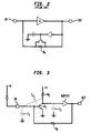
- FIG. 2 One optical preamplifier in the prior art which solves this problem to a degree is shown in Fig. 2.
- the circuit of Fig. 2 was disclosed as Figure 9 in the article entitled "Monolithic GaAs Transimpedance Amplifiers for Fiber-Optic Receivers" by N. Scheinberg et al., pages 1834-1839, IEEE Journal of Solid-State Circuits, Vol. 26, No.12, December 1991.
- AGC automatic control circuit
- the AGC circuit improves the dynamic range of the amplifier and the frequency response remains stable up to an input current as large as 0.5 mA. (milliamperes).
- an optical adaptive transimpedance preamplifier is provided in accordance with the present invention wherein the input of the optical preamplifier is a bipolar junction transistor (BJT) connected in a common emitter stage wherein the collector load resistor has a metal oxide field effect transistor (MOSFET) connected in parallel with the resistor.
- BJT bipolar junction transistor
- MOSFET metal oxide field effect transistor
- the gate of the MOSFET is driven by a voltage whose value is dependent on the output signal level such that the effective collector load impedance is lowered as the output signal level increases in much the same way that the feedback resistor is decreased.
- the collector load impedance is caused to track the feedback impedance in a way such that frequency response stability is maintained with even higher input signal levels.
- the dynamic range is increased even further in accordance with an aspect of the present invention wherein the common emitter amplifier is provided with a second MOSFET connected in parallel with a resistor connected between the emitter of the BJT and ground.
- the voltage provided to the gate of this second MOSFET and the MOSFET type is chosen such that the emitter resistance is completely bypassed by the MOSFET for low signal levels, thereby permitting high amplification, but is permitted to increase in value for increased signal levels.
- the open-loop gain of the preamplifier is decreased for larger signal levels thereby permitting a higher collector resistor and higher sensitivity.
- the maximum input voltage swing is also increased.
- Fig. 2 shows a schematic diagram of a prior art optical transimpedance preamplifier circuit which increases the dynamic range by placing an FET in parallel with the feedback resistor. The gate of the FET is fed by a voltage representing the average value of the output. As the input increases from 0.001 mA. to 0.5 mA., the transimpedance decreases as shown in Fig. 10 of the Scheinberg et al. article.
- Fig. 3 wherein the schematic diagram of a transimpedance type amplifier is shown along with the major parasitic capacitances which affect the frequency response of the amplifier.
- a bipolar junction transistor B1 is connected in a common emitter configuration with its emitter connected to ground and its collector connected both through a collector load resistor R C to a potential source V and to the input of a buffer amplifier.
- the output of the buffer amplifier is connected through a feedback resistor R F to the base electrode of the transistor to form a transimpedance amplifier.
- the dominant pole, p1 which determines the frequency bandwidth of this amplifier can be represented by the following equation: p1 ⁇ a C 1 ⁇ R F where a depicts the open-loop voltage gain of the amplifier, C 1 is the parasitic capacitance associated with the photodetector, base-emitter junction of B1, and the interconnect capacitance. Assuming that the parasitic capacitance C 2 between the base and collector electrodes is negligible, the second pole can be represented by the following equation: p2 ⁇ 1 C 3 ⁇ R C where R C is the collector load resistor, and C 3 is the parasitic capacitance between the collector electrode of B1 and ground including the input capacitance of the buffer amplifier.
- a photodetecting diode 100 is back-biased by a positive potential source 150 connected to its cathode electrode, and the currents developed by the diode by radiation impinging on the diode are coupled from the anode of the diode to an input terminal 101 of the Fig. 1 optical preamplifier.
- the currents from input terminal 101 are coupled to the base electrode of an NPN transistor 102 which is connected as a common emitter stage with its collector electrode connected through a resistor 103 to a positive potential source 150, +V, and its emitter connected through a resistor 104 to ground potential 151.
- a p-channel metal oxide field effect transistor (MOSFET) 105 is connected in parallel with resistor 103 with the source electrode connected to positive potential source 150 and its drain electrode connected to the collector of transistor 102.
- MOSFET metal oxide field effect transistor
- an n-channel MOSFET 106 is connected in parallel with resistor 104 with its source electrode connected to ground potential 151 and its drain electrode connected to the emitter electrode of transistor 102.
- MOSFETs 105 and 106 are connected together and biased in a manner to be described hereinafter with a potential having a value which is dependent on the input signal level. At very low input signal levels, the gates are biased with a potential of about +5 volts causing MOSFET 106 to be completely turned on and to thereby short the emitter of transistor 102 to ground potential. The +5 volts on the gate of MOSFET 105 on the other hand causes it to be completely turned off and the full value of resistor 103 appears as the collector load, R C .
- MOSFET 105 As input signal levels increase, the potential on the gates is decreased causing MOSFET 105 to be turned on and thereby decrease the effective value of the collector load, R C , and causing MOSFET 106 to be driven towards off thereby permitting an effective value of emitter resistance, R E , to be present in the common emitter stage using transistor 102.
- the signal at the collector of transistor 102 is coupled to a buffer amplifier 121 consisting of transistors 107, 109 and 111.
- Transistors 107 and 109 are connected as emitter followers with their respective collectors connected to positive potential source 150 and their emitters connected through resistors 108 and 110 respectively through to ground potential 151.
- the use of the emitter followers advantageously permits the first transistor to be fabricated with a small emitter area such that it does not add significantly to the parasitic capacitance identified hereinabove as C2.
- the second emitter follower with transistor 109 can be fabricated with a larger emitter area in order to increase the amount of power capable of being delivered to the output stage of the buffer amplifier 121 using transistor 111.
- Transistor 111 is connected as a common emitter amplifier stage with its emitter connected through resistor 112 to ground potential and its collector connected through the series combination of resistors 113 and 114 to positive potential source 150.
- Output terminal 140 is connected to the junction of reisistors 113 and 114. In the embodiment which was constructed, the output was taken at this point in order to provide a different dc level than the one which is present at the collector of transistor 111. In should be apparent to those skilled in the art however, that the output could also be taken from the collector of transistor 111 and under these circumstances only one resistor need be present between the collector of transistor 111 and positive potential source 150.
- the signal at the emitter of transistor 111 is coupled through feedback resistor 120 to the base of transistor 102 to provide negative feedback in a standard transimpedance amplifier configuration.
- An n-channel MOSFET 119 is connected in parallel with feedback resistor 120 with its source connected to the emitter of transistor 111 and its drain connected to the base of transistor 102. Accordingly, a potential can be applied to the gate of MOSFET 120 in a manner to be described hereinafter in order to regulate the amount of negative feedback.
- the signal at the collector of transistor 111 is coupled to the input of a noninverting amplifier 115 whose output is connected to an integration circuit consisting of resistor 116 and capacitor 117. Accordingly, bursts of optical energy impinging on photodetecting diode 100 cause the resulting positive pulses on the collector of transistor 111 to be integrated and thereby develop a positive dc potential on capacitor 117.
- the value of positive potential on capacitor 117 is of course dependent on the strength of the optical signal with stronger optical signals causing a larger dc potential.
- the dc potential on capacitor 117 is applied to the gate of n-channel MOSFET 119. As a result, stronger optical signals cause MOSFET to decrease the amount of feedback resistance, R F , thereby decreasing the amplification of the preamplifier to accommodate the stronger optical signals.
- the voltage across capacitor 117 is also coupled to the input of an amplifier 118 whose output is connected to the gates of MOSFETs 105 and 106.
- Amplifier 118 simply inverts the potentials available on capacitor 117. With low optical signal levels and a near zero voltage on capacitor 117, amplifier 118 presents a potential of about +5 volts to the gates of MOSFETs 106 and 107. Under this condition, resistor 104 is completely shorted out and resistor 103 is fully in the circuit resulting in maximum amplification in the preamplifier of Fig. 1.
- the ratio of the poles, p2/p1 can be kept more than 2.75 and stability maintained for even greater decreases in the feedback resistance than in the prior art.
- MOSFET 106 permits the dynamic range to be widened even further. As pointed out hereinabove, for small signal levels MOSFET 106 completely shorts out the emitter resistor 104 and the open loop gain is not affected. In the large signal mode, MOSFET 106 operates in the off mode resulting in the introduction of resistance, R E , in the emitter of transistor 102. The inclusion of MOSFET 106 and resistor 104 serves several purposes. First, in the large signal mode, it reduces the open-loop gain, a, of the preamplifier thereby limiting the increase in the frequency of the first pole, p1, due to the reduction of R F . This in turn allows a higher effective value for R C .
- the choice of component values in the input stage is critical in achieving high sensitivity.
- the principle noise sources are thermal noise due to the feedback resistor, shot noise associated with the base and collector currents of the input transistor, and finally thermal noise contributed by the base resistor. From consideration of the input referred noise, it can be determined that R F and R C must be chosen to be as large as possible while the base resistance of transistor 102 should be minimized. As will be appreciated by those skilled in the art, the relationships set forth hereinabove can be used in order to maximum sensitivity for a given bandwidth. For example, the base resistance can be minimized by making the emitter area of transistor 102 larger. Unfortunately, this will increase the parasitic capacitance C1, and thereby require a decrease in R F in order to keep the pole p1 in the same location.
- the transimpedance begins decreasing at an average input photo current of about 0.01 mA. and continues to decrease up to about 1 mA.
- the embodiment was fabricated in a 1 ⁇ m, 20 GHz BiCMOS technology.
- the frequency bandwidth of about 600 MHz remained well behaved over a broad range of input currents ranging from 1 ⁇ A through to 600 ⁇ A.
- the transimpedance changes by a factor of 25 from small signals to large signals.
Applications Claiming Priority (2)
| Application Number | Priority Date | Filing Date | Title |
|---|---|---|---|
| US360895 | 1994-12-21 | ||
| US08/360,895 US5532471A (en) | 1994-12-21 | 1994-12-21 | Optical transimpedance amplifier with high dynamic range |
Publications (1)
| Publication Number | Publication Date |
|---|---|
| EP0718991A1 true EP0718991A1 (de) | 1996-06-26 |
Family
ID=23419833
Family Applications (1)
| Application Number | Title | Priority Date | Filing Date |
|---|---|---|---|
| EP95308763A Withdrawn EP0718991A1 (de) | 1994-12-21 | 1995-12-05 | Grossignalfester Transimpedanzverstärker für optischen Empfänger |
Country Status (3)
| Country | Link |
|---|---|
| US (1) | US5532471A (de) |
| EP (1) | EP0718991A1 (de) |
| JP (1) | JPH08274546A (de) |
Cited By (6)
| Publication number | Priority date | Publication date | Assignee | Title |
|---|---|---|---|---|
| EP0977353A2 (de) * | 1998-07-29 | 2000-02-02 | Nortel Networks Corporation | Ein Transimpedanzverstärker mit breitem dynamischem Bereich |
| EP1032145A2 (de) * | 1999-02-26 | 2000-08-30 | Nec Corporation | Scaltende optische Empfängerschaltung für Burstbetrieb mit automatischer Verstärkung |
| WO2000052820A1 (en) * | 1999-03-03 | 2000-09-08 | Maxim Integrated Products, Inc. | Transimpedance amplifiers with improved gain-bandwidth product |
| DE102004009684A1 (de) * | 2004-02-27 | 2005-06-09 | Infineon Technologies Ag | Transimpedanzverstärkeranordnung für hohe Schaltfrequenzen |
| US7050724B1 (en) | 1997-11-13 | 2006-05-23 | Nokia Corporation | Optical receiver |
| US8847140B2 (en) | 2012-03-07 | 2014-09-30 | Kabushiki Kaisha Toshiba | Light receiving circuit having an automatic threshold control circuit for forming and allowing electric current flowing between a second potential line and first and second connection points |
Families Citing this family (52)
| Publication number | Priority date | Publication date | Assignee | Title |
|---|---|---|---|---|
| KR0146076B1 (ko) * | 1995-06-28 | 1998-08-01 | 문정환 | 반도체 소자의 기판 전압 레규레이터 장치 |
| US5644418A (en) * | 1995-12-07 | 1997-07-01 | Lucent Technologies Inc. | Smart pixel optical receiver employing sense amplifier and method of operation thereof |
| JP3758750B2 (ja) * | 1996-07-02 | 2006-03-22 | 富士通株式会社 | 光受信装置 |
| US5886570A (en) * | 1997-10-22 | 1999-03-23 | Analog Devices Inc | Inverter circuit biased to limit the maximum drive current to a following stage and method |
| US6084232A (en) * | 1997-11-13 | 2000-07-04 | Matsushita Electric Industrial Co., Ltd. | Optical receiver pre-amplifier which prevents ringing by shunting an input current of the pre-amplifier |
| GB2343943B (en) | 1998-11-18 | 2003-11-26 | Ericsson Telefon Ab L M | Detection circuit |
| US6762644B1 (en) | 2001-03-13 | 2004-07-13 | Marvell International, Ltd. | Apparatus and method for a nested transimpedance amplifier |
| US7551024B2 (en) * | 2001-03-13 | 2009-06-23 | Marvell World Trade Ltd. | Nested transimpedance amplifier |
| US7605649B2 (en) * | 2001-03-13 | 2009-10-20 | Marvell World Trade Ltd. | Nested transimpedance amplifier |
| US7276965B1 (en) | 2001-03-13 | 2007-10-02 | Marvell International Ltd. | Nested transimpedance amplifier |
| US6693492B2 (en) * | 2001-05-18 | 2004-02-17 | International Business Machines Corporation | Variable gain low-noise amplifier and method |
| US6933786B1 (en) * | 2002-05-15 | 2005-08-23 | Cypress Semiconductor Corporation | Amplifier circuit and method |
| US20050061779A1 (en) * | 2003-08-06 | 2005-03-24 | Walter Blumenfeld | Laser ablation feedback spectroscopy |
| US20050046482A1 (en) * | 2003-08-27 | 2005-03-03 | Karl Schrodinger | Receiver circuit |
| KR100515078B1 (ko) * | 2003-09-03 | 2005-09-14 | 삼성전기주식회사 | 전류 검출에 의한 리미터 회로를 채용한 전류-전압 변환및 증폭 회로 |
| KR100617294B1 (ko) * | 2003-11-24 | 2006-08-30 | 한국전자통신연구원 | 자동 이득 조절 귀환 증폭기 |
| US7239202B1 (en) | 2004-03-31 | 2007-07-03 | Marvell International Ltd. | Variable-gain constant-bandwidth transimpedance amplifier |
| US7023271B1 (en) | 2004-03-31 | 2006-04-04 | Marvell International Ltd. | Variable-gain constant-bandwidth transimpedance amplifier |
| US7558014B1 (en) | 2004-06-24 | 2009-07-07 | Marvell International Ltd. | Programmable high pass amplifier for perpendicular recording systems |
| US7385170B1 (en) | 2004-08-24 | 2008-06-10 | Semiconductor Components Industries, Llc | Ambient light suppression circuit for photodiode receiver applications |
| JP4244913B2 (ja) * | 2004-11-18 | 2009-03-25 | パナソニック株式会社 | 受光増幅回路 |
| DE102004060076A1 (de) * | 2004-12-14 | 2006-07-06 | Merck Patent Gmbh | Verfahren zur Herstellung von Onium-Salzen mit Alkyl- oder Arylsulfonat-Anionen oder Alkyl- oder Arylcarboxylat-Anionen mit geringem Halogenid-Gehalt |
| US7518447B1 (en) | 2005-01-18 | 2009-04-14 | Marvell International Ltd. | Transimpedance amplifier |
| US7449958B1 (en) | 2005-08-17 | 2008-11-11 | Marvell International Ltd. | Open loop DC control for a transimpedance feedback amplifier |
| JP4566893B2 (ja) * | 2005-11-25 | 2010-10-20 | シャープ株式会社 | 受光増幅回路、及び、光ピックアップ装置 |
| US7659776B2 (en) * | 2006-10-17 | 2010-02-09 | Cypress Semiconductor Corporation | Offset voltage correction for high gain amplifier |
| JP2009100337A (ja) * | 2007-10-18 | 2009-05-07 | Renesas Technology Corp | 可変利得増幅器を内蔵する半導体集積回路 |
| US7605660B1 (en) | 2007-11-12 | 2009-10-20 | Rf Micro Devices, Inc. | Linear multi-stage transimpedance amplifier |
| US7948323B2 (en) * | 2009-05-06 | 2011-05-24 | Mindspeed Technologies, Inc. | Linear transimpedance amplifier with wide dynamic range for high rate applications |
| JP5161189B2 (ja) * | 2009-10-23 | 2013-03-13 | 日本電信電話株式会社 | トランスインピーダンスアンプ |
| JP5459258B2 (ja) * | 2011-04-15 | 2014-04-02 | Tdk株式会社 | 並列−直列形電流帰還増幅器、増幅器、及び光学機器 |
| US9107245B2 (en) | 2011-06-09 | 2015-08-11 | Mindspeed Technologies, Inc. | High accuracy, high dynamic range LED/laser driver |
| US9059065B2 (en) * | 2012-03-19 | 2015-06-16 | National Institute Of Advanced Industrial Science And Technology | Method of varying gain of amplifying photoelectric conversion device and variable gain photoelectric conversion device |
| US9385606B2 (en) | 2012-12-03 | 2016-07-05 | M/A-Com Technology Solutions Holdings, Inc. | Automatic buck/boost mode selection system for DC-DC converter |
| KR101513373B1 (ko) * | 2013-12-31 | 2015-04-20 | 한양대학교 산학협력단 | 직류 오프셋을 보상하는 광통신 수신기 |
| US10097908B2 (en) | 2014-12-31 | 2018-10-09 | Macom Technology Solutions Holdings, Inc. | DC-coupled laser driver with AC-coupled termination element |
| US10044328B2 (en) | 2015-07-20 | 2018-08-07 | Macom Technology Solutions Holdings, Inc. | Transimpedance amplifier with bandwidth extender |
| WO2017023240A1 (en) * | 2015-07-31 | 2017-02-09 | Hewlett Packard Enterprise Development Lp | Optical receivers |
| US10333628B2 (en) | 2016-06-10 | 2019-06-25 | Hewlett Packard Enterprise Development Lp | Optical receivers |
| US10263573B2 (en) | 2016-08-30 | 2019-04-16 | Macom Technology Solutions Holdings, Inc. | Driver with distributed architecture |
| JP6812263B2 (ja) | 2017-02-10 | 2021-01-13 | オムロン株式会社 | 光電センサおよび投光器 |
| US10338224B2 (en) | 2017-03-27 | 2019-07-02 | Analog Devices Global Unlimited Company | High dynamic range analog front-end receiver for long range LIDAR |
| US10686412B2 (en) | 2017-03-29 | 2020-06-16 | Linear Technology Corporation | Trans-impedance amplifier with fast overdrive recovery |
| US10630052B2 (en) | 2017-10-04 | 2020-04-21 | Macom Technology Solutions Holdings, Inc. | Efficiency improved driver for laser diode in optical communication |
| US10505509B2 (en) | 2017-10-31 | 2019-12-10 | Cisco Technology, Inc. | Process and temperature insensitive linear circuit |
| US11018637B2 (en) * | 2018-02-14 | 2021-05-25 | Analog Devices Global Unlimited Company | High dynamic range transimpedance amplifier |
| WO2019208122A1 (ja) | 2018-04-27 | 2019-10-31 | パナソニックIpマネジメント株式会社 | 増幅回路 |
| US11555897B2 (en) | 2018-07-02 | 2023-01-17 | Analog Devices International Unlimited Company | Transimpedance amplifier with pulse widening |
| US11005573B2 (en) | 2018-11-20 | 2021-05-11 | Macom Technology Solutions Holdings, Inc. | Optic signal receiver with dynamic control |
| US11249499B2 (en) | 2020-03-04 | 2022-02-15 | Cisco Technology, Inc. | Linear transimpedance amplifier dual regulator architecture and tuning |
| US11658630B2 (en) | 2020-12-04 | 2023-05-23 | Macom Technology Solutions Holdings, Inc. | Single servo loop controlling an automatic gain control and current sourcing mechanism |
| CN113659943B (zh) * | 2021-07-30 | 2023-08-01 | 江苏科大亨芯半导体技术有限公司 | 大动态范围跨阻放大器 |
Citations (2)
| Publication number | Priority date | Publication date | Assignee | Title |
|---|---|---|---|---|
| DE3204839A1 (de) * | 1982-02-11 | 1983-09-01 | Siemens AG, 1000 Berlin und 8000 München | Fotodiodenverstaerker mit grossem dynamikbereich |
| DE4212934A1 (de) * | 1992-04-18 | 1993-10-21 | Sel Alcatel Ag | Schaltungsanordnung für einen optischen Empfänger |
Family Cites Families (7)
| Publication number | Priority date | Publication date | Assignee | Title |
|---|---|---|---|---|
| US4540952A (en) * | 1981-09-08 | 1985-09-10 | At&T Bell Laboratories | Nonintegrating receiver |
| DE3336366C2 (de) * | 1983-10-06 | 1985-08-14 | Telefunken electronic GmbH, 7100 Heilbronn | Breitbandverstärker zur Verstärkung eines Fotostromes |
| US4564818A (en) * | 1984-08-24 | 1986-01-14 | Motorola Inc. | Transimpedance amplifier having an improved gain/bandwidth product |
| US4792998A (en) * | 1986-05-23 | 1988-12-20 | Siemens Aktiengesellschaft | Receiver for optical digital signals having different amplitudes |
| DE3806283A1 (de) * | 1988-02-27 | 1989-09-07 | Telefunken Electronic Gmbh | Optoelektronischer transimpedanz-verstaerker |
| DE4212933A1 (de) * | 1992-04-18 | 1993-10-21 | Sel Alcatel Ag | Schaltungsanordnung für einen optischen Empfänger |
| JPH05304422A (ja) * | 1992-04-24 | 1993-11-16 | Sumitomo Electric Ind Ltd | 光通信用前置増幅器 |
-
1994
- 1994-12-21 US US08/360,895 patent/US5532471A/en not_active Expired - Lifetime
-
1995
- 1995-12-05 EP EP95308763A patent/EP0718991A1/de not_active Withdrawn
- 1995-12-20 JP JP7331275A patent/JPH08274546A/ja not_active Withdrawn
Patent Citations (2)
| Publication number | Priority date | Publication date | Assignee | Title |
|---|---|---|---|---|
| DE3204839A1 (de) * | 1982-02-11 | 1983-09-01 | Siemens AG, 1000 Berlin und 8000 München | Fotodiodenverstaerker mit grossem dynamikbereich |
| DE4212934A1 (de) * | 1992-04-18 | 1993-10-21 | Sel Alcatel Ag | Schaltungsanordnung für einen optischen Empfänger |
Non-Patent Citations (2)
| Title |
|---|
| MIKAMURA ET AL: "GaAs IC chip set of compact optical module of Giga bit rates", INTERNATIONAL CONFERENCE ON INDUSTRIAL ELECTRONICS, CONTROL AND INSTRUMENTATION (IECON '91), 28 October 1991 (1991-10-28) - 1 November 1991 (1991-11-01), KOBE, JP, pages 2574 - 2579, XP000325599 * |
| WILLIAMS: "La contre-réaction en courant s'impose à frequence élevée", ELECTRONIQUE, no. 19, PARIS FR, pages 68 - 72, XP000304872 * |
Cited By (9)
| Publication number | Priority date | Publication date | Assignee | Title |
|---|---|---|---|---|
| US7050724B1 (en) | 1997-11-13 | 2006-05-23 | Nokia Corporation | Optical receiver |
| EP0977353A2 (de) * | 1998-07-29 | 2000-02-02 | Nortel Networks Corporation | Ein Transimpedanzverstärker mit breitem dynamischem Bereich |
| EP0977353A3 (de) * | 1998-07-29 | 2002-03-20 | Nortel Networks Limited | Ein Transimpedanzverstärker mit breitem dynamischem Bereich |
| EP1032145A2 (de) * | 1999-02-26 | 2000-08-30 | Nec Corporation | Scaltende optische Empfängerschaltung für Burstbetrieb mit automatischer Verstärkung |
| EP1032145A3 (de) * | 1999-02-26 | 2002-04-10 | Nec Corporation | Scaltende optische Empfängerschaltung für Burstbetrieb mit automatischer Verstärkung |
| WO2000052820A1 (en) * | 1999-03-03 | 2000-09-08 | Maxim Integrated Products, Inc. | Transimpedance amplifiers with improved gain-bandwidth product |
| DE102004009684A1 (de) * | 2004-02-27 | 2005-06-09 | Infineon Technologies Ag | Transimpedanzverstärkeranordnung für hohe Schaltfrequenzen |
| DE102004009684B4 (de) * | 2004-02-27 | 2014-12-24 | Infineon Technologies Ag | Transimpedanzverstärkeranordnung für hohe Schaltfrequenzen |
| US8847140B2 (en) | 2012-03-07 | 2014-09-30 | Kabushiki Kaisha Toshiba | Light receiving circuit having an automatic threshold control circuit for forming and allowing electric current flowing between a second potential line and first and second connection points |
Also Published As
| Publication number | Publication date |
|---|---|
| JPH08274546A (ja) | 1996-10-18 |
| US5532471A (en) | 1996-07-02 |
Similar Documents
| Publication | Publication Date | Title |
|---|---|---|
| US5532471A (en) | Optical transimpedance amplifier with high dynamic range | |
| JP3158759B2 (ja) | 同相モード安定性が強化された差動増幅器 | |
| US6583671B2 (en) | Stable AGC transimpedance amplifier with expanded dynamic range | |
| EP0181146B1 (de) | Transimpedanzverstärker | |
| US5442321A (en) | Automatic transimpedance control amplifier | |
| US4764732A (en) | Switchable mode amplifier for wide dynamic range | |
| US5030925A (en) | Transimpedance amplifier | |
| US5734300A (en) | Optical receiver preamplifier dynamic range enhancing circuit and method | |
| US5525929A (en) | Transimpedance amplifier circuit with feedback and load resistor variable circuits | |
| US4901031A (en) | Common-base, source-driven differential amplifier | |
| US4563656A (en) | Wideband transimpedance optical receiver | |
| US4075576A (en) | Sensitive high speed solid state preamp | |
| US6323734B1 (en) | Trans-impedance amplifier | |
| KR950000162B1 (ko) | 증폭기 장치 및 푸시풀 증폭기 | |
| US4553108A (en) | Low noise feedback amplifier | |
| US4433303A (en) | Push-pull amplifier circuit with field-effect transistors | |
| US5939944A (en) | NPN push-pull output stage with folded cascode JFETs | |
| US4507615A (en) | Non-linear amplifier systems | |
| US5045808A (en) | Single-stage high-gain amplifier | |
| US4194166A (en) | Differential amplifier with a current mirror circuit | |
| US5406222A (en) | High gain transistor amplifier | |
| EP0354557B1 (de) | Differenzverstärker mit verbesserter Verstärkungscharakteristik in einem Hochfrequenzbereich | |
| US4241314A (en) | Transistor amplifier circuits | |
| US4142110A (en) | Circuit to eliminate DC bias | |
| EP1014567B1 (de) | Verbesserungen an oder in Bezug auf einen Operationsverstärker |
Legal Events
| Date | Code | Title | Description |
|---|---|---|---|
| PUAI | Public reference made under article 153(3) epc to a published international application that has entered the european phase |
Free format text: ORIGINAL CODE: 0009012 |
|
| AK | Designated contracting states |
Kind code of ref document: A1 Designated state(s): DE ES FR GB |
|
| 17P | Request for examination filed |
Effective date: 19961205 |
|
| STAA | Information on the status of an ep patent application or granted ep patent |
Free format text: STATUS: THE APPLICATION HAS BEEN WITHDRAWN |
|
| 18W | Application withdrawn |
Withdrawal date: 19971006 |