EP0713293A2 - Rücksetzgeneratorschaltung zum Rücksetzen von sich selbst rücksetzenden CMOS-Schaltungen - Google Patents
Rücksetzgeneratorschaltung zum Rücksetzen von sich selbst rücksetzenden CMOS-Schaltungen Download PDFInfo
- Publication number
- EP0713293A2 EP0713293A2 EP95480138A EP95480138A EP0713293A2 EP 0713293 A2 EP0713293 A2 EP 0713293A2 EP 95480138 A EP95480138 A EP 95480138A EP 95480138 A EP95480138 A EP 95480138A EP 0713293 A2 EP0713293 A2 EP 0713293A2
- Authority
- EP
- European Patent Office
- Prior art keywords
- node
- circuit
- reset
- gate
- fet
- Prior art date
- Legal status (The legal status is an assumption and is not a legal conclusion. Google has not performed a legal analysis and makes no representation as to the accuracy of the status listed.)
- Withdrawn
Links
- 230000003111 delayed effect Effects 0.000 claims 1
- 238000007599 discharging Methods 0.000 claims 1
- 230000008030 elimination Effects 0.000 claims 1
- 238000003379 elimination reaction Methods 0.000 claims 1
- 230000005669 field effect Effects 0.000 claims 1
- 230000010355 oscillation Effects 0.000 abstract description 4
- 230000000295 complement effect Effects 0.000 description 8
- 238000010586 diagram Methods 0.000 description 6
- 230000001934 delay Effects 0.000 description 3
- 238000004088 simulation Methods 0.000 description 2
- 230000007704 transition Effects 0.000 description 2
- 229910044991 metal oxide Inorganic materials 0.000 description 1
- 150000004706 metal oxides Chemical class 0.000 description 1
- 230000004048 modification Effects 0.000 description 1
- 238000012986 modification Methods 0.000 description 1
- 239000004065 semiconductor Substances 0.000 description 1
Images


Classifications
-
- H—ELECTRICITY
- H03—ELECTRONIC CIRCUITRY
- H03K—PULSE TECHNIQUE
- H03K3/00—Circuits for generating electric pulses; Monostable, bistable or multistable circuits
- H03K3/02—Generators characterised by the type of circuit or by the means used for producing pulses
- H03K3/353—Generators characterised by the type of circuit or by the means used for producing pulses by the use, as active elements, of field-effect transistors with internal or external positive feedback
- H03K3/356—Bistable circuits
- H03K3/356008—Bistable circuits ensuring a predetermined initial state when the supply voltage has been applied; storing the actual state when the supply voltage fails
Definitions
- the present invention generally relates to self-resetting complementary metal oxide semiconductor (CMOS) circuits manufactured as integrated circuit(IC) chips and, more specifically, to a reset generating circuit to reset the self-resetting CMOS (SRCMOS) circuits during regular and long clock cycles.
- CMOS complementary metal oxide semiconductor
- the basic concept of an SRCMOS circuit is to provide a high speed timed data path.
- a RESET signal makes a transition from high to low. This will charge a node of the circuit to the supply voltage.
- the RESET pulse is approximately 700 picoseconds wide.
- a data signal on an input terminal will go from low to high. This action will discharge the precharged node to ground, causing the output signal at an output terminal to go high.
- the RESET signal will pulse.
- the RESET generation circuit for the SRCMOS circuit creates two problems. First, under certain conditions, the RESET signal will oscillate. Second, a very wide clock pulse width used in the circuit can cause a collision current phenomena.
- an SRCMOS circuit that works with a variable clock cycle. More specifically, the circuit operates in either a long or short clock cycle. Circuit oscillation is avoided in either long or short clock cycles. At the same time, the circuit eliminates overlapping currents by incorporating a ground interrupt device. The reset generation path is optimized to provide a fast and narrow reset pulse. A reset pulse is selectively generated only in cycles that require it. In addition, the circuit saves power.
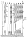
- the basic SRCMOS circuit shown in Figure 1, comprises an n-channel FET 11 and p-channel FET 12.
- the sources of FETs 12 and 11 are connected to VDD and ground, respectively.
- the gate of FET 12 is connected to the RESET input terminal, and the gate of FET 11 is connected to a second input terminal IN0.
- the common node between the drains of FETs 11 and 12 is connected to node 13.
- Node 13 is also connected to the common drain connection of a second pair of FETs comprising n-channel FET 14 and p-channel FET 15.
- the source of FET 15 is connected to V DD , and the drain of FET 15 is connected to node 13. Similarly, the source of FET 14 is connected to ground, and the drain is connected to node 13.
- the node 13 is also connected to an invertor 16, the output of which is connected to the OUTPUT terminal.
- the signal at the output of invertor 16 is also connected to the gates of FETs 14 and 15.
- the combination of the FETs 14 and 15 and invertor 16 form a latch which, in operation, must first be reset by precharging node 13 to V DD .
- FIG. 2 An example of RESET generation is shown in Figure 2.
- the input clock signal CLKG is fed to an invertor 21 having its output connected to the gate of n-channel FET 22.
- the source of FET 22 is connected to ground, and the drain of FET 22 is connected to node 23.
- the sources of p-channel FETs 24 and 25 are connected to node 23.
- Node 23 is also the input for the invertor 26.
- the output of inventor 26 is node 27.
- Node 27 is fed to one input of NAND gate 28 and also to the gate of FET 25.
- the other input to NAND gate 28 is node 29, the output of invertor 30 which receives as its input the EVALOUT signal via invertor string 31 and 32.
- the output of NAND gate 28 is the RESET signal.
- This RESET signal becomes the input to invertor 33 and p-channel FET 12, shown in Figure 1.
- Invertor 33 is part of the invertor string which comprises invertors 34 and 35, the output of which is node 36.
- Node 36 is one of the inputs to NAND gate 37, and the other input is node 38, the output of invertor 39 which receives as its input the P_RESET signal.
- the output of NAND gate 37 is node 40 which is connected to the gate of p-channel FET 24.
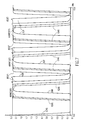
- the clock signal CLKG will go from high to low.
- CLKG goes low
- the output of invertor 21 is forced high and n-channel FET 22 begins to conduct. This action discharges node 23 to ground, causing node 27 to go high due to the action of invertor 26.
- the signals EVALOUT and P_RESET are low and therefore nodes 29 and 38 will be high, respectively due to the actions of invertor string 30 to 32 and invertor 39.
- node 27 goes high, the RESET signal is pulled low.
- node 36 is forced high due to the action of invertor string 33 to 35, causing node 40 to go low.
- the cycle time of the clock signal CLKG is 2.5 nanoseconds (ns) and if the clock signal CLKG is assumed to have a 50% duty cycle, then the clock signal CLKG will stay low for about 1.25 ns.
- Figure 4 is the reset generating circuit
- Figure 5 is a portion of a SRCMOS circuit used to detect the arrival of an address for an array.
- the AIN signal is a signal that selected the RESET generation circuit in order to provide a RESET signal to reset the SRCMOS circuits in the following cycle. If no AIN signal is asserted, there will be no RESET generated in the next cycle. The output of this circuit is the RESET signal.
- the RESET signal resets the SRCMOS circuit shown in Figure 5.
- Input AIN is fed top one input of NAND gate 41.
- the second input of NAND gate 41 is supplied by the output of NAND gate 42.
- the clock signal CLKG is input to two invertors 43 and 44.
- the output of the invertor 43 is one of the inputs of NAND gate 42.
- the output of NAND gate 41 at node 45 is connected to one input of NOR gate 46, the second input of which is connected to node 48.
- the output of NOR gate 46 is connected to the gate of n-channel FET 49, and the output of invertor 44 is connected to the gate of n-channel FET 50.
- the FETs 49 and 50 are connected in series between node 51 and ground. Thus, when the outputs of the NOR gate 46 and invertor 44 are both high, the FETs 49 and 50 discharge node 51 to ground.
- Node 51 is also connected to the drains of p-channel FETs 52 and 53 and to the drains of n-channel FETs 54 and 55.
- the input of invertor 56 is node 51 and the output is node 57, which is connected to the gates of p-channel FET 53 and n-channel FET 55.
- the gate of FET 52 is connected to node 58, and the source of FET 52 is connected to V DD .
- invertor 56 is also connected to invertor 59 which, in turn, is connected to the RESET output terminal.
- a delay chain of two invertors 60 and 61 is connected between P_RESET and node 62.
- the output of invertor 61 drives invertor 63 whose output is connected to the gate of n-channel FET 54, and the output of invertor 61, node 62, is one of the inputs of NOR gate 64.
- the second input of the NOR gate 64 is the RESET signal, and the output NOR gate 64 is node 48.
- Node 48 is the second input to NOR gate 46 and is also connected to the input of invertor 65, the output of which is connected, via invertor string 66 and 67, to one input of NAND gate 68 and directly to the other input of NAND gate 68.
- the output of NAND gate 68 is connected to the invertor 69 whose output is connected to the gate of p-channel FET 52.
- the second input of NAND gate 42 is supplied by the output of inverter 43 via inverter string 70 to 73 to establish a time delay.
- Figure 5 depicts a circuit to detect the arrival of address bits A3 to A9.
- the true and complement address bits are both low when no address is present. When an address is present, either the true or the complement address bit will be high.
- A3 to A9 are the "true” and A3 ⁇ to A9 ⁇ are the "complement of the signal.
- the true addresses from A3 to A9 and complement addresses from A3 ⁇ to A9 ⁇ are respectively ORed and the results are then ANDed together to generate the output signal at the OUT terminal.
- the output signal is connected to AIN in Figure 4.
- the RESET signal from Figure 4 is connected to the gates of p-channel FETs 75, 76 and 77.
- the sources of the FETs 75, 76 and 77 are connected to V DD , and their drains are connected to nodes 78, 79 and 80, respectively.
- the address bit A3 is connected to the gate of n-channel FET 81, and its complement, address bit A3, is connected to the gate of n-channel FET 82. Both FETs 81 and 82 have a common drain connection to node 78 and common source connection to node 83.
- address bit A4 is connected to the gate of n-channel FET 84, and its complement, address bit A4, is connected to n-channel FET 85.
- FETs 84 and 85 have common source connection to node 86 and a common drain connection to node 83.
- Address bits A5 and A5 are respectively input to the gates of n-channel FETs 87 and 88, which have a common drain connection to node 86.
- the sources of FETs 87 and 88 are connected to ground.
- Node 78 is also connected to the input of invertor 89 and to the drains of p-channel FET 90 and n-channel FET 91.
- the source of FET 90 is connected to VDD, and the source of FET 91 is connected to ground.
- the output of invertor 89 is connected to the gates of FETs 90 and 91 and also to one input of NAND gate 92.
- NAND 92 The three inputs of NAND 92 are nodes 93, 94 and 95, and its output is node 96 which is connected to the input of invertor 97.
- the output of invertor 97 is the output terminal OUT which is connected to input terminal AIN in Figure 4.
- the P_RESET signal in Figure 4 is high which forces the output of invertors 63 and 61 to be high. This action forces node 51 and the RESET signal to be low. If the RESET signal is low, all SRCMOS circuits in Figure 5 are reset; i.e., all the SRCMOS circuits are precharged to V DD . For example, nodes 78, 79 and 90 are precharged to V DD in Figure 5, and the output signal at the OUT terminal is forced low. Also, node 62 is high which forces node 58 to go high, keeping p-channel FET 52 off. Once the P_RESET signal goes low, this will allow the circuit in Figure 4 to reset itself; i.e., node 51 is precharged to V DD .
- Input AIN is generated by combining all the row addresses A3 to A9 as shown in Figure 5.
- the cycle begins with the clock signal CLKG going from high to low.
- the clock signal CLKG goes low, approximately 1.5 ns later, all the input addresses will go high; i.e., either true or complement addresses A3 to A9 will switch high in one cycle.
- the high going address inputs A3 to A9 will pull nodes 78, 79 and 80 to ground. Consequently, nodes 93, 94 and 95 are pulled high.
- the output of NAND gate 92 is forced low and the output of invertor 97 is forced high.
- the first key feature of this circuit is that the latest address sets this circuit; i.e., the output signal on the OUT terminal is forced high. This means that if the addresses are coming from a long distance, the circuit will wait for the last address to come before switching. This eliminates any false RESET generation.
- the second key feature is that once the AIN input signal makes a positive transition, it will not reset until the RESET signal goes low. This will cause the AIN input signal to remain high regardless of the cycle time.
- the clock signal CLKG going negative starts the cycle.
- the first path causes the output of invertor 44 in Figure 4 to go low, interrupting ground and preventing the positive going output of NOR gate 46 from pulling node 51 low until the next cycle.
- the second path will cause high going output of NAND gate 42 to be able to pass through the NAND gate 41 if input signal AIN is high. Since there are four gate delays in the second path to the output of NOR gate 46 when the clock signal CLKG goes high versus only one gate delay for the first path, the output of invertor 44 will always turn off before the output of NOR gate 46 goes high.
- the third path is a longer path than the second path and has eight stages, including the invertor chain 70 to 73.
- This path is designed so that it takes a long time for the falling edge of clock signal CLKG to cause the output of NOR gate 46 to go low, while the first path is very fast with only one stage. This will guarantee that outputs of NOR gate 46 and invertor 44 will both be high at the beginning of the cycle if the input signal AIN is pulsed high in the previous cycle, and thus starting a reset in cycle 2.
- the clock signal CLKG works in two modes; a regular mode and a long cycle mode.
- the cycle time of the clock signal CLKG is 2.7 ns. If it is assumed that the clock signal CLKG has a duty cycle of 50%, then the clock signal CLKG will stay either low or high for 1.35 ns.
- the clock signal CLKG In the long cycle mode, the clock signal CLKG either stays low or high for a long time. When the clock signal CLKG goes low, after a certain time delay, all the addresses go high (approximately 1.5 ns later). This forces the output signal on the OUT terminal in Figure 5 to go high.
- the output of NAND gate 42 in Figure 4 is already low, and node 44 is high. This keeps the output of NOR gate node 46 low. Although the output of invertor 44 is high, the output of NOR gate 46 is low and keeps node 51 precharged to V DD .
Landscapes
- Electronic Switches (AREA)
- Static Random-Access Memory (AREA)
- Logic Circuits (AREA)
Applications Claiming Priority (2)
| Application Number | Priority Date | Filing Date | Title |
|---|---|---|---|
| US342967 | 1994-11-21 | ||
| US08/342,967 US5467037A (en) | 1994-11-21 | 1994-11-21 | Reset generation circuit to reset self resetting CMOS circuits |
Publications (2)
| Publication Number | Publication Date |
|---|---|
| EP0713293A2 true EP0713293A2 (de) | 1996-05-22 |
| EP0713293A3 EP0713293A3 (de) | 1998-07-22 |
Family
ID=23344083
Family Applications (1)
| Application Number | Title | Priority Date | Filing Date |
|---|---|---|---|
| EP95480138A Withdrawn EP0713293A3 (de) | 1994-11-21 | 1995-09-22 | Rücksetzgeneratorschaltung zum Rücksetzen von sich selbst rücksetzenden CMOS-Schaltungen |
Country Status (3)
| Country | Link |
|---|---|
| US (1) | US5467037A (de) |
| EP (1) | EP0713293A3 (de) |
| TW (1) | TW273044B (de) |
Cited By (1)
| Publication number | Priority date | Publication date | Assignee | Title |
|---|---|---|---|---|
| US5455045A (en) * | 1993-05-13 | 1995-10-03 | Syntex (U.S.A.) Inc. | High dose formulations |
Families Citing this family (19)
| Publication number | Priority date | Publication date | Assignee | Title |
|---|---|---|---|---|
| JP3299032B2 (ja) * | 1994-05-17 | 2002-07-08 | 松下電器産業株式会社 | 初期値設定回路 |
| US5617047A (en) * | 1995-06-06 | 1997-04-01 | International Business Machines Corporation | Reset and pulse width control circuits for high-performance multi-port memories and register files |
| US5686847A (en) * | 1996-03-15 | 1997-11-11 | Rockwell International Corporation | Reduced sensitivity power-on reset circuitry |
| US5646566A (en) * | 1996-06-21 | 1997-07-08 | International Business Machines Corporation | Low power clocked set/reset fast dynamic latch |
| US5952861A (en) * | 1997-06-19 | 1999-09-14 | Sun Microsystems, Inc. | Dynamic pulse register with scan functionality |
| US5973531A (en) * | 1997-06-20 | 1999-10-26 | Sun Microsystems, Inc. | Method for generating a pulse output in a dynamic register |
| KR100272672B1 (ko) | 1997-12-31 | 2000-11-15 | 윤종용 | 다이나믹 씨모오스 회로 |
| US6085327A (en) * | 1998-04-10 | 2000-07-04 | Tritech Microelectronics, Ltd. | Area-efficient integrated self-timing power start-up reset circuit with delay of the start-up reset until the system clock is stabilized |
| US6084454A (en) * | 1998-08-26 | 2000-07-04 | Advanced Micro Devices, Inc. | Start-up circuit for write selects and equilibrates |
| US6232798B1 (en) * | 1999-12-09 | 2001-05-15 | International Business Machines Corporation | Self-resetting circuit timing correction |
| US6973420B1 (en) * | 2000-06-30 | 2005-12-06 | Intel Corporation | Digital circuit simulation |
| US6567337B1 (en) | 2000-06-30 | 2003-05-20 | Intel Corporation | Pulsed circuit topology to perform a memory array write operation |
| US6531897B1 (en) | 2000-06-30 | 2003-03-11 | Intel Corporation | Global clock self-timed circuit with self-terminating precharge for high frequency applications |
| US6496038B1 (en) | 2000-06-30 | 2002-12-17 | Intel Corporation | Pulsed circuit topology including a pulsed, domino flip-flop |
| US6542006B1 (en) * | 2000-06-30 | 2003-04-01 | Intel Corporation | Reset first latching mechanism for pulsed circuit topologies |
| US6549039B1 (en) * | 2000-09-27 | 2003-04-15 | Intel Corporation | Hi gain clock circuit |
| US6628139B2 (en) | 2001-08-03 | 2003-09-30 | Micron Technology, Inc. | Digital logic devices with extremely skewed trip points and reset circuitry for rapidly propagating signal edges |
| US7429884B2 (en) * | 2005-11-18 | 2008-09-30 | Sun Microsystems, Inc. | Pulse-signaling circuits for networks on chip |
| US8179171B1 (en) * | 2008-03-27 | 2012-05-15 | Synopsys Inc. | Power up circuit |
Family Cites Families (14)
| Publication number | Priority date | Publication date | Assignee | Title |
|---|---|---|---|---|
| US4164666A (en) * | 1976-06-08 | 1979-08-14 | Toyko Shibaura Electric Co., Ltd. | Electronic apparatus using complementary MOS transistor dynamic clocked logic circuits |
| US4423338A (en) * | 1982-03-01 | 1983-12-27 | International Business Machines Corporation | Single shot multivibrator having reduced recovery time |
| US4583008A (en) * | 1983-02-25 | 1986-04-15 | Harris Corporation | Retriggerable edge detector for edge-actuated internally clocked parts |
| US4806794A (en) * | 1987-07-22 | 1989-02-21 | Advanced Micro Devices, Inc. | Fast, low-noise CMOS output buffer |
| JPH01144719A (ja) * | 1987-11-30 | 1989-06-07 | Toshiba Corp | リトリガブル・マルチバイブレータ |
| US5015881A (en) * | 1990-03-02 | 1991-05-14 | International Business Machines Corp. | High speed decoding circuit with improved AND gate |
| US5061864A (en) * | 1990-06-18 | 1991-10-29 | National Semiconductor Corporation | Monophase logic |
| JP3088821B2 (ja) * | 1992-03-18 | 2000-09-18 | 沖電気工業株式会社 | パワーオンリセット回路 |
| JP3023238B2 (ja) * | 1992-04-09 | 2000-03-21 | 株式会社東芝 | パワ−オンリセットシステムおよびこのパワ−オンリセットシステムを具備する半導体記憶装置 |
| US5323066A (en) * | 1992-06-01 | 1994-06-21 | Motorola, Inc. | Method and apparatus for performing power on reset initialization in a data processing system |
| US5331224A (en) * | 1992-08-19 | 1994-07-19 | National Semiconductor Corporation | Icct leakage current interrupter |
| US5298799A (en) * | 1992-12-31 | 1994-03-29 | International Business Machines Corporation | Single-shot circuit with fast reset |
| US5323067A (en) * | 1993-04-14 | 1994-06-21 | National Semiconductor Corporation | Self-disabling power-up detection circuit |
| US5371772A (en) * | 1993-09-14 | 1994-12-06 | Intel Corporation | Programmable divider exhibiting a 50/50 duty cycle |
-
1994
- 1994-11-21 US US08/342,967 patent/US5467037A/en not_active Expired - Fee Related
-
1995
- 1995-08-10 TW TW084108333A patent/TW273044B/zh active
- 1995-09-22 EP EP95480138A patent/EP0713293A3/de not_active Withdrawn
Non-Patent Citations (1)
| Title |
|---|
| None |
Cited By (1)
| Publication number | Priority date | Publication date | Assignee | Title |
|---|---|---|---|---|
| US5455045A (en) * | 1993-05-13 | 1995-10-03 | Syntex (U.S.A.) Inc. | High dose formulations |
Also Published As
| Publication number | Publication date |
|---|---|
| TW273044B (en) | 1996-03-21 |
| US5467037A (en) | 1995-11-14 |
| EP0713293A3 (de) | 1998-07-22 |
Similar Documents
| Publication | Publication Date | Title |
|---|---|---|
| US5467037A (en) | Reset generation circuit to reset self resetting CMOS circuits | |
| US5115150A (en) | Low power CMOS bus receiver with small setup time | |
| US6111447A (en) | Timing circuit that selectively triggers on a rising or falling input signal edge | |
| US5221867A (en) | Programmable logic array with internally generated precharge and evaluation timing | |
| US5812462A (en) | Integrated circuit clock input buffer | |
| KR100254317B1 (ko) | 동작주기적응형데이터출력버퍼 | |
| US5949721A (en) | Data output related circuit which is suitable for semiconductor memory device for high -speed operation | |
| KR920020842A (ko) | 고속 패스게이트, 래치 및 플립-플롭 회로 | |
| EP0574606B1 (de) | Pulsformerschaltung mit ausgewählter Verzögerung des Pulsanstiegs | |
| US6204714B1 (en) | Variable width pulse generator | |
| EP1087529B1 (de) | Halteschaltung in Dominologic mit Rückstellzeit | |
| US6486713B2 (en) | Differential input buffer with auxiliary bias pulser circuit | |
| US6646474B2 (en) | Clocked pass transistor and complementary pass transistor logic circuits | |
| JP2805466B2 (ja) | メモリのアドレス遷移検出回路 | |
| US6239621B1 (en) | Two legged reset controller for domino circuit | |
| US6275069B1 (en) | Self-resetting logic circuits and method of operation thereof | |
| US4129793A (en) | High speed true/complement driver | |
| GB2092850A (en) | Pulse generating circuit | |
| US6407608B1 (en) | Clock input buffer with increased noise immunity | |
| KR100233331B1 (ko) | 신호천이검출회로 | |
| US7173456B2 (en) | Dynamic logic return-to-zero latching mechanism | |
| KR19980050806A (ko) | 비동기적으로 프리차지 및 활성화 되는 메모리의 기준 클럭 발생회로 | |
| US5864251A (en) | Method and apparatus for self-resetting logic circuitry | |
| US5517137A (en) | Synchronous self-timed clock pulse circuit having improved power-up performance | |
| US5973531A (en) | Method for generating a pulse output in a dynamic register |
Legal Events
| Date | Code | Title | Description |
|---|---|---|---|
| PUAI | Public reference made under article 153(3) epc to a published international application that has entered the european phase |
Free format text: ORIGINAL CODE: 0009012 |
|
| AK | Designated contracting states |
Kind code of ref document: A2 Designated state(s): DE FR GB |
|
| PUAL | Search report despatched |
Free format text: ORIGINAL CODE: 0009013 |
|
| AK | Designated contracting states |
Kind code of ref document: A3 Designated state(s): DE FR GB |
|
| STAA | Information on the status of an ep patent application or granted ep patent |
Free format text: STATUS: THE APPLICATION IS DEEMED TO BE WITHDRAWN |
|
| 18D | Application deemed to be withdrawn |
Effective date: 19980331 |