EP0711974B1 - Vorrichtung zur Erzeugung von Interpolationspulsen - Google Patents
Vorrichtung zur Erzeugung von Interpolationspulsen Download PDFInfo
- Publication number
- EP0711974B1 EP0711974B1 EP95307756A EP95307756A EP0711974B1 EP 0711974 B1 EP0711974 B1 EP 0711974B1 EP 95307756 A EP95307756 A EP 95307756A EP 95307756 A EP95307756 A EP 95307756A EP 0711974 B1 EP0711974 B1 EP 0711974B1
- Authority
- EP
- European Patent Office
- Prior art keywords
- pulse
- signal
- integer
- generating
- signals
- Prior art date
- Legal status (The legal status is an assumption and is not a legal conclusion. Google has not performed a legal analysis and makes no representation as to the accuracy of the status listed.)
- Expired - Lifetime
Links
Images





Classifications
-
- H—ELECTRICITY
- H03—ELECTRONIC CIRCUITRY
- H03M—CODING; DECODING; CODE CONVERSION IN GENERAL
- H03M1/00—Analogue/digital conversion; Digital/analogue conversion
- H03M1/12—Analogue/digital converters
- H03M1/20—Increasing resolution using an n bit system to obtain n + m bits
- H03M1/202—Increasing resolution using an n bit system to obtain n + m bits by interpolation
- H03M1/203—Increasing resolution using an n bit system to obtain n + m bits by interpolation using an analogue interpolation circuit
-
- G—PHYSICS
- G01—MEASURING; TESTING
- G01D—MEASURING NOT SPECIALLY ADAPTED FOR A SPECIFIC VARIABLE; ARRANGEMENTS FOR MEASURING TWO OR MORE VARIABLES NOT COVERED IN A SINGLE OTHER SUBCLASS; TARIFF METERING APPARATUS; MEASURING OR TESTING NOT OTHERWISE PROVIDED FOR
- G01D5/00—Mechanical means for transferring the output of a sensing member; Means for converting the output of a sensing member to another variable where the form or nature of the sensing member does not constrain the means for converting; Transducers not specially adapted for a specific variable
- G01D5/12—Mechanical means for transferring the output of a sensing member; Means for converting the output of a sensing member to another variable where the form or nature of the sensing member does not constrain the means for converting; Transducers not specially adapted for a specific variable using electric or magnetic means
- G01D5/244—Mechanical means for transferring the output of a sensing member; Means for converting the output of a sensing member to another variable where the form or nature of the sensing member does not constrain the means for converting; Transducers not specially adapted for a specific variable using electric or magnetic means influencing characteristics of pulses or pulse trains; generating pulses or pulse trains
- G01D5/24404—Interpolation using high frequency signals
-
- H—ELECTRICITY
- H03—ELECTRONIC CIRCUITRY
- H03M—CODING; DECODING; CODE CONVERSION IN GENERAL
- H03M1/00—Analogue/digital conversion; Digital/analogue conversion
- H03M1/12—Analogue/digital converters
- H03M1/22—Analogue/digital converters pattern-reading type
- H03M1/24—Analogue/digital converters pattern-reading type using relatively movable reader and disc or strip
- H03M1/28—Analogue/digital converters pattern-reading type using relatively movable reader and disc or strip with non-weighted coding
- H03M1/30—Analogue/digital converters pattern-reading type using relatively movable reader and disc or strip with non-weighted coding incremental
- H03M1/303—Circuits or methods for processing the quadrature signals
Definitions
- the present invention relates to an interpolation pulse generating device for incorporation in a linear encoder, a rotary encoder, and like devices.
- Length-measuring devices such as a linear encoder and a rotary encoder are known in which a detector generates sinusoidal signals having the same spatial period and a predetermined spatial phase difference in accordance with relative movement between stationary and moving scales, and pulses of a number corresponding to the distance of the above relative movement are generated on the basis of the sinusoidal signals (detection signals).
- Length-measuring devices of the above type are commonly used in three-dimensional measuring apparatuses, machine tools, small-sized digital slide calipers, etc.
- Fig. 8 shows a linear encoder as an example of such length-measuring devices.
- This linear encoder consists of a scale 1, a detector 2 capable of sliding along the scale 1, an interpolation pulse generating device 3, and a positioning device 4.
- the positioning device 4 is replaced by a counter or a NC positioning device including a counter of a three-dimensional measuring device or a NC machine tool.
- the detector 2 produces two cyclic detection signals (Vsin ⁇ and Vcos ⁇ in the example of Fig. 8) in accordance with relative movement between the scale 1 and the detector 2. Detecting a variation of the phase angle ⁇ of the two detection signals, the interpolation pulse generating device 3 produces count-up pulses P + or count-down pulses P - .
- the positioning device 4 recognizes the distance of the movement of the detector 2 relative to the scale 1 by counting the pulses P + or P - .
- Length-measuring devices of the above type are required to have a resolution that is higher than the resolution that is determined by the mechanical structure of the detector, which is the pitch of a grating formed on the scale in the case of a linear encoder.
- a phase angle variation of the detection signals that are output from the detector are detected in angular units that are smaller than one period, i.e., 2 ⁇ . This operation is hereinafter called "interpolation.”
- a desired number of circuits having the above configuration are provided. Among those circuits, one having the output signal C that is closest to 0 is selected and its output signal C is detected. For example, to realize an interpolation number 80, 40 circuits are needed to provide sine-wave signals whose ⁇ values range from 0 to ⁇ with intervals of 2 ⁇ /80. That is, a large-sized circuit is needed which includes 40 comparators and 80 resistors. (Refer to Japanese Examined Patent Publication No. Sho. 62-33527.) Therefore, to increase the interpolation number in the resistive division scheme, the number of resistors and the circuit scale necessarily increase, to cause problems in the cost, size, power consumption, etc.
- Japanese Examined Patent Publication No. Hei. 5-25285 discloses an improved version of the resistive division scheme, which consists of a coefficient storing element, a coefficient switching circuit, a multiplication-type D/A converter.
- coefficients of cos ⁇ and -sin ⁇ with an arbitrary spatial phase ⁇ are generated by use of the multiplication-type D/A converter.
- a sine-wave signal that is delayed from the signal Vsin ⁇ is obtained as follows:
- Vsin ⁇ cos ⁇ - Vcon ⁇ sin ⁇ Vsin( ⁇ - ⁇ )
- the phase angle ⁇ of the input signals can be detected by comparing the above computation result with the zero potential (i.e., a reference signal).
- the zero potential i.e., a reference signal.
- an expensive D/A converter of a large number of bits is needed, whose conversion speed is usually very slow. Due to the limitation of the slow conversion speed, the response speed of the interpolation pulse generating device is much reduced.
- US-A-5218295 describes a system for processing fine position signals obtained from two magnetic sensors.
- the system produces sinusoidal wave signals different from each other by a quarter phase cycle.
- the system switches the phase so as to bring the pair of phase modulated signals in phase with each other and then calculates the weight constants for the pair of pulse with modulated signals.
- the pulse with modulated signals are then subjected to a weighted means by the use of determined weighted constants with the result that the disorder at the switching point is removed from the pulse with modulated signals.
- EP-A-0543421 describes a fine positioning detection system which uses an AC output signal having a phase electrically shifted in accordance with the position of the moving object.
- a counted value of a counter circuit is sampled in response to an electrical phase change at a zero cross time point of the AC output signal.
- the sampled counted value of the counter circuit represents the absolute position data of the moving object.
- a second absolute position detecting section generates one or more delayed clock signals that are delayed from a clock signal on the basis of which the counter circuit counts up by an amount of time smaller than one period of the clock signal.
- the system utilizes the one or more delayed clock signals to measure the zero cross time point of the AC output signal in accordance with a unit time smaller than the one period of the clock signal.
- the absolute position data is then output as the measured time point added to the sample counted values.
- an interpolation pulse generating device that receives detection signals of a plurality of phases which signals are produced in accordance with a displacement of relative movement between corresponding members, and generates a count pulse for each predetermined phase angle pitch that is smaller than one period of the detection signals, comprising:
- an interpolation pulse generating device that receives detection signals of a plurality of phases which signals are produced in accordance with a displacement of relative movement between corresponding members, and generates a count pulse for each predetermined phase-angle pitch that is smaller than one period of the detection signals, comprising:
- the present invention provides, by using novel equations for computation, an interpolation pulse generating device which operates at high speed with high accuracy and resolution, and which has a smaller number of high-accuracy resistors and smaller high-speed circuits than the conventional device.
- the two kinds of interpolation means i.e., the M-interpolation means and the n-interpolation means are provided to realize Mxn interpolation.
- a simple configuration can be obtained without using an unduly large number of resistors, comparators, etc.
- the n-interpolation is performed by using analog circuits.
- it is performed digitally by using an A/D converter.
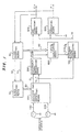
- Fig. 1 shows a circuit configuration of an interpolation pulse generating device according to an embodiment of the invention.
- the adjacent two phases selecting means includes means for generating sine-wave signals of M phases and means for selecting adjacent signals.
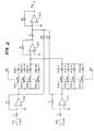
- Fig. 2 shows a preferred example of a circuit of the means 300. This circuit generates only one of the signals S j and S j-1 , but a circuit for generating the other signal can be constructed in the same manner with an exception that the orders of resistors (described below) are shifted by one.
- the circuit of Fig. 2 consists of an inverting amplifier 303 receiving the detection signal 100, parallel-connected analog switching elements 304-1 to 304-M, resistors 305-1 to 305-M that are connected in series to the respective analog switching elements 304-1 to 304-M, an inverting amplifier 317 receiving the detection signal 200, parallel-connected analog switching elements 318-1 to 318-M, resistors 319-1 to 319-M that are connected in series to the respective analog switching elements 318-1 to 318-M, and inverting amplifiers 307 and 310.
- One of the resistors 305-1 to 305-M and one of the resistors 319-1 to 319-M are selected by the analog switching elements 304-1 to 304-M and 318-1 to 318-M in accordance with an output signal 80 of an M-ary counting means (M-ary reversible ring counter) 70.
- the selected resistors and the inverting amplifier 307 constitute a two-input addition type variable gain amplifier.
- the resistances of the resistors 305-1 to 305-M are represented by R 11 to R 1M and the resistances of the resistors 319-1 to 319-M are represented by R 21 to R 2M .
- analog switching elements 304-j and 318-j are turned on. In this state, an output signal of the inverting amplifier 307 is obtained as follows: R ⁇ Vsin ⁇ /R 1j + R ⁇ Vcos ⁇ /R 2j
- An output S j of the inverting amplifier 310 is equal to an inverted sum of the output signal of the inverting amplifier 307 multiplied by 2, the output signal of the inverting amplifier 303 (-Vsin ⁇ ), and the output signal of the inverting amplifier 317 (-Vcos ⁇ ).
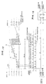
- Fig. 5 is a timing chart of the respective signals.
- the vertical axes represent voltages and the horizontal axes represent the movement distance.
- each of the signal S j- 1 (see part (b) of Fig. 5) and the signal S j (see part (c) of Fig. 5) forms a triangle in the vicinity of the zero level.
- nR 0 and R 0 represent resistances and reference numeral 501 denotes an operational amplifier.
- the value of ⁇ S j is almost constant.
- the difference signal ⁇ S j /n is input to a k ⁇ S j /n generating means 600.
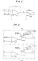
- Fig. 4 shows a specific circuit configuration of the means 600.
- Output signals 90 (9 1 , 9 2 , ..., 9 k , ..., 9 n ) of an n-ary counting means (n-ary reversible ring counter) 60 are supplied to analog switching elements T 1 , T 2 , ..., T k , ..., T n as control signals for determining conduction/non-conduction thereof so that one of the switching elements T 1 -T n is made conductive and the other ones are made non-conductive.
- only the analog switching element T k is in a conductive state.
- a resistor having a resistance (1/k)q is provided between the analog switching element T k and an operational amplifier 601, which has a resistor having a resistance q.
- the operational amplifier 601 produces an output signal -k ⁇ S j /n.
- the signals -k ⁇ S j /n and S j-1 are input to a judgment signal generating means 700, which performs computation and produces a judgment signal S x according to Equation (8):
- Fig. 6 shows a specific circuit configuration of the judgment signal generating means 700.
- r s denotes resistors
- numerals 701 and 702 denote operational amplifiers.
- the signal S x is input to first and second comparing means 800 and 900.
- the first comparing means 800 compares S x and 0, and the second comparing circuit 900 compares S x and ⁇ S j /n.
- Fig. 7 shows specific circuit configurations of the comparing means 800 and 900.
- reference numerals 801 and 901 denote comparators, and F/F1 and F/F2 denote flip-flops.
- the output of the flip-flop F/F1 or F/F2 changes from "0" to "1" at a rising edge of a 0-to-1 change of the output of the comparator 801 or 901 in response to a change of the signal S x .
- the n-ary counting means 60 counts up or down at a rising edge of a 0-to-1 change of the output of the flip-flop F/F1 or F/F2.
- the analog switching elements T 1 -T n of the k ⁇ S j /n generating means 600 are switched in accordance with the output signals 90 of the n-ary counting means 60. Further, by making the CL input of the flip-flop F/F1 or F/F2 negative with a certain delay by use of a delay element, the output thereof changes from "1" to "0.” Thus, pulses P + and P - can be generated. By providing a delay, spike noise can be neglected which occurs at switching of the analog switching elements T 1 -T n .
- S j and S j-1 vary accordingly, and thereby transition is made from a state of S x ⁇ ⁇ S j /n to a state of S x > ⁇ S j /n.
- an output pulse P + is obtained from the second comparing means 900.
- the pulse P + is input to the n-ary counting means 60, a state of S x ⁇ ⁇ S j /n is re-established in response to a transition of k ⁇ k+1.
- a carry pulse 50 or a borrow pulse 51 is generated by the n-ary counting means 60 and input to the M-ary counting means 70, where a transition of j ⁇ j+1 or j ⁇ j-1 is effected.
- a feedback loop may be so formed that the signal S x always satisfy S x ⁇ 0 and S x > - ⁇ S j /n.
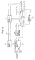
- Fig. 10 shows the entire configuration of the interpolation pulse generating device of this embodiment. Since the M-ary counting means 70 and the adjacent two phases selecting means 300, which together perform the M-division operation, are the same as those in the above embodiment (see Fig. 1), the following description is dedicated to the digital n-division technique.
- the signals ⁇ S j and - ⁇ S j are input to an A/D converter 1100 as positive and negative references, respectively.
- the A/D converter 1100 constitutes a bipolar A/D converter.
- Fig. 11 shows a relationship between an input voltage and output data of the A/D converter 1100. For simplicity, only upper 4 bits of output data are shown in Fig. 11.
- the output signal S j-1 of the adjacent two phases selecting means 300 is converted into a digital code by the A/D converter 1100 according to the relationship of Fig. 11.
- the digitized signal S j-1 is input to a comparing circuit 1200, where it is compared with the value of a signal supplied from an n-ary counting means 61. Now the inputs from the n-ary counting means 61 and the A/D converter 1100 are represented by A and B, respectively.
- the comparing circuit 1200 makes the A>B output "true” when A > B, and makes the A ⁇ B output "true” when A ⁇ B.
- the A>B output and the A ⁇ B output are ANDed with a timing signal 1310 from a timing generating circuit 1300, so that a pulse P + or P - is produced.
- the n-ary counting means 61 is constituted of an up/down reversible counter.
- the n-ary counting means 61 changes its count value from k to k+1.
- the input A of the comparator 1210 is updated accordingly, and compared with the input B at the next timing.
- the n-ary counting means 61 changes its count value from k to k-1.
- a carry pulse 50 or a borrow pulse 51 is generated and input to the M-ary counting means 70.
- the M-ary counting means 70 changes its count value j to j+1 or j-1.
- Fig. 11 shows only upper 4 bits of output data of the A/D converter 1100 and plots a straight line, though actually the output data are discrete. Since n is equal to 4, it is assumed that the n-ary counting means 61 is constituted of a 2-bit binary reversible counter. It is also assumed that the A/D converter 1100 and the comparator 1210 deal with x+1-bit data.
- Fig. 14 shows how each of the A/D converter 1100 and the n-ary counting means 61 is connected to the comparator 1210.
- the bits of the A/D converter 1100 and those of the comparator 1210 (B input bits) are in one-to-one correspondence.
- the 2 x bit is always set "true” (has a value "1")
- the 2 x-1 bit and the 2 x-2 bit are allocated to the 2-bit input from the n-ary counting means 61
- the remaining lower bits are always set "false” (has a value "0").
- the interpolation pulse generating device will be described with reference to Fig. 13. It is assumed that at first the signal S j-1 as digitized by the A/D converter 1100 is (1000).%) 2 , i.e., 0 V, and the count value k of the n-ary counting means 61 is (00) 2 , and that the phase angles of the detection signals 100 and 200 vary at a constant rate. In this case, as indicated by symbol B in Fig. 13, the output of the A/D converter 1100, i.e., the input B of the comparing circuit 1200 increases with an approximately constant slope in a phase section of 2 ⁇ /M.
- the comparing circuit 1200 compares the input B with the input A, i.e., the output of the n-ary counting means 61 in synchronism with the timing signal 1310 that is supplied from the pulse generating circuit 1300.
- the comparing circuit 1200 outputs a pulse P + or P - based on the result of comparison between the output values of the A/D converter 1100 and the n-ary counting means 61.
- the count value of the n-ary counting means 61 changes from (11) 2 to (00) 2 .
- the n-ary counting means 61 produces a carry pulse 50, so that the count value of the M-ary counting means 70 changes from j to j+1.
- the count value of the n-ary counting means 61 changes from (00) 2 to (11) 2 .
- the n-ary counting means 61 produces a borrow pulse 51, so that the count value of the M-ary counting means 70 changes from j to j-1.
- n is assumed to be 4, and therefore the n-ary counting means 61 is implemented as a 2-bit binary reversible counter. Further, the 2 x bit of the A input bits of the comparator 1210 is always set “true” (has a value "1") and the output of the n-ary counting means 61 is supplied to the 2 x-1 and 2 x-2 bit terminals.
- the above embodiment can easily accommodate a case where n is larger than 4 by changing the connection for the input A of the comparator 1210 as long as n is a certain power of 2.
- the reference signal is obtained by performing a computation on the input signals, i.e., detection signals Vsin ⁇ and Vcos ⁇ . It may be conceived to simply use a constant voltage generator or the like instead of the reference signal ⁇ S j , which is approximately constant theoretically as shown in part (e) of Fig. 5. However, the amplitude V of the detection signals Vsin ⁇ and Vcos ⁇ that are output from the detector may vary due to a temperature variation or a variation in performance of the operational amplifiers.
- the reference signal for comparison with the judgment signal S x is so generated as to vary in proportion to the amplitude V of the signals S j and S j-1 as in the case of ⁇ S j in the above embodiment, the influence on the interpolation pitch error can greatly be reduced, which enables provision of an interpolation pulse generating device having high accuracy and resolution.
- the interpolation is performed in two stages, i.e., M-division and n-division, and it is utilized that a sine wave can be regarded as approximately straight in the vicinity of a phase 0°. Therefore, a simple, less expensive interpolation pulse generating device that operates at high speed and has high accuracy and resolution can be provided by using a smaller number of high-accuracy resistors and switching circuits of two stages (M and n).
Landscapes
- Engineering & Computer Science (AREA)
- Theoretical Computer Science (AREA)
- Physics & Mathematics (AREA)
- General Physics & Mathematics (AREA)
- Transmission And Conversion Of Sensor Element Output (AREA)
- Complex Calculations (AREA)
Claims (9)
- Vorrichtung zum Erzeugen von Interpolationsimpulsen, die Detektorsignale mit einer Vielzahl von Phasen empfängt, die in Übereinstimmung mit der relativen Bewegungsverschiebung zwischen entsprechenden Gliedern erzeugt werden, und einen Zählimpuls für jeden vorbestimmten Phasenwinkelabstand erzeugt, der kleiner ist als eine Periode der Detektorsignale, wobei die Vorrichtung umfasst:eine Auswahleinrichtung (300) zum Erzeugen von Signalen Sj und Sj-1, die voneinander um einen Phasenwert von 2π/M abweichen, indem die Vielzahl von Detektorsignalen kombiniert werden, wobei M eine festgelegte ganze Zahl ist,eine Differenzsignalerzeugungseinrichtung (500) zum Erzeugen einer Bezugssignals ΔS, das eine Differenz zwischen den Signalen Sj und Sj-1 wiedergibt, undeine Vergleichseinrichtung (800) zum Erzeugen eines Aufwärtsimpulses oder eines Abwärtsimpulses, jedes Mal wenn das Signal Sj oder Sj-1 um ΔS/n variiert, wobei n eine festgelegte ganze Zahl in einem Phasenabschnitt von 2π/M ist, in dem eines der Signale Sj und Sj-1 einen positiven Wert und das andere Signal einen negativen Wert aufweist.
- Vorrichtung zum Erzeugen von Interpolationsimpulsen nach Anspruch 1, wobei die Auswahleinrichtung (300) zwei sinusförmige Detektorsignale empfängt, die dieselbe Amplitude, dieselbe räumliche Periode und eine vorbestimmte räumliche Phasendifferenz aufweisen und symmetrisch in Bezug auf eine Nullebene variieren, und wobei die Auswahleinrichtung aus den M sinusförmigen Signalen S1-SM, die voneinander mit vorbestimmten Intervallen abweichen, wobei eine ganze Zahl J = 1, 2, ... M ist, die Signale Sj und Sj-1 auswählt, indem sie die zwei sinusförmigen Detektorsignale kombiniert.
- Vorrichtung zum Erzeugen von Interpolationsimpulsen nach Anspruch 1 oder Anspruch 2, die weiterhin umfasst:eine n-äre Zähleinrichtung (60) zum Ausgeben eines ersten Zählwerts und eines Übertrags- oder Borgeimpulses, indem sie die Aufwärtsimpulse und die Abwärtsimpulse zählt, wobei der erste Zählwert verwendet wird, um die Vergleichseinrichtung zu steuern, undeine M-äre Zähleinrichtung (70) zum Ausgeben eines zweiten Zählwerts, indem die Übertrags- und Borgeimpulse gezählt werden, wobei der zweite Zählwert verwendet wird, um die Auswahleinrichtung zu steuern.
- Vorrichtung zum Erzeugen von Interpolationsimpulsen nach wenigstens einem der vorstehenden Ansprüche, wobei die Differenzsignalerzeugungseinrichtung (500) ein Differenzsignal ΔSj/n in Übereinstimmung mit der folgenden Gleichung erzeugt:
- Vorrichtung zum Erzeugen von Interpolationsimpulsen nach wenigstens einem der vorstehenden Ansprüche, wobei die Vorrichtung weiterhin umfasst:eine kΔSj/n-Erzeugungseinrichtung (600) zum Erzeugen eines Signals kΔSj/n, wobei k eine ganze Zahl ist, undeine Entscheidungssignalerzeugungseinrichtung (700), um auf der Basis des sinusförmigen Detektorsignals Sj-1 und des Signals kΔSn/n ein Entscheidungssignal Sx in Übereinstimmung mit der folgenden Gleichung zu erzeugen:eine erste Vergleichseinrichtung (800) zum Ausgeben eines Abwärtsimpulses P-, wenn das Entscheidungssignal Sx kleiner ist als 0, undeine zweite Vergleichseinrichtung (900) zum Ausgeben eines Aufwärtsimpulses P+, wenn das Entscheidungssignal Sx größer ist als ΔSj/n.
- Vorrichtung zum Erzeugen von Interpolationsimpulsen nach wenigstens einem der Ansprüche 1 bis 4, wobei die Vorrichtung weiterhin umfasst:eine kΔSj/n-Erzeugungseinrichtung (600) zum Erzeugen eines Signals kΔSj/n, wobei k eine ganze Zahl ist,eine Entscheidungssignalerzeugungseinrichtung (700), um auf der Basis des sinusförmigen Detektorsignals Sj-1 und des Signals kΔSn/n ein Entscheidungssignal Sx in Übereinstimmung mit der folgenden Gleichung zu erzeugen:eine erste Vergleichseinrichtung (800) zum Ausgeben eines Abwärtsimpulses P-, wenn das Entscheidungssignal Sx kleiner ist als - ΔSj/n, undeine zweite Vergleichseinrichtung (900) zum Ausgeben eines Aufwärtsimpulses P+, wenn das Entscheidungssignal Sx größer ist als 0.
- Vorrichtung zum Erzeugen von Interpolationsimpulsen nach Anspruch 5 oder 6 bei Abhängigkeit von wenigstens Anspruch 3, wobei die n-äre Zähleinrichtung (60) dafür ausgebildet ist, die ganze Zahl k um 1 zu dekrementieren, wenn der Abwärtsimpuls P-empfangen wird, und wenn das dekrementierte Ergebnis gleich 0 ist, n in k einzusetzen und einen Borgeimpuls auszugeben, sowie die ganze Zahl k um 1 zu inkrementieren, wenn der Aufwärtsimpuls P+ empfangen wird, und wenn das inkrementierte Ergebnis gleich n + 1 ist, 1 in k einzusetzen und einen Übertragimpuls auszugeben, um anzugeben, dass die ganze Zahl k an die kΔSj/n-Erzeugungseinrichtung ausgegeben wird, und wobei die
M-äre Zähleinrichtung (70) dafür ausgebildet ist, die ganze Zahl j um 1 zu dekrementieren, wenn der Borgeimpuls empfangen wird, und wenn das dekrementierte Ergebnis gleich 0 ist, M in j einzusetzen, sowie die ganze Zahl j um 1 zu inkrementiere, wenn der Übertragimpuls empfangen wird, und wenn das inkrementierte Ergebnis gleich M + 1 ist, 1 in j einzusetzen, um anzugeben, dass die ganze Zahl j an die Auswahleinrichtung ausgegeben wird. - Vorrichtung zum Erzeugen von Interpolationsimpulsen, die Detektorsignale mit einer Vielzahl von Phasen empfängt, die in Übereinstimmung mit der relativen Bewegungsverschiebung zwischen entsprechenden Gliedern erzeugt werden, und einen Zählimpuls für jeden vorbestimmten Phasenwinkelabstand erzeugt, der kleiner ist als eine Periode der Detektorsignale, wobei die Vorrichtung umfasst:eine Auswahleinrichtung (300) zum Empfangen von zwei sinusförmigen Detektorsignalen, die dieselbe Amplitude, dieselbe räumliche Periode und eine vorbestimmte räumliche Phasendifferenz aufweisen und symmetrisch in Bezug auf eine Nullebene variieren, und zum Auswählen der Signale Sj und Sj-1 aus den M sinusförmigen Signalen S1-SM, die durch voneinander durch vorbestimmte Intervalle abweichen, wobei eine ganze Zahl J = 1, 2, ... M ist, indem sie die zwei sinusförmigen Detektorsignale kombiniert,eine Differenzsignalerzeugungseinrichtung (520) zum Erzeugen eines Differenzsignals Δsj in Übereinstimmung mit der folgenden Gleichung:eine A/D-Wandlereinrichtung (1100) zum A/D-Wandeln des sinusförmigen Signals Sj-1 unter Verwendung der Signale ΔSj und -ΔSj als Bezugssignale,eine Vergleichseinrichtung (1200) zum Vergleichen einer Ausgabe A einer n-ären Zähleinrichtung und einer Ausgabe B einer A/D-Wandlereinrichtung sowie zum Ausgeben eines Aufwärtsimpulses P+, wenn die Ausgabe A kleiner oder gleich der Ausgabe B ist, und zum Ausgeben eines Abwärtsimpulses P-, wenn die Ausgabe A größer ist als die Ausgabe B,die n-äre Zähleinrichtung (61) zum Dekrementieren der ganzen Zahl j um 1, wenn der Abwärtsimpuls P- empfangen wird, und wenn das dekrementierte Ergebnis kleiner als 0 ist, zum Einsetzen von n - 1 in k und zum Ausgeben eines Borgeimpulses, sowie zum Inkrementieren der ganzen Zahl k um 1, wenn der Aufwärtsimpuls P+ empfangen wird, und wenn das inkrementierte Ergebnis gleich n ist, zum Einsetzen von 0 in k und zum Ausgeben eines Übertragsimpulses, um anzugeben, dass die ganze Zahl k als Ausgabe A an die Vergleichseinrichtung ausgegeben wird, undeine M-äre Zähleinrichtung (70) zum Dekrementieren der ganzen Zahl j um 1, wenn der Borgeimpuls empfangen wird, und wenn das dekrementierte Ergebnis gleich 0 ist, zum Einsetzen von M in j, sowie zum Inkrementieren der ganzen Zahl j um 1, wenn der Übertragsimpuls empfangen wird, und wenn das inkrementierte Ergebnis gleich M + 1 ist, zum Einsetzen von 1 in j, um anzugeben, dass die ganze Zahl k zu der Auswahleinrichtung ausgegeben wird.
- Vorrichtung zum Erzeugen von Interpolationsimpulsen nach Anspruch 8, die weiterhin eine Dämpfereinrichtung umfasst, um einen Count-Up-lmpuls nur dann zu erzeugen, wenn der Aufwärtsimpuls P+ aufeinanderfolgend erzeugt wird, und um einen Count-Down-lmpuls nur dann zu erzeugen, wenn der Abwärtsimpuls P- aufeinanderfolgend erzeugt wird, wobei der Count-Up-lmpuls und der Count-Down-lmpuls anstelle des Aufwärtsimpulses P+ und des Abwärtsimpulses P- jeweils an die Vergleichseinrichtung ausgegeben werden.
Applications Claiming Priority (3)
| Application Number | Priority Date | Filing Date | Title |
|---|---|---|---|
| JP29901094 | 1994-11-08 | ||
| JP6299010A JP2756761B2 (ja) | 1994-11-08 | 1994-11-08 | 内挿パルス発生装置 |
| JP299010/94 | 1994-11-08 |
Publications (3)
| Publication Number | Publication Date |
|---|---|
| EP0711974A2 EP0711974A2 (de) | 1996-05-15 |
| EP0711974A3 EP0711974A3 (de) | 1996-11-20 |
| EP0711974B1 true EP0711974B1 (de) | 2001-09-26 |
Family
ID=17867068
Family Applications (1)
| Application Number | Title | Priority Date | Filing Date |
|---|---|---|---|
| EP95307756A Expired - Lifetime EP0711974B1 (de) | 1994-11-08 | 1995-10-31 | Vorrichtung zur Erzeugung von Interpolationspulsen |
Country Status (5)
| Country | Link |
|---|---|
| US (1) | US5734688A (de) |
| EP (1) | EP0711974B1 (de) |
| JP (1) | JP2756761B2 (de) |
| CN (1) | CN1050663C (de) |
| DE (1) | DE69522897T2 (de) |
Cited By (1)
| Publication number | Priority date | Publication date | Assignee | Title |
|---|---|---|---|---|
| DE10208915A1 (de) * | 2002-01-11 | 2003-07-24 | Heidenhain Gmbh Dr Johannes | Verfahren zur Interpolation mindestens zweier positionsabhängiger, periodischer, zueinander phasenverschobener Analogsignale |
Families Citing this family (3)
| Publication number | Priority date | Publication date | Assignee | Title |
|---|---|---|---|---|
| JP2927278B2 (ja) * | 1997-08-06 | 1999-07-28 | 日本電気株式会社 | 不連続信号内挿回路 |
| EP1468496B1 (de) * | 2002-01-11 | 2006-03-08 | Dr. Johannes Heidenhain GmbH | Verfahren zur interpolation mindestens zweier positionsabhängiger, periodischer, zueinander phasenverschobener analogsignale |
| JP6649018B2 (ja) * | 2015-09-16 | 2020-02-19 | 日本電産サンキョー株式会社 | ロータリエンコーダ、およびロータリエンコーダの絶対角度位置検出方法 |
Family Cites Families (12)
| Publication number | Priority date | Publication date | Assignee | Title |
|---|---|---|---|---|
| DE2729697A1 (de) * | 1977-07-01 | 1979-01-04 | Heidenhain Gmbh Dr Johannes | Verfahren zur interpolation |
| JPS6037711B2 (ja) * | 1978-09-01 | 1985-08-28 | 株式会社東芝 | 位相検出器 |
| JPS5643506A (en) | 1979-09-17 | 1981-04-22 | Mitsutoyo Mfg Co Ltd | Multidivided circuit of length measuring machine |
| JPS63186109A (ja) | 1987-01-27 | 1988-08-01 | Mitsutoyo Corp | 測定装置の補間回路 |
| US4814704A (en) * | 1987-04-08 | 1989-03-21 | Motorola, Inc. | Rotor position indicator with correction for apparant acceleration and deceleration |
| JP2649390B2 (ja) * | 1988-10-12 | 1997-09-03 | キヤノン株式会社 | 信号内挿回路 |
| US5123742A (en) * | 1989-06-07 | 1992-06-23 | Hitachi Electronics Engineering Co., Ltd. | Laser length measuring instrument |
| EP0414953B1 (de) * | 1989-09-01 | 1993-07-07 | Kabushiki Kaisha S.G. | Positionswertgeber |
| US5452425A (en) * | 1989-10-13 | 1995-09-19 | Texas Instruments Incorporated | Sequential constant generator system for indicating the last data word by using the end of loop bit having opposite digital state than other data words |
| US5218295A (en) * | 1991-04-15 | 1993-06-08 | Kayaba Kogyo Kabushiki Kaisha | System for processing position signals to improve resolution of the position of an object |
| JP3110530B2 (ja) * | 1991-11-22 | 2000-11-20 | 株式会社エスジー | 位置検出装置及び時間測定装置 |
| JP3232795B2 (ja) * | 1992-08-06 | 2001-11-26 | キヤノン株式会社 | 検出装置 |
-
1994
- 1994-11-08 JP JP6299010A patent/JP2756761B2/ja not_active Expired - Fee Related
-
1995
- 1995-10-27 US US08/549,143 patent/US5734688A/en not_active Expired - Fee Related
- 1995-10-31 EP EP95307756A patent/EP0711974B1/de not_active Expired - Lifetime
- 1995-10-31 DE DE69522897T patent/DE69522897T2/de not_active Expired - Fee Related
- 1995-11-07 CN CN95118284A patent/CN1050663C/zh not_active Expired - Fee Related
Cited By (1)
| Publication number | Priority date | Publication date | Assignee | Title |
|---|---|---|---|---|
| DE10208915A1 (de) * | 2002-01-11 | 2003-07-24 | Heidenhain Gmbh Dr Johannes | Verfahren zur Interpolation mindestens zweier positionsabhängiger, periodischer, zueinander phasenverschobener Analogsignale |
Also Published As
| Publication number | Publication date |
|---|---|
| EP0711974A3 (de) | 1996-11-20 |
| CN1155068A (zh) | 1997-07-23 |
| US5734688A (en) | 1998-03-31 |
| DE69522897T2 (de) | 2002-04-04 |
| EP0711974A2 (de) | 1996-05-15 |
| CN1050663C (zh) | 2000-03-22 |
| DE69522897D1 (de) | 2001-10-31 |
| JPH08136280A (ja) | 1996-05-31 |
| JP2756761B2 (ja) | 1998-05-25 |
Similar Documents
| Publication | Publication Date | Title |
|---|---|---|
| US6556153B1 (en) | System and method for improving encoder resolution | |
| CN109696112B (zh) | 用于电感式绝对位置编码器的紧凑型伪随机标尺和读头 | |
| US5907298A (en) | Interpolation circuit for encoder | |
| US6384752B1 (en) | Absolute encoder | |
| US9030194B2 (en) | Position encoder apparatus | |
| US9766095B2 (en) | Magnetic position detection device and magnetic position detection method | |
| EP1236973B1 (de) | Verfahren zur Veränderung von Interpolationsfaktoren | |
| US8271221B2 (en) | Phase detection device and position detection device | |
| EP1761743B1 (de) | Anordnung mit einem magnetfeldsensor | |
| JP4052797B2 (ja) | 位置のディジタル検知器 | |
| EP0711974B1 (de) | Vorrichtung zur Erzeugung von Interpolationspulsen | |
| US9927234B2 (en) | Position-measuring device and method for operating the same | |
| US7099790B2 (en) | Sensor signal processor | |
| JP3008503B2 (ja) | 位置検出装置 | |
| CN109844462B (zh) | 增量型编码器的脉冲化变换装置及脉冲化变换方法 | |
| EP0455984A1 (de) | Koordinatenmessmaschine mit verbesserter Interpolationsschaltung | |
| US7129698B2 (en) | Method and device for preparing a sensor signal of a position sensor for transmission to an evaluation unit | |
| CN110296722B (zh) | 一种磁编码器的编码方法和磁编码器 | |
| JP3365913B2 (ja) | 位置検出装置 | |
| KR100384173B1 (ko) | 모터 제어용 고분해능 인코더 신호 처리장치 및 그 방법 | |
| CN112268501B (zh) | 一种可应用于物体线性位移或转角位置的检测方法 | |
| JPH0658769A (ja) | 信号処理方法及びそれを用いた変位検出装置 | |
| JP3015751B2 (ja) | エンコーダの内挿回路 | |
| CN100535604C (zh) | 电子细分割装置及其方法 | |
| JPH0721421B2 (ja) | 矩形波信号の評価回路 |
Legal Events
| Date | Code | Title | Description |
|---|---|---|---|
| PUAI | Public reference made under article 153(3) epc to a published international application that has entered the european phase |
Free format text: ORIGINAL CODE: 0009012 |
|
| AK | Designated contracting states |
Kind code of ref document: A2 Designated state(s): DE FR GB |
|
| PUAL | Search report despatched |
Free format text: ORIGINAL CODE: 0009013 |
|
| AK | Designated contracting states |
Kind code of ref document: A3 Designated state(s): DE FR GB |
|
| 17P | Request for examination filed |
Effective date: 19970509 |
|
| RAP1 | Party data changed (applicant data changed or rights of an application transferred) |
Owner name: MITUTOYO CORPORATION |
|
| 17Q | First examination report despatched |
Effective date: 19990720 |
|
| GRAG | Despatch of communication of intention to grant |
Free format text: ORIGINAL CODE: EPIDOS AGRA |
|
| GRAG | Despatch of communication of intention to grant |
Free format text: ORIGINAL CODE: EPIDOS AGRA |
|
| GRAH | Despatch of communication of intention to grant a patent |
Free format text: ORIGINAL CODE: EPIDOS IGRA |
|
| GRAH | Despatch of communication of intention to grant a patent |
Free format text: ORIGINAL CODE: EPIDOS IGRA |
|
| GRAA | (expected) grant |
Free format text: ORIGINAL CODE: 0009210 |
|
| RIN1 | Information on inventor provided before grant (corrected) |
Inventor name: OKAMOTO, KIYOKAZU, C/O MITUTOYO CORP. Inventor name: TERAGUCHI, MIKIYA, C/O MITUTOYO CORP. |
|
| AK | Designated contracting states |
Kind code of ref document: B1 Designated state(s): DE FR GB |
|
| REF | Corresponds to: |
Ref document number: 69522897 Country of ref document: DE Date of ref document: 20011031 |
|
| REG | Reference to a national code |
Ref country code: GB Ref legal event code: IF02 |
|
| ET | Fr: translation filed | ||
| PLBE | No opposition filed within time limit |
Free format text: ORIGINAL CODE: 0009261 |
|
| STAA | Information on the status of an ep patent application or granted ep patent |
Free format text: STATUS: NO OPPOSITION FILED WITHIN TIME LIMIT |
|
| 26N | No opposition filed | ||
| PGFP | Annual fee paid to national office [announced via postgrant information from national office to epo] |
Ref country code: GB Payment date: 20061025 Year of fee payment: 12 |
|
| PGFP | Annual fee paid to national office [announced via postgrant information from national office to epo] |
Ref country code: DE Payment date: 20061026 Year of fee payment: 12 |
|
| GBPC | Gb: european patent ceased through non-payment of renewal fee |
Effective date: 20071031 |
|
| PG25 | Lapsed in a contracting state [announced via postgrant information from national office to epo] |
Ref country code: DE Free format text: LAPSE BECAUSE OF NON-PAYMENT OF DUE FEES Effective date: 20080501 |
|
| REG | Reference to a national code |
Ref country code: FR Ref legal event code: ST Effective date: 20080630 |
|
| PGFP | Annual fee paid to national office [announced via postgrant information from national office to epo] |
Ref country code: FR Payment date: 20061010 Year of fee payment: 12 |
|
| PG25 | Lapsed in a contracting state [announced via postgrant information from national office to epo] |
Ref country code: GB Free format text: LAPSE BECAUSE OF NON-PAYMENT OF DUE FEES Effective date: 20071031 |
|
| PG25 | Lapsed in a contracting state [announced via postgrant information from national office to epo] |
Ref country code: FR Free format text: LAPSE BECAUSE OF NON-PAYMENT OF DUE FEES Effective date: 20071031 |