EP0710986A2 - Convertisseur photoélectrique - Google Patents
Convertisseur photoélectrique Download PDFInfo
- Publication number
- EP0710986A2 EP0710986A2 EP96200019A EP96200019A EP0710986A2 EP 0710986 A2 EP0710986 A2 EP 0710986A2 EP 96200019 A EP96200019 A EP 96200019A EP 96200019 A EP96200019 A EP 96200019A EP 0710986 A2 EP0710986 A2 EP 0710986A2
- Authority
- EP
- European Patent Office
- Prior art keywords
- signal
- photoelectric conversion
- circuit
- reading
- conversion element
- Prior art date
- Legal status (The legal status is an assumption and is not a legal conclusion. Google has not performed a legal analysis and makes no representation as to the accuracy of the status listed.)
- Granted
Links
- 238000006243 chemical reaction Methods 0.000 claims abstract description 120
- 238000003860 storage Methods 0.000 claims abstract description 68
- 239000000758 substrate Substances 0.000 claims abstract description 14
- 238000003491 array Methods 0.000 claims description 26
- 230000003287 optical effect Effects 0.000 claims description 19
- 230000005540 biological transmission Effects 0.000 claims description 2
- 230000007274 generation of a signal involved in cell-cell signaling Effects 0.000 claims 1
- 238000001514 detection method Methods 0.000 description 49
- 239000003990 capacitor Substances 0.000 description 27
- 239000010410 layer Substances 0.000 description 23
- 238000010276 construction Methods 0.000 description 16
- 238000010586 diagram Methods 0.000 description 14
- 239000012535 impurity Substances 0.000 description 13
- 230000000694 effects Effects 0.000 description 11
- 238000000034 method Methods 0.000 description 10
- 229910021420 polycrystalline silicon Inorganic materials 0.000 description 10
- 229920005591 polysilicon Polymers 0.000 description 10
- 238000004519 manufacturing process Methods 0.000 description 9
- XAGFODPZIPBFFR-UHFFFAOYSA-N aluminium Chemical compound [Al] XAGFODPZIPBFFR-UHFFFAOYSA-N 0.000 description 8
- 229910052782 aluminium Inorganic materials 0.000 description 8
- 230000008054 signal transmission Effects 0.000 description 8
- ZOXJGFHDIHLPTG-UHFFFAOYSA-N Boron Chemical compound [B] ZOXJGFHDIHLPTG-UHFFFAOYSA-N 0.000 description 5
- 229910052796 boron Inorganic materials 0.000 description 5
- OAICVXFJPJFONN-UHFFFAOYSA-N Phosphorus Chemical compound [P] OAICVXFJPJFONN-UHFFFAOYSA-N 0.000 description 4
- 229910052698 phosphorus Inorganic materials 0.000 description 4
- 239000011574 phosphorus Substances 0.000 description 4
- 239000004065 semiconductor Substances 0.000 description 4
- 238000009792 diffusion process Methods 0.000 description 3
- 238000005070 sampling Methods 0.000 description 3
- XUIMIQQOPSSXEZ-UHFFFAOYSA-N Silicon Chemical compound [Si] XUIMIQQOPSSXEZ-UHFFFAOYSA-N 0.000 description 2
- 230000002411 adverse Effects 0.000 description 2
- IZJSTXINDUKPRP-UHFFFAOYSA-N aluminum lead Chemical compound [Al].[Pb] IZJSTXINDUKPRP-UHFFFAOYSA-N 0.000 description 2
- 229910052785 arsenic Inorganic materials 0.000 description 2
- RQNWIZPPADIBDY-UHFFFAOYSA-N arsenic atom Chemical compound [As] RQNWIZPPADIBDY-UHFFFAOYSA-N 0.000 description 2
- 230000000903 blocking effect Effects 0.000 description 2
- 230000006870 function Effects 0.000 description 2
- 238000005468 ion implantation Methods 0.000 description 2
- 238000002955 isolation Methods 0.000 description 2
- 239000004973 liquid crystal related substance Substances 0.000 description 2
- 230000003071 parasitic effect Effects 0.000 description 2
- 239000011241 protective layer Substances 0.000 description 2
- 229910052710 silicon Inorganic materials 0.000 description 2
- 239000010703 silicon Substances 0.000 description 2
- 229910052581 Si3N4 Inorganic materials 0.000 description 1
- 230000015572 biosynthetic process Effects 0.000 description 1
- 239000000969 carrier Substances 0.000 description 1
- 238000000151 deposition Methods 0.000 description 1
- 239000011521 glass Substances 0.000 description 1
- 238000005286 illumination Methods 0.000 description 1
- 229910010272 inorganic material Inorganic materials 0.000 description 1
- 239000011147 inorganic material Substances 0.000 description 1
- 238000009413 insulation Methods 0.000 description 1
- 229910052757 nitrogen Inorganic materials 0.000 description 1
- 239000011368 organic material Substances 0.000 description 1
- 238000007254 oxidation reaction Methods 0.000 description 1
- 238000000059 patterning Methods 0.000 description 1
- 230000011514 reflex Effects 0.000 description 1
- 230000004044 response Effects 0.000 description 1
- HQVNEWCFYHHQES-UHFFFAOYSA-N silicon nitride Chemical compound N12[Si]34N5[Si]62N3[Si]51N64 HQVNEWCFYHHQES-UHFFFAOYSA-N 0.000 description 1
Images


Classifications
-
- H—ELECTRICITY
- H01—ELECTRIC ELEMENTS
- H01L—SEMICONDUCTOR DEVICES NOT COVERED BY CLASS H10
- H01L27/00—Devices consisting of a plurality of semiconductor or other solid-state components formed in or on a common substrate
- H01L27/14—Devices consisting of a plurality of semiconductor or other solid-state components formed in or on a common substrate including semiconductor components sensitive to infrared radiation, light, electromagnetic radiation of shorter wavelength or corpuscular radiation and specially adapted either for the conversion of the energy of such radiation into electrical energy or for the control of electrical energy by such radiation
- H01L27/144—Devices controlled by radiation
- H01L27/146—Imager structures
- H01L27/14643—Photodiode arrays; MOS imagers
-
- H—ELECTRICITY
- H01—ELECTRIC ELEMENTS
- H01L—SEMICONDUCTOR DEVICES NOT COVERED BY CLASS H10
- H01L27/00—Devices consisting of a plurality of semiconductor or other solid-state components formed in or on a common substrate
- H01L27/14—Devices consisting of a plurality of semiconductor or other solid-state components formed in or on a common substrate including semiconductor components sensitive to infrared radiation, light, electromagnetic radiation of shorter wavelength or corpuscular radiation and specially adapted either for the conversion of the energy of such radiation into electrical energy or for the control of electrical energy by such radiation
- H01L27/144—Devices controlled by radiation
- H01L27/146—Imager structures
- H01L27/14681—Bipolar transistor imagers
Definitions
- This invention relates to photoelectric converters and, more particularly, to a photoelectric converter, which comprises a plurality of photoelectric conversion elements capable of storing photoelectrically produced charge. More specifically, the invention concerns a photoelectric converter, which can be suitably used for passive focus detectors for optical apparatuses such as cameras, slide projectors and liquid crystal projectors.
- Figure 14 shows an equivalent circuit diagram of a photoelectric conversion element array shown in Japanese Patent Laid-Open Application No. 1-222583.
- phototransistors or cells of storage type. These phototransistors have such a structure that their collector is connected to a common power supply, and they can store photoelectrically produced charge in their control electrode area (i.e., base) and let stored charge be read out from their main electrode area (i.e., emitter).
- control electrode area i.e., base
- main electrode area i.e., emitter
- the structure is described in detail in Japanese Patent Laid-Open Application No. 62-128678, Japanese Patent Laid-Open Application No. 62-113468, Japanese Patent Laid-Open Application No. 63-24664, Japanese Patent Laid-Open Application No. 63-76476 and Japanese Patent Laid-Open Application No. 63-76582.
- Designated at 2-1 to 2-n are PMOS switches for resetting the bipolar transistors of phototransistor array 1 by connecting the bases thereof to power supply V c when ⁇ res is given, at 3-1 to 3-n are NMOS switches each connected to the emitter of each bipolar transistor for taking out stored signal to the following stage in synchronism to ⁇ t , at 4-1 to 4-n NMOS switches each connected in series with each of NMOS switches 3-1 to 3-n for sending out image signal to read line 7, and at 5-1 to 5-n are storage capacitors each for reading out signal for each of pixels connected between points of connection between NMOS switches 3-1 to 3-n and 4-1 to 4-n and ground.
- Designated at 6 is a shift register for reading out image signal by sequentially turning on NMOS switches 4-1 to 4-n, 8 a NMOS switch for connecting read line 7, to which output terminals of NMOS switches 4-1 to 4-n are commonly connected, to ground for initialization when signal ⁇ nrs is given, and at 9 is an output amplifier for amplifying image signal output to read line 7.
- Designated at 10-1 to 10-n are NMOS switches for grounding the emitter of each of phototransistors 1-1 to 1-n when ⁇ vrs is given.
- Designated at 107 is a maximum/minimum value detection circuit, which includes maximum value detection circuits 11-1 to 11-n, minimum value detection circuits 12-1 to 12-n and output amplifiers 13 and 14.
- Figure 15 shows the structure of one minimum value detection circuit.
- one minimum value detection circuit is constituted by a single differential amplifier 30 and a single pnp transistor 31.
- Differential amplifier 30 is constituted by constant current circuit 411, PMOS transistors 407 and 408 and NMOS transistors 409 and 410.
- the emitter line of pnp transistor 31 is fed back to inversion input terminal In2 of differential amplifier 30, and to non-inversion input terminal In1 thereof is connected each emitter of the pixel array of phototransistors 1-1 to 1-n.
- the base potential on pnp transistor 31 is changed substantially to the power supply voltage level to turn off pnp transistor 31. In consequence, no voltage is provided as input to output amplifier 13 shown in Figure 14.
- pnp transistor 31 produces an output voltage, which is indicative of detection of the minimum value.
- Figure 16 shows the structure of one maximum value detection circuit.
- one maximum value detection circuit is constituted by a single differential amplifier 32 and a single npn transistor 33.
- Differential amplifier 32 is constituted by constant current circuit 401, PMOS transistors 402 and 403 and NMOS transistors 404 and 405.
- the emitter line of npn transistor 33 is fed back to inversion input terminal In2 of differential amplifier 32 and also to an output line.
- To non-inversion input terminal In1 is connected each emitter of each pixel row.
- the base potential on npn transistor 33 is lowered substantially to the voltage level of negative power supply, thus turning off npn transistor 33.
- npn transistor 33 produces an output voltage, which is indicative of detection of the maximum value.
- load resistance is denoted by R.
- Figure 17 is a timing chart for explaining the operation of the photoelectric conversion element array shown in Figure 14.
- ⁇ vrs and ⁇ t are held at high level (i.e., "on") from instant t3 to instant t4, thus turning on NMOS switches 10-1 to 10-n and 3-1 to 3-n to ground storage capacitors 5-1 to 5-n and reset residual charge.
- NMOS switches 4-1 to 4-n are sequentially turned on by shift register 6, thus reading out signal charges stored in storage capacitors 5-1 to 5-n to read line 7.
- Shift register 6 selects NMOS switches 4-1 to 4-n one by one each time when ⁇ ck is given.
- NMOS switch 8 is turned on under control of ⁇ nrs to reset charge remaining on read line 7.
- Japanese Patent Laid-Open Application No. 63-47644 proposes a method of performing A/D conversion of only featuring portions of an object pattern through storage time control such as to make constant the difference between bright and dark portions of the pattern by constructing a photoelectric converter as shown in Figures 18 and 19 with a photoelectric conversion element array provided with maximum and minimum value detection circuits as noted above.
- a check as to whether storage is performed up to an adequate level is done through a check as to whether reference level V ref is reached by the difference between maximum and minimum values of storage level of the photoelectric conversion element array.
- Designated at 102 is a differential amplifier for taking the difference between V max and V min
- 103 is a comparator for comparing the output of differential amplifier 102 to predetermined reference level V ref to determine the reaching of adequate storage level.
- signal ⁇ comp of comparator 103 is inverted
- microcomputer 104 detects the reaching of the reference level of storage and provides pulse ⁇ t indicative of the ending of storage to photoelectric conversion element array 101.
- it provides signal SH to memory circuit 105 for memorization of level of V min at the end of storage.
- ⁇ ck and ⁇ nrs are provided as read pulses, whereby video signal from photoelectric conversion element is read out for A/D conversion.
- the A/D conversion range is subject to level shift according to the range of video signal.
- video signal is subject to level shift according to A/D conversion range. In either case, A/D conversion is effected between the maximum and minimum values of video signal.
- the digitalized pixel signal which is obtained in the above way is used for focus judgement through calculation as disclosed in Japanese Patent Laid-Open Application No. 58-142306, Japanese Patent Laid-Open Application No. 59-107313, Japanese Patent Laid-Open Application No. 60-101513 or Japanese Patent Laid-Open Application No. 61-18314.
- the read-out gain difference is produced in the following way. Denoting the capacitance of storage capacitor 5-1 and parasitic capacitance of read line 7 in Figure 14 by C Tl and C H , respectively, the output obtained when emitter potential V El of phototransistor 1-1 is read out to line 7 is C Tl C Tl + C H ⁇ V El and the gain is not unity.
- a photoelectric conversion element array located at an end of a chip containing a plurality of photoelectric conversion element arrays is arrange such that its photoreceiving element section is on the inner side while its read circuit section is on the outer side, the photoreceiving element section is affected by the inner adjacent photoelectric conversion element array in the remaining arrays, leading to failure of accurate reading of signal.
- An embodiment provides a structure consisting of a combination of pluralities of photoreceiving element array sections, read circuit sections, digital circuit sections and analog signal processing sections, which structure permits high level signal to be obtained with low noise, and which seeks to further reduce noise by locating some of such sections in an integrated fashion on a semiconductor chip at a predetermined position thereof.
- Another object of the invention is to provide a photoelectric converter, which comprises a photoreceiving element capable of storing photoelectrically produced charge, a detecting circuit for detecting at least either a signal of in a photoelectric conversion element, on which light of the highest intensity is incident, or a signal of storage in a photoelectric conversion element, on which light of the lowest intensity is incident, a reading circuit for reading a signal based on photoelectrically produced signal charge from said photoreceiving element, and a signal processing circuit for processing signal read out from said reading circuit, the element and circuits being provided on a common substrate, the detecting circuit being provided between the photoreceiving element and reading circuit.
- a photoelectric converter which comprises a photoreceiving element capable of storing photoelectrically produced charge, a detecting circuit for detecting at least either a signal of storage in a photoelectric conversion element of the highest or substantially high intensity or a signal of storage in a photoelectric conversion element of the lowest or substantially low intensity, a reading circuit for reading a signal based on a photoelectrically produced signal charge out of the photoreceiving element, and a signal processing circuit for processing signal read out from the reading circuit, the element and circuits being provided on a common substrate, the detecting circuit being provided between the photoreceiving element and reading circuit, as well as an optical apparatus including said photoelectric converter.
- Figure 1 is a schematic plan view for explaining the construction of a photoelectric converter embodying the invention.
- Designated at 1001, 1101, 2001, 2101, 3001, 3101, 4001 and 4101 are photoreceiving element arrays in photoelectric conversion element arrays, and at 1002, 1102, 2002, 2102, 3002, 3102, 4002 and 4102 are reading circuit sections of the photoelectric conversion element arrays.
- One of the photoreceiving element arrays and a corresponding one of the reading circuit sections constitute one of the photoelectric conversion element arrays.
- Each reading circuit section is constituted by an NMOS switch, a storage capacitor, a maximum value detector, a minimum value detector and so forth, as will be described later.
- a plurality of (i.e., 8) photoelectric conversion element arrays are provided on a semiconductor chip in an arrangement of three transversal rows each of two arrays and another row of two arrays extending in a perpendicular direction to the first-mentioned two rows.
- Photoreceiving sections 1001, 1101, 3001 and 3101 are formed adjacent to ends of the chip and corresponding reading circuit sections 1002, 1102, 3002 and 3102 are formed on the inner side of the chip.
- Photoelectric conversion element arrays including reading circuit sections 1002 and 1102 are connected to read line 5010 and provide signal to analog signal processing circuit section 5002 through lines 5009 and 5015.
- photoelectric conversion element arrays including reading circuit sections 3002 and 3102 are connected to each other by line 5017, and they are connected to line 5015 via line 5016 and switch 5021.
- Photoelectric conversion element arrays including reading circuit sections 2002 and 2102 are connected to line 5015 through lines 5012 and 5014 and switch 5020.
- photoelectric conversion element arrays including reading circuit sections 4002 and 4102 are connected to line 5015 through lines 5011 and 5013 and switch 5020.
- the read lines are led via switch and line 5015 extending through a substantially central area of the chip defined by photoreceiving element arrays 4001, 4101, 2001 and 2101 to analog signal processing circuit section 5002.
- Clock generators for generating clocks for driving the individual photoelectric conversion element arrays as well as digital circuit section serving as I/O and analog signal processing circuit section are collectively and integrally provided at predetermined end portions of the chip to prevent generated noise from having adverse effects on the read lines.
- Designated at 5003, 5004, 5005 and 5006 are comparators for controlling storage time and respectively correspond to reading circuit sections 1002 and 1102, reading circuit sections 4002 and 4102, reading circuit section 2002 and 2102 and reading circuit section 3002 and 3102.
- Designated at 5007 and 5008 are pad sections each having a plurality of pads for electric connection to parts outside the chip.
- FIG 2 is a circuit diagram showing the construction of a photoelectric conversion element array as a part of the photoelectric converter embodying the invention.
- a photoelectric conversion element array as a part of the photoelectric converter embodying the invention.
- one of the eight photoelectric conversion element arrays shown in Figure 1 will be described. Parts like those shown in Figure 14 are designated by like reference numerals and symbols, and their further description is not given.
- the photoelectric conversion element array according to the invention includes the following parts in addition to the prior art photoelectric conversion element array shown in Figure 14.
- Designated at 17 and 18 are NMOS switches connected to the output side of maximum value detection circuits 12-1 to 12-n and also to the output side of minimum value detection circuits 11-1 to 11-n for providing maximum and minimum values to the following stage in synchronism to ⁇ t .
- Designated at 19 and 20 are NMOS switches connected in series with respective NMOS switches 17 and 18 for providing maximum and minimum values to output line 7.
- Designated at 15 and 16 are storage capacitors connected between the points of connection of NMOS switches 17 and 18 and NMOS switches 19 and 20 and ground for reading out maximum and minimum values.
- Figure 3 is a timing chart for explaining the operation of the photoelectric conversion element array.
- the operation up to the start of storage is like the operation of the prior art photoelectric conversion element array described before in connection to Figures 14 to 17, and its description is not given.
- control electrode areas i.e., base areas
- the bases and emitters of pixel row 1-1 to 1-n are floating (i.e., in a state bearing capacitive load), and a voltage reflecting the base potential is present at the emitters.
- V max an output corresponding the maximum output of pixel row 1-1 to 1-n is provided, and at V min an output corresponding to the minimum output of pixel row 1-1 to 1-n is provided.
- NMOS switches 19, 20 and 4-1 to 4-n are sequentially turned on by shift register 6 to read out signals stored in storage capacitors 15, 16 and 5-1 to 5-n to read line 7. Shift register 6 sequentially selects NMOS switches 19, 20 and 4-1 to 4-b every time ⁇ ck is input.
- NMOS switch 8 is turned on by ⁇ nrs to reset charge remaining on read line 7.
- the maximum and minimum output signals of the photoelectric conversion element array can be read out at the end of storage to the same read line through reading circuit common to the individual pixels.
- FIGS 4 and 5 are block diagrams showing specific examples of photoelectric converter using the instant embodiment.
- a photoelectric conversion element array shown in Figure 2 at 102 is a differential amplifier for taking the difference between V max and V min , at 103 is a comparator for comparing the output of differential amplifier 102 and predetermined reference level V ref to determine reaching of an adequate storage level, at 109 and 111 are memory circuits for memorizing minimum and maximum value signals provided from video line Video, at 110 is a differential amplifier for taking the difference between the output of memory circuit 109 and output signal of photoelectric conversion element array provided from video line Video, at 112 is a differential amplifier for taking the difference between the outputs of recording circuits 111 and 109, and at 104 is a microcomputer.
- the microcomputer is constituted by CPU core 104a, ROM 104b, RAM 104c and A/D converter 104d.
- the A/D conversion is performed substantially between the maximum and minimum values of the photoelectric conversion element array output.
- the minimum value as reference of the photoelectric conversion element array output is read out accurately compared to the case of the prior art photoelectric converter shown in Figure 11.
- A/D conversion is performed accurately with respect to contract portions of the object.
- microcomputer 104 provides sampling signals S H1 and S H2 when the maximum and minimum values are provided from video line Video, respectively, and the maximum and minimum values of the photoelectric conversion element array are stored in respective memory circuits 111 and 109.
- the following photoelectric conversion element array output is rendered in differential amplifier 110 into a form of difference with respect to the minimum value before being supplied to the A/D converter.
- reference potential V rl is the ground potential, but V rn is the difference between the maximum and minimum values obtained from differential amplifier 112. Values of V min and V max do not always accurately reflect the maximum and minimum values of the actual photoelectric conversion element array as noted before.
- the actual signal level may not be V ref .
- A/D conversion can be performed by using the A/D conversion range and without possibility of exceeding the A/D conversion range.
- Figure 6 is a circuit diagram showing the construction of a second embodiment of photoelectric conversion element array as part of the photoelectric converter embodying the invention. Parts like those shown in Figure 2 are designated by like reference numerals and symbols, and their description is not given.
- a feature of this embodiment resides in that not only the maximum and minimum values of the photoelectric conversion element array output but also their difference is taken using differential amplifier 26 to be read out from the same read line as the photoelectric conversion element array.
- the operation is the same as in the first embodiment except for that in lieu of the maximum value of the photoelectric conversion element array output the difference between the maximum and minimum values is stored in storage capacitor 21 under control of ⁇ t and read out by shift register 6 through NMOS switch 23 to read line 7.
- a construction of photoelectric converter as shown in Figure 7 may be used to obtain the same effects as in the case of photoelectric converter shown in Figure 5.
- the microcomputer provides sampling pulses S H1 and S H2 , and the individual signals are stored in respective memory circuits 113 and 109.
- the output of memory circuit 113 assumes the level of high potential side reference potential at the time of A/D conversion, and the following photoelectric conversion element array output is A/D converted in differential amplifier 110 in the form of difference with respect to the output of memory circuit 109.
- the difference between the maximum and minimum values of photoelectric conversion element array storage signal is read out.
- a sum or a constant number multiple may be read out when it is required in a process performed later.
- deviation between the signal obtained the maximum and/or minimum value detection means and storage signal of photoelectric conversion element can be eliminated to obtain a signal accurately reflecting charge stored in a plurality of photoelectric conversion elements.
- Figure 8 is a schematic plan view showing the construction of photoelectric conversion element in a photoelectric converter embodying the invention. Here, the photoelectric conversion element will be described in connection with one bit of it.
- Figure 8 is a block diagram showing one bit portion of the photoelectric conversion element according to the invention.
- Designated at 202 is a bipolar transistor of a photoreceiving element serving as sensor, at 201 is a PMOS transistor for resetting the base of the bipolar transistor, and at 203 is an NMOS transistor for connecting the emitter of the PMOS transistor to a predetermined potential to thereby reset potential due to photoelectrically produced carriers stored in the base of that transistor.
- These three transistors can effect storage and resetting of optical signal.
- Designated at 204 is an amplifier used for maximum value detection means when there are provided a plurality of one-bit blocks, and at 205 is likewise an amplifier for minimum value detection means. These amplifiers may be those as described before in connection with Figures 15 and 16. Signal generated from photoreceiving element is coupled through these amplifiers for detection of the maximum and minimum values.
- Designated at 206 and 207 are NMOS transistors for signal transmission, at 208 and 209 are storage capacitors for storing transmitted signals, at 210 and 211 are NMOS transistors for sequentially reading out signal charge stored in the storage capacitors, and at 212 is a shift register for sequentially scanning the NMOS transistors for reading signal.
- Transistor 207, capacitor 209 and transistor 211 are used for dark noise correction, and transistor 206, capacitor 208 and transistor 210 are used for signal storage. Their outputs are provided as outputs N and S to be coupled through a differential amplifier or the like for dark noise correction.
- Figures 9A and 9B are schematic sectional views of one bit portion of the photoelectric conversion element taken along arrow line A-A' in Figure 8.
- a PMOS transistor for base resetting a bipolar transistor for photoreceiving
- an NMOS transistor for emitter resetting a maximum value detection amplifier
- a minimum value detection amplifier a signal transmission NMOS transistor and a signal storage capacitor.
- FIG. 9B which is continuous to the left end of Figure 9A, there are provided, from the right in order, a signal storage capacitor, an NMOS transistor for reading and a shift register for scanning.
- 301 is a p-type semiconductor substrate
- at 302 is a p-type buried layer containing a p-type impurity
- at 303 is an n-type buried layer containing an n-type impurity
- at 304 is an n ⁇ -type epitaxial layer (n ⁇ -epi) containing an n-type impurity
- at 305 is a p ⁇ -type region slightly containing a p-type impurity
- at 306 is an n+-type region for reducing collector resistance
- at 307 is a collector electrode consisting of polysilicon
- at 308 is an n+-type region serving as ohmic contact layer electrically connecting collector electrode 307 and n+-type region
- at 309 is a p-type region serving as base region of the photoreceiving bipolar transistor and connected to aluminum lead 331 via p ⁇ -type region 310 containing a p-type impurity, and at 311 an
- the PMOS transistor for base resetting has p ⁇ -type region 312-1 serving as source and connected to p ⁇ -type region 309, polysilicon provided via insulating film 336 and serving as base electrode and p+-type region 312-2 serving as drain.
- Designated at 337 is an element isolation region containing an n-type impurity and electrically connected to n+-type region 306.
- the NMOS transistor for emitter resetting has n+-type regions 315 and 316 formed in p ⁇ -type region 305 and gate electrode 317 provided via an insulating layer and consisting of polysilicon.
- Designated at 318 is a channel stopper containing a p-type impurity, at 319 a maximum value detection amplifier, and at 320 is a minimum value detection amplifier.
- the NMOS transistor for signal transmission has n+-type regions 322 and 323 formed in p ⁇ -type region 321 and gate electrode 324 provided via an insulating layer and consisting of polysilicon.
- Designated at 325 is a p-type region containing a p-type impurity and serving as channel stopper.
- the storage capacitor has p ⁇ -type region 321 and polysilicon electrode 327 provided via insulating layer 336.
- the NMOS transistor for reading has n+-type regions 328 and 329 formed in p ⁇ -type region and gate electrode 330 provided via an insulating layer and consisting of polysilicon. Designated at 338 is a p-type region containing a p-type impurity and serving as channel stopper.
- Insulating layer 332 is provided between adjacent electrodes 331. Leads 331 and insulating layers 332 are covered at the top by insulating layer 333. Designated at 334 is a light-blocking layer provided at Al layer region for preventing unnecessary light from being incident on unnecessary portions (particularly regions other than sensor section). Light-blocking layer 334 is formed with windows in correspondence to photoreceiving sections of sensors.
- Designated at 335 is an insulating layer provided as protective layer on the photoelectric conversion element surface.
- photoelectric conversion element arrays 1001, 1002, 2001, 2002, 3001, 3002, 4001 and 4002 a dark component reading bit, a maximum value detection bit, a minimum value detection bit and dummy bits are provided in addition to the photoelectric conversion element bits for reading optical data, as shown in Figure 10.
- photoelectric conversion element arrays 1101, 1102, 2101, 2102, 3101, 3102, 4101 and 4102 a dark component reading bit, a maximum value detection bit, a minimum value detection bit and dummy bits are provided in addition to photoelectric conversion element bits for reading out optical data, as shown in Figure 11.
- Figure 10 shows the construction of photoelectric conversion element arrays 1001, 1002, 2001, 2002, 3001, 3002, 4001 and 4002.
- Designated at 601 are p-channel MOS transistors for base resetting
- at 602 are bipolar transistors serving as photoreceiving elements for performing photoelectric conversion
- at 603 are n-channel MOS transistors for emitter resetting
- at 604 are maximum value detection circuits
- at 605 are minimum value detection circuits
- at 606 are n-channel MOS transistors for signal transmission
- at 607 are storage capacitors for storing signal charge
- at 608 are n-channel MOS transistors for sequentially reading out charge stored in the storage capacitors
- at 609 is a shift register for scanning the reading MOS transistors.
- Each of blocks 606 to 608 consists of two parts, i.e., N part for noise correction and S part for signal storage, as shown in Figure 8.
- Photoreceiving elements 602 are reset by MOS transistors 601 and 603 to effect storage of optical signal, and charge generated according to incident light is stored in storage capacitors 607 through MOS transistors 606.
- shift register 609 starts scanning, and charge stored in storage capacitors 607 is progressively output through MOS transistors 608.
- Maximum and minimum value detection circuits 604 and 605 detect and output the maximum and minimum values, respectively, among the plurality of pixels.
- the photoelectric conversion element array comprises a dark pixel for reading out dark component, a maximum value detection bit and dummy pixels in addition to effective pixels for reading out optical data.
- the dark pixel serves to read out a dark output as reference to optical signal outputs of all pixels, and the photoreceiving element is light-blocked.
- the maximum and minimum value detection bits serve to read out the maximum and minimum values detected in maximum and minimum value detection circuits 604 and 605 through the same lead line as of the effective pixels.
- the maximum and minimum value output lines are connected through signal transmission MOS transistors 606 to storage capacitors 607. The effects in this connection are described in detail in Japanese Patent Application No. 1-301818.
- the minimum and maximum value detection bits having the construction noted above have no relation to the photoreceiving element outputs.
- photoreceiving elements 601 to 603 and a resetting MOS transistor are arranged on the chip in the same manner as other pixels to secure uniformity.
- the dummy pixels are provided around the effective pixels for precluding external influence on the effective pixels.
- Figure 11 shows the construction of photoelectric conversion elements 1101, 1102, 2101, 2102, 3101, 3102, 4101 and 4102.
- Designated at 501 are p-channel MOS transistors for base resetting
- at 502 are bipolar transistors serving as photoreceiving elements for performing photoelectric conversion
- at 503 are n-channel MOS transistors for emitter resetting
- at 504 are maximum value detection circuits
- at 505 are minimum value detection circuits
- at 506 are n-channel MOS transistors for signal transmission
- at 507 are storage capacitors for storing signal charge
- at 508 are n-channel MOS transistors for sequentially reading out charge stored in the storage capacitors
- at 509 is a shift register for scanning the reading MOS transistors.
- Each of blocks 506 to 508 consists of two parts, i.e., N part for noise correction and S part for signal storage, as shown in Figure 8.
- Photoreceiving elements 502 are reset by MOS transistors 501 and 503 to effect storage of optical signal, and charge generated according to incident light is stored in storage capacitors 507 through MOS transistors 506.
- shift register 509 starts scanning, and charge stored in storage capacitors 507 is progressively output through MOS transistors 508.
- maximum and minimum value detection circuits 504 and 505 detect and output maximum and minimum values among the plurality of pixels.
- the instant photoelectric conversion element array includes dummy pixels in addition to effective pixels for reading out optical data. This array is used in pair with the array described before in connection with Figure 10. Therefore, it includes neither any dark pixel nor maximum and minimum value detection bits.
- FIGS 12A to 12E and 13A to 13E constitute a flow chart of an embodiment of the method of manufacturing a photoelectric conversion element array embodying the invention. With reference to these Figures, the method of manufacturing the photoelectric conversion element array embodying the invention will be described hereinunder.
- FIG. 12A to 12E and 13A to 13E Illustrated in Figures 12A to 12E and 13A to 13E is a method of manufacturing one bit portion of the photoelectric conversion element shown in Figures 9A and 9B, and parts like those in Figures 9A and 9B are designated by like reference numerals and symbols.
- bipolar npn transistors as photoreceiving elements
- MOS FETs as transistors for signal transmission and resetting as well as maximum and minimum value detection circuits, analog signal processing circuit and digital circuit on the same chip
- the individual elements are monolithically integrated on a silicon substrate by using Bi-CMOS process techniques.
- n-and p-type buried layers 303 and 302 are formed in p-type silicon substrate 301 using ion implantation and diffusion techniques. Arsenic and boron are used as impurities for the respective n- and p-type burried layers.
- n-type epitaxial layer 304 is formed by using epitaxial growth techniques, and p ⁇ -type (p-well) and a n+-type regions 305 and 306 are formed by ion implanting boron and phosphorus, respectively.
- the n+-type region 306 is formed mainly for reducing the collector resistance of the npn transistors.
- field insulation film 336 is formed through selective oxidization.
- p- and n-type regions 318 and 337 are formed by ion implantation of boron and phosphorus, respectively. These regions are generally called channel stop and are formed in order to prevent formation of parasitic transistor in element isolation region.
- p-type region 309 is formed by ion implanting boron. This region is used as base of the npn transistor, and it is used as photoreceiving section of sensor as well.
- emitter electrode of the npn transistor and gate electrode 313 of the MOS transistor are formed by depositing and patterning polysilicon. These polysilicon electrodes are used as a diffusion source of n-type impurity diffusion as well. They are also used as contact of collector electrode 307 of the npn transistor with phosphorus as impurity.
- n-type regions 315 and 318 are formed by ion implanting arsenic, and p-type regions 310, 312-1 and 312-2 are formed by ion implanting boron.
- N-type regions 315 and 318 are used as source and drain regions of n-channel MOS transistor.
- P-type regions 309 and 310 are used as source and drain regions of p-channel MOS transistor.
- P-type region 310 is used as contact of the base electrode of the npn transistor.
- insulating film 332 is deposited and patterned to form contact holes, and then aluminum is deposited and patterned to form aluminum leads 331. These leads are used for interconnecting the individual elements.
- insulating film 333 is deposited, and aluminum is deposited thereon and patterned to form aluminum regions 334. These regions are used as light-blocking film to prevent light illumination on portions other than sensor photoreceiving section.
- insulating film 333 may be formed with contact holes (not shown), and aluminum layers 334 used as light-blocking layer noted above may be used as second aluminum lead layer electrically connected to aluminum leads in the lower layer.
- an uppermost protective layer consisting of PSG (phosphorus glass), SiN (silicon nitride film) or the like is formed to complete the entire process of manufacture.
- the polysilicon layer may be used as element interconnection leads or capacitor electrodes as well.
- the light-blocking film of aluminum is shown only for a portion defining the aperture portion of the photoreceiving element which greatly depends on the operation of photoelectric conversion, it is also possible to provide aluminum film by the same process for light blocking of other circuits. Further, it is possible to form a light-blocking film of an organic or inorganic material on a desired portion of the outermost insulating film.
- the lengths of the signal output lines and common signal line may be reduced to reduce possibility of noise generation, reduce CR constant and prevent delay of signal and signal-to-noise ratio reduction.
- the photoelectric converter embodying the invention will be described in connection with a case where it is utilized as focus detection unit of an optical apparatus.
- the following description concerns an example of use of the converter for a camera.
- the converter may of course be used for focus detection in other optical apparatuses such as a slide projector, a liquid crystal projector, etc., in which video image is projected onto a screen or the like.
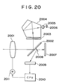
- Figure 20 is a schematic view showing a camera, i.e., a commonly termed single-lens reflex camera.
- Designated at 2001 is an image pick-up optical system for focusing an object image on film 2007 or on focus plate 2004.
- Light image transmitted through image pick-up optical system 2001 is bent by main mirror 2002 to be focused on focus plate 2003, and this image is then led by pentaprism 2004 and eyepiece lens 2005 to a photosensor or to eyes.
- the image is also led by a half mirror section provided on main mirror 2002, and part of light image is bent by sub-mirror 2008 to be led to focus detection unit 2009.
- This focus detection unit 2009 has the photoelectric converter as described before. The detection of focus is done with reference to the peak and bottom values of the output signal as described before.
- CPU 2010 undertakes control for the focusing as noted above.
- main mirror 2002 and sub-mirror 2008 are kicked upwards in the Figure, and a shutter (not shown) provided right in front of film 2007 is operated as desired.
- the maximum/minimum value detection circuit has a monolithic structure located between photoreceiving element and reading circuit, and with this structure the following effects can be obtained.
Landscapes
- Power Engineering (AREA)
- Physics & Mathematics (AREA)
- Engineering & Computer Science (AREA)
- Computer Hardware Design (AREA)
- General Physics & Mathematics (AREA)
- Condensed Matter Physics & Semiconductors (AREA)
- Electromagnetism (AREA)
- Microelectronics & Electronic Packaging (AREA)
- Transforming Light Signals Into Electric Signals (AREA)
- Optical Head (AREA)
- Glass Compositions (AREA)
- Amplifiers (AREA)
- Solid State Image Pick-Up Elements (AREA)
- Photometry And Measurement Of Optical Pulse Characteristics (AREA)
- Light Receiving Elements (AREA)
Applications Claiming Priority (4)
| Application Number | Priority Date | Filing Date | Title |
|---|---|---|---|
| JP2048076A JP2878376B2 (ja) | 1990-02-28 | 1990-02-28 | 光電変換装置 |
| JP48076/90 | 1990-02-28 | ||
| JP4807690 | 1990-02-28 | ||
| EP91301658A EP0444938B1 (fr) | 1990-02-28 | 1991-02-28 | Convertisseur photoélectrique |
Related Parent Applications (2)
| Application Number | Title | Priority Date | Filing Date |
|---|---|---|---|
| EP91301658.0 Division | 1991-02-28 | ||
| EP91301658A Division EP0444938B1 (fr) | 1990-02-28 | 1991-02-28 | Convertisseur photoélectrique |
Publications (3)
| Publication Number | Publication Date |
|---|---|
| EP0710986A2 true EP0710986A2 (fr) | 1996-05-08 |
| EP0710986A3 EP0710986A3 (fr) | 1996-05-29 |
| EP0710986B1 EP0710986B1 (fr) | 2002-06-12 |
Family
ID=12793253
Family Applications (3)
| Application Number | Title | Priority Date | Filing Date |
|---|---|---|---|
| EP91301658A Expired - Lifetime EP0444938B1 (fr) | 1990-02-28 | 1991-02-28 | Convertisseur photoélectrique |
| EP96200019A Expired - Lifetime EP0710986B1 (fr) | 1990-02-28 | 1991-02-28 | Convertisseur photoélectrique |
| EP96200020A Expired - Lifetime EP0713254B1 (fr) | 1990-02-28 | 1991-02-28 | Convertisseur photoélectrique |
Family Applications Before (1)
| Application Number | Title | Priority Date | Filing Date |
|---|---|---|---|
| EP91301658A Expired - Lifetime EP0444938B1 (fr) | 1990-02-28 | 1991-02-28 | Convertisseur photoélectrique |
Family Applications After (1)
| Application Number | Title | Priority Date | Filing Date |
|---|---|---|---|
| EP96200020A Expired - Lifetime EP0713254B1 (fr) | 1990-02-28 | 1991-02-28 | Convertisseur photoélectrique |
Country Status (8)
| Country | Link |
|---|---|
| US (1) | US5591960A (fr) |
| EP (3) | EP0444938B1 (fr) |
| JP (1) | JP2878376B2 (fr) |
| AT (3) | ATE219294T1 (fr) |
| DE (3) | DE69133243T2 (fr) |
| DK (1) | DK0444938T3 (fr) |
| ES (1) | ES2090235T3 (fr) |
| GR (1) | GR3021507T3 (fr) |
Families Citing this family (19)
| Publication number | Priority date | Publication date | Assignee | Title |
|---|---|---|---|---|
| EP0627847B1 (fr) * | 1993-05-28 | 2001-04-11 | Canon Kabushiki Kaisha | Dispositif de conversion photoélectrique |
| JPH09129864A (ja) | 1995-10-30 | 1997-05-16 | Canon Inc | 半導体装置及びそれを用いた半導体回路、相関演算装置、信号処理システム |
| US5848305A (en) * | 1996-01-31 | 1998-12-08 | Canon Kabushiki Kaisha | Circulating shift register and distance measuring device |
| US5838176A (en) * | 1996-07-11 | 1998-11-17 | Foveonics, Inc. | Correlated double sampling circuit |
| US5844265A (en) * | 1996-07-11 | 1998-12-01 | Synaptics, Incorporated | Sense amplifier for high-density imaging array |
| SG70128A1 (en) * | 1997-10-06 | 2000-01-25 | Canon Kk | Method of driving image sensor |
| JP3636579B2 (ja) * | 1997-11-04 | 2005-04-06 | キヤノン株式会社 | 光電変換装置、光電変換装置の駆動方法及びその光電変換装置を有するシステム |
| JPH11307756A (ja) * | 1998-02-20 | 1999-11-05 | Canon Inc | 光電変換装置および放射線読取装置 |
| US6940551B2 (en) | 2000-09-25 | 2005-09-06 | Foveon, Inc. | Active pixel sensor with noise cancellation |
| US6559488B1 (en) * | 2000-10-02 | 2003-05-06 | Stmicroelectronics, Inc. | Integrated photodetector |
| US7104686B2 (en) * | 2001-05-30 | 2006-09-12 | Canon Kabushiki Kaisha | Radiographic apparatus |
| KR20050001077A (ko) * | 2003-06-27 | 2005-01-06 | 삼성전기주식회사 | 수광소자 및 증폭소자가 일체 형성된 반도체 장치 및 그제조방법 |
| US7568628B2 (en) | 2005-03-11 | 2009-08-04 | Hand Held Products, Inc. | Bar code reading device with global electronic shutter control |
| US7611060B2 (en) | 2005-03-11 | 2009-11-03 | Hand Held Products, Inc. | System and method to automatically focus an image reader |
| US7780089B2 (en) | 2005-06-03 | 2010-08-24 | Hand Held Products, Inc. | Digital picture taking optical reader having hybrid monochrome and color image sensor array |
| US7770799B2 (en) | 2005-06-03 | 2010-08-10 | Hand Held Products, Inc. | Optical reader having reduced specular reflection read failures |
| JP5564421B2 (ja) * | 2007-06-21 | 2014-07-30 | ザ・ジョンズ・ホプキンス・ユニバーシティ | バーチャル顕微鏡スライド/デジタル画像をナビゲートするための操作デバイス及びそれに関連する方法。 |
| US10338012B2 (en) * | 2016-03-09 | 2019-07-02 | Toshiba Medical Systems Corporation | Photon counting detector and X-ray computed tomography (CT) apparatus |
| CN111370437B (zh) * | 2020-04-22 | 2023-03-14 | 厦门大学 | 一种基于金属氧化物薄膜晶体管的集成探测基板 |
Citations (6)
| Publication number | Priority date | Publication date | Assignee | Title |
|---|---|---|---|---|
| JPS58127370A (ja) * | 1982-01-25 | 1983-07-29 | Toshiba Corp | 固体撮像装置 |
| US4751559A (en) * | 1985-11-13 | 1988-06-14 | Canon Kabushiki Kaisha | Photoelectric conversion device |
| EP0275217A2 (fr) * | 1987-01-16 | 1988-07-20 | Canon Kabushiki Kaisha | Dispositif de conversion photovoltaique |
| EP0311529A2 (fr) * | 1987-10-09 | 1989-04-12 | Fujitsu Limited | Capteur d'images comportant des régions de stockage de charges |
| JPH01222583A (ja) * | 1988-03-02 | 1989-09-05 | Canon Inc | 光電変換装置並びに該装置の蓄積動作を制御する蓄積制御装置 |
| EP0400754A1 (fr) * | 1989-06-02 | 1990-12-05 | Koninklijke Philips Electronics N.V. | Dispositif semi-conducteur photosensible |
Family Cites Families (6)
| Publication number | Priority date | Publication date | Assignee | Title |
|---|---|---|---|---|
| CA1289242C (fr) * | 1985-11-13 | 1991-09-17 | Shigetoshi Sugawa | Methode et dispositif de conversion photoelectrique de la lumiere en un signal |
| JP2692049B2 (ja) * | 1986-07-10 | 1997-12-17 | キヤノン株式会社 | 焦点検出装置 |
| JPH07120767B2 (ja) * | 1986-09-19 | 1995-12-20 | キヤノン株式会社 | 光電変換装置 |
| JP2526953B2 (ja) * | 1987-12-25 | 1996-08-21 | 株式会社ニコン | 焦点検出装置 |
| NL8801342A (nl) * | 1988-05-25 | 1989-12-18 | Imec Inter Uni Micro Electr | Stralingsopnemer. |
| JPH03100535A (ja) * | 1989-09-13 | 1991-04-25 | Minolta Camera Co Ltd | カメラのピント検出用光電変換装置 |
-
1990
- 1990-02-28 JP JP2048076A patent/JP2878376B2/ja not_active Expired - Fee Related
-
1991
- 1991-02-28 EP EP91301658A patent/EP0444938B1/fr not_active Expired - Lifetime
- 1991-02-28 ES ES91301658T patent/ES2090235T3/es not_active Expired - Lifetime
- 1991-02-28 DE DE69133243T patent/DE69133243T2/de not_active Expired - Fee Related
- 1991-02-28 AT AT96200019T patent/ATE219294T1/de not_active IP Right Cessation
- 1991-02-28 DE DE69133037T patent/DE69133037T2/de not_active Expired - Fee Related
- 1991-02-28 EP EP96200019A patent/EP0710986B1/fr not_active Expired - Lifetime
- 1991-02-28 AT AT91301658T patent/ATE141459T1/de not_active IP Right Cessation
- 1991-02-28 EP EP96200020A patent/EP0713254B1/fr not_active Expired - Lifetime
- 1991-02-28 DK DK91301658.0T patent/DK0444938T3/da active
- 1991-02-28 AT AT96200020T patent/ATE238608T1/de not_active IP Right Cessation
- 1991-02-28 DE DE69121262T patent/DE69121262T2/de not_active Expired - Fee Related
-
1995
- 1995-02-22 US US08/392,619 patent/US5591960A/en not_active Expired - Lifetime
-
1996
- 1996-10-30 GR GR960402876T patent/GR3021507T3/el unknown
Patent Citations (6)
| Publication number | Priority date | Publication date | Assignee | Title |
|---|---|---|---|---|
| JPS58127370A (ja) * | 1982-01-25 | 1983-07-29 | Toshiba Corp | 固体撮像装置 |
| US4751559A (en) * | 1985-11-13 | 1988-06-14 | Canon Kabushiki Kaisha | Photoelectric conversion device |
| EP0275217A2 (fr) * | 1987-01-16 | 1988-07-20 | Canon Kabushiki Kaisha | Dispositif de conversion photovoltaique |
| EP0311529A2 (fr) * | 1987-10-09 | 1989-04-12 | Fujitsu Limited | Capteur d'images comportant des régions de stockage de charges |
| JPH01222583A (ja) * | 1988-03-02 | 1989-09-05 | Canon Inc | 光電変換装置並びに該装置の蓄積動作を制御する蓄積制御装置 |
| EP0400754A1 (fr) * | 1989-06-02 | 1990-12-05 | Koninklijke Philips Electronics N.V. | Dispositif semi-conducteur photosensible |
Non-Patent Citations (3)
| Title |
|---|
| FUJITSU SCIENTIFIC & TECHNICAL JOURNAL, vol. 23, no. 1, 1987 KAWASAKI, JAPAN, pages 1-16, TERUO SAKURAI 'FOUR-CHANNEL OPTOELECTRONIC INTEGRATED CIRCUITS' * |
| PATENT ABSTRACTS OF JAPAN vol. 007 no. 236 (E-205) ,20 October 1983 & JP-A-58 127370 (TOKYO SHIBAURA DENKI KK) 29 July 1983, * |
| PATENT ABSTRACTS OF JAPAN vol. 013 no. 541 (E-854) ,5 December 1989 & JP-A-01 222583 (CANON INC) 5 September 1989, * |
Also Published As
| Publication number | Publication date |
|---|---|
| DE69133037T2 (de) | 2002-11-14 |
| JPH03250983A (ja) | 1991-11-08 |
| ATE141459T1 (de) | 1996-08-15 |
| DE69133037D1 (de) | 2002-07-18 |
| EP0713254A2 (fr) | 1996-05-22 |
| JP2878376B2 (ja) | 1999-04-05 |
| DE69121262D1 (de) | 1996-09-19 |
| DK0444938T3 (da) | 1996-09-02 |
| EP0444938A2 (fr) | 1991-09-04 |
| ES2090235T3 (es) | 1996-10-16 |
| EP0444938B1 (fr) | 1996-08-14 |
| EP0444938A3 (en) | 1992-04-08 |
| ATE238608T1 (de) | 2003-05-15 |
| EP0713254B1 (fr) | 2003-04-23 |
| GR3021507T3 (en) | 1997-01-31 |
| EP0710986A3 (fr) | 1996-05-29 |
| EP0710986B1 (fr) | 2002-06-12 |
| DE69133243T2 (de) | 2004-01-08 |
| EP0713254A3 (fr) | 1996-11-27 |
| US5591960A (en) | 1997-01-07 |
| ATE219294T1 (de) | 2002-06-15 |
| DE69133243D1 (de) | 2003-05-28 |
| DE69121262T2 (de) | 1997-01-09 |
Similar Documents
| Publication | Publication Date | Title |
|---|---|---|
| EP0444938B1 (fr) | Convertisseur photoélectrique | |
| US7889271B2 (en) | AE/AF sensor device with photometry conversion element formed using plural semiconductor regions and automatic focusing photoelectric conversion element formed using plural semiconductor regions | |
| US4862237A (en) | Solid state image sensor | |
| US20110007197A1 (en) | Amplifying solid-state imaging device, and method for driving the same | |
| US20090086063A1 (en) | Solid-state imaging device and imaging apparatus using the same | |
| US7038183B2 (en) | Image sensor device comprising central locking | |
| EP0559138B1 (fr) | Dispostif capteur d'image à l'état solide | |
| JP3278243B2 (ja) | 光電変換装置 | |
| CA1128197A (fr) | Dispositif de visualisation a semiconducteurs | |
| US4148051A (en) | Solid-state imaging device | |
| US11728359B2 (en) | Image sensor having two-colored color filters sharing one photodiode | |
| EP1551061A2 (fr) | Capteur d'images CMOS et méthode pour détecter sa sensibilité couleur | |
| JPH07264485A (ja) | 撮像装置 | |
| JP2839107B2 (ja) | 光電変換装置 | |
| KR950008709B1 (ko) | 고체영상장치 | |
| US5115293A (en) | Solid-state imaging device | |
| JPH07284026A (ja) | 固体撮像装置 | |
| US20220068987A1 (en) | Image sensing device | |
| KR102625261B1 (ko) | 이미지 장치 | |
| EP1406304A2 (fr) | Capteur d'image à l'état solide | |
| JP3950726B2 (ja) | 固体撮像装置及び撮影システム | |
| US20050098797A1 (en) | Photoelectric conversion device and image sensor IC | |
| JPH1022489A (ja) | 固体撮像素子 | |
| JP2555150B2 (ja) | 固体撮像装置 | |
| JPH09275204A (ja) | 固体撮像素子 |
Legal Events
| Date | Code | Title | Description |
|---|---|---|---|
| PUAI | Public reference made under article 153(3) epc to a published international application that has entered the european phase |
Free format text: ORIGINAL CODE: 0009012 |
|
| PUAL | Search report despatched |
Free format text: ORIGINAL CODE: 0009013 |
|
| AC | Divisional application: reference to earlier application |
Ref document number: 444938 Country of ref document: EP |
|
| AK | Designated contracting states |
Kind code of ref document: A2 Designated state(s): AT BE CH DE DK ES FR GB GR IT LI LU NL SE |
|
| AK | Designated contracting states |
Kind code of ref document: A3 Designated state(s): AT BE CH DE DK ES FR GB GR IT LI LU NL SE |
|
| 17P | Request for examination filed |
Effective date: 19961009 |
|
| 17Q | First examination report despatched |
Effective date: 19981023 |
|
| GRAG | Despatch of communication of intention to grant |
Free format text: ORIGINAL CODE: EPIDOS AGRA |
|
| GRAG | Despatch of communication of intention to grant |
Free format text: ORIGINAL CODE: EPIDOS AGRA |
|
| GRAG | Despatch of communication of intention to grant |
Free format text: ORIGINAL CODE: EPIDOS AGRA |
|
| GRAH | Despatch of communication of intention to grant a patent |
Free format text: ORIGINAL CODE: EPIDOS IGRA |
|
| GRAH | Despatch of communication of intention to grant a patent |
Free format text: ORIGINAL CODE: EPIDOS IGRA |
|
| GRAA | (expected) grant |
Free format text: ORIGINAL CODE: 0009210 |
|
| AC | Divisional application: reference to earlier application |
Ref document number: 444938 Country of ref document: EP |
|
| AK | Designated contracting states |
Kind code of ref document: B1 Designated state(s): AT BE CH DE DK ES FR GB GR IT LI LU NL SE |
|
| PG25 | Lapsed in a contracting state [announced via postgrant information from national office to epo] |
Ref country code: NL Free format text: LAPSE BECAUSE OF FAILURE TO SUBMIT A TRANSLATION OF THE DESCRIPTION OR TO PAY THE FEE WITHIN THE PRESCRIBED TIME-LIMIT Effective date: 20020612 Ref country code: LI Free format text: LAPSE BECAUSE OF FAILURE TO SUBMIT A TRANSLATION OF THE DESCRIPTION OR TO PAY THE FEE WITHIN THE PRESCRIBED TIME-LIMIT Effective date: 20020612 Ref country code: IT Free format text: LAPSE BECAUSE OF FAILURE TO SUBMIT A TRANSLATION OF THE DESCRIPTION OR TO PAY THE FEE WITHIN THE PRESCRIBED TIME-LIMIT;WARNING: LAPSES OF ITALIAN PATENTS WITH EFFECTIVE DATE BEFORE 2007 MAY HAVE OCCURRED AT ANY TIME BEFORE 2007. THE CORRECT EFFECTIVE DATE MAY BE DIFFERENT FROM THE ONE RECORDED. Effective date: 20020612 Ref country code: GR Free format text: LAPSE BECAUSE OF FAILURE TO SUBMIT A TRANSLATION OF THE DESCRIPTION OR TO PAY THE FEE WITHIN THE PRESCRIBED TIME-LIMIT Effective date: 20020612 Ref country code: CH Free format text: LAPSE BECAUSE OF FAILURE TO SUBMIT A TRANSLATION OF THE DESCRIPTION OR TO PAY THE FEE WITHIN THE PRESCRIBED TIME-LIMIT Effective date: 20020612 Ref country code: BE Free format text: LAPSE BECAUSE OF FAILURE TO SUBMIT A TRANSLATION OF THE DESCRIPTION OR TO PAY THE FEE WITHIN THE PRESCRIBED TIME-LIMIT Effective date: 20020612 Ref country code: AT Free format text: LAPSE BECAUSE OF FAILURE TO SUBMIT A TRANSLATION OF THE DESCRIPTION OR TO PAY THE FEE WITHIN THE PRESCRIBED TIME-LIMIT Effective date: 20020612 |
|
| REF | Corresponds to: |
Ref document number: 219294 Country of ref document: AT Date of ref document: 20020615 Kind code of ref document: T |
|
| REG | Reference to a national code |
Ref country code: GB Ref legal event code: FG4D |
|
| REG | Reference to a national code |
Ref country code: CH Ref legal event code: EP |
|
| REF | Corresponds to: |
Ref document number: 69133037 Country of ref document: DE Date of ref document: 20020718 |
|
| ET | Fr: translation filed | ||
| ET | Fr: translation filed | ||
| PG25 | Lapsed in a contracting state [announced via postgrant information from national office to epo] |
Ref country code: SE Free format text: LAPSE BECAUSE OF FAILURE TO SUBMIT A TRANSLATION OF THE DESCRIPTION OR TO PAY THE FEE WITHIN THE PRESCRIBED TIME-LIMIT Effective date: 20020912 Ref country code: DK Free format text: LAPSE BECAUSE OF FAILURE TO SUBMIT A TRANSLATION OF THE DESCRIPTION OR TO PAY THE FEE WITHIN THE PRESCRIBED TIME-LIMIT Effective date: 20020912 |
|
| NLV1 | Nl: lapsed or annulled due to failure to fulfill the requirements of art. 29p and 29m of the patents act | ||
| PG25 | Lapsed in a contracting state [announced via postgrant information from national office to epo] |
Ref country code: ES Free format text: LAPSE BECAUSE OF FAILURE TO SUBMIT A TRANSLATION OF THE DESCRIPTION OR TO PAY THE FEE WITHIN THE PRESCRIBED TIME-LIMIT Effective date: 20021220 |
|
| REG | Reference to a national code |
Ref country code: CH Ref legal event code: PL |
|
| PG25 | Lapsed in a contracting state [announced via postgrant information from national office to epo] |
Ref country code: LU Free format text: LAPSE BECAUSE OF NON-PAYMENT OF DUE FEES Effective date: 20030228 |
|
| PLBE | No opposition filed within time limit |
Free format text: ORIGINAL CODE: 0009261 |
|
| STAA | Information on the status of an ep patent application or granted ep patent |
Free format text: STATUS: NO OPPOSITION FILED WITHIN TIME LIMIT |
|
| 26N | No opposition filed |
Effective date: 20030313 |
|
| PGFP | Annual fee paid to national office [announced via postgrant information from national office to epo] |
Ref country code: DE Payment date: 20090228 Year of fee payment: 19 |
|
| PGFP | Annual fee paid to national office [announced via postgrant information from national office to epo] |
Ref country code: GB Payment date: 20090218 Year of fee payment: 19 |
|
| PGFP | Annual fee paid to national office [announced via postgrant information from national office to epo] |
Ref country code: FR Payment date: 20090223 Year of fee payment: 19 |
|
| GBPC | Gb: european patent ceased through non-payment of renewal fee |
Effective date: 20100228 |
|
| REG | Reference to a national code |
Ref country code: FR Ref legal event code: ST Effective date: 20101029 |
|
| PG25 | Lapsed in a contracting state [announced via postgrant information from national office to epo] |
Ref country code: FR Free format text: LAPSE BECAUSE OF NON-PAYMENT OF DUE FEES Effective date: 20100301 |
|
| PG25 | Lapsed in a contracting state [announced via postgrant information from national office to epo] |
Ref country code: DE Free format text: LAPSE BECAUSE OF NON-PAYMENT OF DUE FEES Effective date: 20100901 |
|
| PG25 | Lapsed in a contracting state [announced via postgrant information from national office to epo] |
Ref country code: GB Free format text: LAPSE BECAUSE OF NON-PAYMENT OF DUE FEES Effective date: 20100228 |