EP0708481A2 - Verbesserte thermische Höcker für monolithische integrierte Schaltungen höherer Leistung vom Flipchip-Typ und Herstellungsverfahren - Google Patents
Verbesserte thermische Höcker für monolithische integrierte Schaltungen höherer Leistung vom Flipchip-Typ und Herstellungsverfahren Download PDFInfo
- Publication number
- EP0708481A2 EP0708481A2 EP95115956A EP95115956A EP0708481A2 EP 0708481 A2 EP0708481 A2 EP 0708481A2 EP 95115956 A EP95115956 A EP 95115956A EP 95115956 A EP95115956 A EP 95115956A EP 0708481 A2 EP0708481 A2 EP 0708481A2
- Authority
- EP
- European Patent Office
- Prior art keywords
- mmic
- photoresist
- bump
- layer
- pads
- Prior art date
- Legal status (The legal status is an assumption and is not a legal conclusion. Google has not performed a legal analysis and makes no representation as to the accuracy of the status listed.)
- Withdrawn
Links
Images


Classifications
-
- H10W76/12—
-
- H10W72/20—
-
- H10W20/483—
-
- H10W44/20—
-
- H10W72/07236—
-
- H10W72/251—
-
- H10W72/252—
-
- H10W72/952—
Definitions
- High thermal resistance paths are critical for optimum performance of high power or high efficiency electronic microwave devices such as field-effect transistors (FETs), high electron mobility transistors (HEMTs), and heterojunction bipolar transistors (HBTs). All of these devices generate energy in the form of heat due to resistive parasitics and losses in the devices themselves. As the temperature of the device increases, the radio frequency (RF) performance degrades, and the device may even experience catastrophic failure due to self-heating. Consequently, heat must be taken from the device's active area in which the heat is generated and transferred elsewhere, such as to a module substrate.
- RF radio frequency
- Fig. 1 shows a conventional flip-chip mounted microwave monolithic integrated circuit (MMIC) assembly 30.
- the assembly includes a MMIC chip 32 which is flip-chip mounted on a host substrate 34.
- the chip 32 has a substrate-facing surface 36, whereas the substrate 34 has a chip-facing surface 38.
- the chip 32 is typically formed of 635 micrometer thick GaAs, whereas the substrate 34 is typically formed of beryllium oxide or alumina and may have any suitable thickness.
- Active electronic devices 40 are formed on the substrate-facing surface 36 of the chip 32.
- the devices 40 may be similar or different, and formed by any suitable process such as ion implantation, epitaxy, etc.
- the devices 40 may be, for example, FETs, HEMTs, or HBTs, and have active areas 42 in which heat is generated during operation.
- Thermally conductive contacts or pads 44 are formed on the surface 36 in close proximity to the active areas 42, respectively.
- the pads 44 may also be electrically conductive, and constitute electrical contact pads for elements of the devices 40. For example, where the devices 40 are FETs connected in a common-source configuration, the pads 44 may be source contact pads of the devices 40.
- the chip 32 is flip-chip mounted on the substrate 34 using a conventional reflow or other soldering process by which the bumps 50 are soldered and thereby electrically and thermally connected to metal pads (not shown) attached to the substrate, and the bumps 52 are similarly soldered to the ground plane portions 54, respectively.
- the bumps 50 conduct heat generated at the active areas 42 of the devices 40 to the substrate 34, thereby removing the heat from the devices 40 and the surrounding areas of the chip 32.
- the active area of the MMIC may include a number of source pads, gate pads, drain pads, and electrically conductive air bridges. Air bridges may extend over the gate pads and drain pads, with the source pads interposed in between the air bridges.
- the thermally conductive bump may also be electrically conductive. The bump may be in electrical contact with the source pads and the air bridges, with the gate pads and drain pads being separated from the air bridges by free air spaces. The gate pads and drain pads may be free from electrical contact with the bump.
- the host substrate may serve as a common ground to the source pads.
- a multi-layer, multi-exposure method of manufacturing an improved thermally conductive, "T"-shaped thermal bump may have several steps.
- a plating membrane is formed on the connection pad of the MMIC.
- a first layer of negative photoresist is applied to the surface of the plating membrane.
- the first layer of negative photoresist is exposed with the first masked pattern of light, in which a first rectangular area of photoresist is left unexposed.
- a second layer of negative photoresist is applied on top of the first layer of photoresist.
- the second layer of negative photoresist is exposed to a second masked pattern of light which leaves a second rectangular unexposed portion of negative photoresist juxtaposed above the first rectangular unexposed portion.
- a third layer of negative photoresist is applied on top of the second layer of photoresist.
- the third layer of photoresist is exposed with a third masked pattern of light leaving a third unexposed portion of negative photoresist which is wider than the first and second unexposed portions of photoresist.
- a variety of shapes may be constructed.
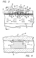
- FIG. 3 is a detailed view of the active area of a specific flip-chip MMIC assembly 60 in which the devices 40 shown in FIG. 1 are embodied by power field-effect transistors 62. Like elements are designated by the same reference numerals used in Fig. 1.
- Each transistor 62 includes a source 62A, drain 62B and channel 62C.
- the transistors 62 may be formed using conventional procedures such as ion implantation, epitaxy, or any other suitable process.
- the transistors 62 generate maximum heat in active areas 72 constituted mainly by the portions of the channels 62C between the gate pads 68 and the drains 62B. These transistors are mounted on a typically ceramic substrate 34 by means of generally trapezoidal thermal bumps 51 each of which interconnect several adjacent transistors to substrate 34. As illustrated by arrows 74 and 76, heat generated during operation of the transistors 62 flows from the active areas 72 through a relatively short portion of the body of the chip 32, the source pads 64, the air bridge 70, and the bumps 51 (Figs. 3 and 4) to the substrate 34.
- the source pads 64 are electrically interconnected by the air bridge 70, which is in turn electrically connected to the substrate.
- the bumps 50 therefore provide both heat sinking and electrical grounding functions.
- the bumps 51 are typically soldered to host substrate 34 with lead-indium solder using known soldering techniques.
- the present invention takes advantage of the fact that the thermal resistance of the substrate is a function of the cross-sectional area, or footprint, of the plated metal bumps at the substrate. That is, the amount of heat that is dissipated into the substrate increases as the cross-sectional area of the plated bumps at the substrate also increases.
- the thermal bumps of the present invention having a limited area at the point of heat generation, are configured to have a larger heat transmitting area where they contact the high thermal resistance substrate.
- a "T" shaped bump having narrow portion dimensions of 130 by 592 micrometers and thicker portion dimensions of 208 by 592 micrometers reduced the peak temperature rise to only 68 degrees centigrade. It may be noted that the better-performing "T" shape bump had a cross-sectional area that was approximately 1.6 times greater at the substrate than at the MMIC.
- a first layer of negative photoresist 84 is then applied to the surface of the plating membrane 80.
- Methods of applying negative photoresist are well known in the art.
- the negative photoresist may be supplied in dry sheet form.
- the layers of photoresist 84 and 90 are then developed with a photoresist developer, and the unexposed "T” areas are removed, thereby leaving a substantially "T"-shaped via 94, which is also known as a void, where the unexposed "T” of photoresist had been.
- Methods of developing and removing photoresist are well-known in the art.
Landscapes
- Cooling Or The Like Of Semiconductors Or Solid State Devices (AREA)
- Internal Circuitry In Semiconductor Integrated Circuit Devices (AREA)
- Wire Bonding (AREA)
Applications Claiming Priority (2)
| Application Number | Priority Date | Filing Date | Title |
|---|---|---|---|
| US32629294A | 1994-10-20 | 1994-10-20 | |
| US326292 | 1994-10-20 |
Publications (2)
| Publication Number | Publication Date |
|---|---|
| EP0708481A2 true EP0708481A2 (de) | 1996-04-24 |
| EP0708481A3 EP0708481A3 (de) | 1997-04-02 |
Family
ID=23271613
Family Applications (1)
| Application Number | Title | Priority Date | Filing Date |
|---|---|---|---|
| EP95115956A Withdrawn EP0708481A3 (de) | 1994-10-20 | 1995-10-10 | Verbesserte thermische Höcker für monolithische integrierte Schaltungen höherer Leistung vom Flipchip-Typ und Herstellungsverfahren |
Country Status (3)
| Country | Link |
|---|---|
| US (2) | US5616517A (de) |
| EP (1) | EP0708481A3 (de) |
| KR (1) | KR100211269B1 (de) |
Cited By (1)
| Publication number | Priority date | Publication date | Assignee | Title |
|---|---|---|---|---|
| WO2001056081A1 (en) * | 2000-01-27 | 2001-08-02 | Bookham Technology Plc | Flip-chip bonding arrangement |
Families Citing this family (21)
| Publication number | Priority date | Publication date | Assignee | Title |
|---|---|---|---|---|
| US6227436B1 (en) | 1990-02-19 | 2001-05-08 | Hitachi, Ltd. | Method of fabricating an electronic circuit device and apparatus for performing the method |
| US6471115B1 (en) | 1990-02-19 | 2002-10-29 | Hitachi, Ltd. | Process for manufacturing electronic circuit devices |
| JPH1070153A (ja) * | 1996-08-26 | 1998-03-10 | Hitachi Ltd | 電子部品の接続方法 |
| KR19990040212A (ko) * | 1997-11-17 | 1999-06-05 | 김영환 | 이동통신 시스템의 운용보드 기능 시험 장치 |
| US5904555A (en) * | 1998-02-02 | 1999-05-18 | Motorola, Inc. | Method for packaging a semiconductor device |
| JP3609935B2 (ja) * | 1998-03-10 | 2005-01-12 | シャープ株式会社 | 高周波半導体装置 |
| US6222276B1 (en) | 1998-04-07 | 2001-04-24 | International Business Machines Corporation | Through-chip conductors for low inductance chip-to-chip integration and off-chip connections |
| US5990757A (en) * | 1998-06-05 | 1999-11-23 | Raytheon Company | Gallium arsenide monolithic microwave integrated circuits employing thermally bumped devices |
| US6081037A (en) * | 1998-06-22 | 2000-06-27 | Motorola, Inc. | Semiconductor component having a semiconductor chip mounted to a chip mount |
| US6465157B1 (en) * | 2000-01-31 | 2002-10-15 | Chartered Semiconductor Manufacturing Ltd | Dual layer pattern formation method for dual damascene interconnect |
| US6507110B1 (en) | 2000-03-08 | 2003-01-14 | Teledyne Technologies Incorporated | Microwave device and method for making same |
| US6602775B1 (en) * | 2001-08-16 | 2003-08-05 | Taiwan Semiconductor Manufacturing Company | Method to improve reliability for flip-chip device for limiting pad design |
| US6486054B1 (en) * | 2002-01-28 | 2002-11-26 | Taiwan Semiconductor Manufacturing Company | Method to achieve robust solder bump height |
| US6933603B2 (en) * | 2002-07-11 | 2005-08-23 | Teledyne Technologies Incorporated | Multi-substrate layer semiconductor packages and method for making same |
| TWI222732B (en) * | 2003-07-18 | 2004-10-21 | Advanced Semiconductor Eng | Formation method for conductive bump |
| US7656236B2 (en) * | 2007-05-15 | 2010-02-02 | Teledyne Wireless, Llc | Noise canceling technique for frequency synthesizer |
| US8179045B2 (en) * | 2008-04-22 | 2012-05-15 | Teledyne Wireless, Llc | Slow wave structure having offset projections comprised of a metal-dielectric composite stack |
| US8102038B2 (en) * | 2009-09-18 | 2012-01-24 | Texas Instruments Incorporated | Semiconductor chip attach configuration having improved thermal characteristics |
| JP5736716B2 (ja) * | 2010-10-15 | 2015-06-17 | 富士通株式会社 | 電子装置及びその製造方法、送受信装置 |
| US9202660B2 (en) | 2013-03-13 | 2015-12-01 | Teledyne Wireless, Llc | Asymmetrical slow wave structures to eliminate backward wave oscillations in wideband traveling wave tubes |
| KR102254104B1 (ko) | 2014-09-29 | 2021-05-20 | 삼성전자주식회사 | 반도체 패키지 |
Family Cites Families (29)
| Publication number | Priority date | Publication date | Assignee | Title |
|---|---|---|---|---|
| US4283483A (en) * | 1979-07-19 | 1981-08-11 | Hughes Aircraft Company | Process for forming semiconductor devices using electron-sensitive resist patterns with controlled line profiles |
| US4845542A (en) * | 1987-03-19 | 1989-07-04 | Unisys Corporation | Interconnect for layered integrated circuit assembly |
| US4917466A (en) * | 1987-08-13 | 1990-04-17 | Shin-Etsu Polymer Co., Ltd. | Method for electrically connecting IC chips, a resinous bump-forming composition used therein and a liquid-crystal display unit electrically connected thereby |
| US4912545A (en) * | 1987-09-16 | 1990-03-27 | Irvine Sensors Corporation | Bonding of aligned conductive bumps on adjacent surfaces |
| US4959705A (en) * | 1988-10-17 | 1990-09-25 | Ford Microelectronics, Inc. | Three metal personalization of application specific monolithic microwave integrated circuit |
| US4959326A (en) * | 1988-12-22 | 1990-09-25 | Siemens Aktiengesellschaft | Fabricating T-gate MESFETS employing double exposure, double develop techniques |
| US5139968A (en) * | 1989-03-03 | 1992-08-18 | Mitsubishi Denki Kabushiki Kaisha | Method of producing a t-shaped gate electrode |
| JP2550412B2 (ja) * | 1989-05-15 | 1996-11-06 | ローム株式会社 | 電界効果トランジスタの製造方法 |
| GB2233494A (en) * | 1989-06-26 | 1991-01-09 | Philips Nv | Providing an electrode on a semiconductor device |
| JPH03174731A (ja) * | 1989-09-14 | 1991-07-29 | Fuji Electric Co Ltd | 集積回路装置用バンプ電極およびその製造方法 |
| US5168329A (en) * | 1989-11-06 | 1992-12-01 | Sumitomo Electric Industries, Ltd. | Microwave semiconductor device capable of controlling a threshold voltage |
| JPH03201701A (ja) * | 1989-12-28 | 1991-09-03 | Sharp Corp | マイクロ波装置 |
| US5319237A (en) * | 1990-03-09 | 1994-06-07 | Thomson Composants Microondes | Power semiconductor component |
| US5202288A (en) * | 1990-06-01 | 1993-04-13 | Robert Bosch Gmbh | Method of manufacturing an electronic circuit component incorporating a heat sink |
| JPH04225542A (ja) * | 1990-12-27 | 1992-08-14 | Tanaka Denshi Kogyo Kk | 半導体装置 |
| JPH04260338A (ja) * | 1991-02-14 | 1992-09-16 | Mitsubishi Electric Corp | 半導体装置の製造方法 |
| US5349239A (en) * | 1991-07-04 | 1994-09-20 | Sharp Kabushiki Kaisha | Vertical type construction transistor |
| JP2723405B2 (ja) * | 1991-11-12 | 1998-03-09 | 松下電器産業株式会社 | 微細電極の形成方法 |
| US5350947A (en) * | 1991-11-12 | 1994-09-27 | Nec Corporation | Film carrier semiconductor device |
| US5334542A (en) * | 1991-11-27 | 1994-08-02 | Oki Electric Industry Co., Ltd. | Method of forming T-shaped electrode |
| JP3322432B2 (ja) * | 1992-03-11 | 2002-09-09 | 株式会社東芝 | 多層配線基板 |
| US5506755A (en) * | 1992-03-11 | 1996-04-09 | Kabushiki Kaisha Toshiba | Multi-layer substrate |
| US5246880A (en) * | 1992-04-27 | 1993-09-21 | Eastman Kodak Company | Method for creating substrate electrodes for flip chip and other applications |
| US5304511A (en) * | 1992-09-29 | 1994-04-19 | Mitsubishi Denki Kabushiki Kaisha | Production method of T-shaped gate electrode in semiconductor device |
| EP0598555A1 (de) * | 1992-11-17 | 1994-05-25 | AT&T Corp. | Herstellungsverfahren für Eingangs-/Ausgangshöcker |
| JP3119957B2 (ja) * | 1992-11-30 | 2000-12-25 | 株式会社東芝 | 半導体装置の製造方法 |
| US5376584A (en) * | 1992-12-31 | 1994-12-27 | International Business Machines Corporation | Process of making pad structure for solder ball limiting metallurgy having reduced edge stress |
| US5352926A (en) * | 1993-01-04 | 1994-10-04 | Motorola, Inc. | Flip chip package and method of making |
| US5424693A (en) * | 1993-01-13 | 1995-06-13 | Industrial Technology Research Institute | Surface mountable microwave IC package |
-
1995
- 1995-10-10 EP EP95115956A patent/EP0708481A3/de not_active Withdrawn
- 1995-10-19 KR KR1019950036105A patent/KR100211269B1/ko not_active Expired - Fee Related
-
1996
- 1996-03-15 US US08/616,414 patent/US5616517A/en not_active Expired - Lifetime
- 1996-12-20 US US08/771,458 patent/US5708283A/en not_active Expired - Lifetime
Non-Patent Citations (1)
| Title |
|---|
| None |
Cited By (1)
| Publication number | Priority date | Publication date | Assignee | Title |
|---|---|---|---|---|
| WO2001056081A1 (en) * | 2000-01-27 | 2001-08-02 | Bookham Technology Plc | Flip-chip bonding arrangement |
Also Published As
| Publication number | Publication date |
|---|---|
| KR100211269B1 (ko) | 1999-07-15 |
| KR960015870A (ko) | 1996-05-22 |
| US5708283A (en) | 1998-01-13 |
| US5616517A (en) | 1997-04-01 |
| EP0708481A3 (de) | 1997-04-02 |
Similar Documents
| Publication | Publication Date | Title |
|---|---|---|
| US5708283A (en) | Flip chip high power monolithic integrated circuit thermal bumps | |
| KR100367936B1 (ko) | 적층체를구비한고주파집적회로장치 | |
| US3903590A (en) | Multiple chip integrated circuits and method of manufacturing the same | |
| US5532512A (en) | Direct stacked and flip chip power semiconductor device structures | |
| US4376287A (en) | Microwave power circuit with an active device mounted on a heat dissipating substrate | |
| US7005734B2 (en) | Double-sided cooling isolated packaged power semiconductor device | |
| KR20010071766A (ko) | 반도체 소자용 캡슐 | |
| US20050077599A1 (en) | Package type semiconductor device | |
| EP0637078A1 (de) | Eine Halbleiteranordnung mit verbesserter Wärmezerstreuung | |
| US7723837B2 (en) | Semiconductor device | |
| US9721909B1 (en) | Hybrid microwave integrated circuit | |
| KR100383418B1 (ko) | 반도체 장치 및 그 제조 방법 | |
| US4736273A (en) | Power semiconductor device for surface mounting | |
| JP4480818B2 (ja) | 半導体装置 | |
| KR100503531B1 (ko) | 반도체디바이스 | |
| US9000496B1 (en) | Source bridge for cooling and/or external connection | |
| US20020171153A1 (en) | Semiconductor device including semiconductor bare chip mounted by flip-chip bonding, and board member with thin-film structure capacitor for semiconductor bare chip mounted by flip-chip bonding | |
| US7193297B2 (en) | Semiconductor device, method for manufacturing the same, circuit substrate and electronic device | |
| KR20230046470A (ko) | 파워모듈용 세라믹 기판, 그 제조방법 및 이를 구비한 파워모듈 | |
| JPH09213730A (ja) | 高周波用モジュール基板およびそれを用いた高周波電力増幅モジュール | |
| JPH08274228A (ja) | 半導体搭載基板、電力用半導体装置及び電子回路装置 | |
| KR20020010489A (ko) | 집적 회로 패키지 | |
| JPH0613487A (ja) | マルチチップモジュール | |
| US11521928B2 (en) | Reducing stress cracks in substrates | |
| JPS63261738A (ja) | 集積回路担持用電気的構成要素 |
Legal Events
| Date | Code | Title | Description |
|---|---|---|---|
| PUAI | Public reference made under article 153(3) epc to a published international application that has entered the european phase |
Free format text: ORIGINAL CODE: 0009012 |
|
| AK | Designated contracting states |
Kind code of ref document: A2 Designated state(s): DE FR GB IT |
|
| PUAL | Search report despatched |
Free format text: ORIGINAL CODE: 0009013 |
|
| AK | Designated contracting states |
Kind code of ref document: A3 Designated state(s): DE FR GB IT |
|
| STAA | Information on the status of an ep patent application or granted ep patent |
Free format text: STATUS: THE APPLICATION IS DEEMED TO BE WITHDRAWN |
|
| 18D | Application deemed to be withdrawn |
Effective date: 19971003 |