EP0706100A1 - Zeitintervalmessvorrichtung - Google Patents
Zeitintervalmessvorrichtung Download PDFInfo
- Publication number
- EP0706100A1 EP0706100A1 EP95402202A EP95402202A EP0706100A1 EP 0706100 A1 EP0706100 A1 EP 0706100A1 EP 95402202 A EP95402202 A EP 95402202A EP 95402202 A EP95402202 A EP 95402202A EP 0706100 A1 EP0706100 A1 EP 0706100A1
- Authority
- EP
- European Patent Office
- Prior art keywords
- circuit
- clock
- signal
- hand
- flop
- Prior art date
- Legal status (The legal status is an assumption and is not a legal conclusion. Google has not performed a legal analysis and makes no representation as to the accuracy of the status listed.)
- Granted
Links
Images


Classifications
-
- G—PHYSICS
- G04—HOROLOGY
- G04F—TIME-INTERVAL MEASURING
- G04F10/00—Apparatus for measuring unknown time intervals by electric means
- G04F10/04—Apparatus for measuring unknown time intervals by electric means by counting pulses or half-cycles of an ac
-
- G—PHYSICS
- G04—HOROLOGY
- G04F—TIME-INTERVAL MEASURING
- G04F10/00—Apparatus for measuring unknown time intervals by electric means
- G04F10/10—Apparatus for measuring unknown time intervals by electric means by measuring electric or magnetic quantities changing in proportion to time
Definitions
- the present invention relates to a device for measuring the duration of a time interval.
- the field of the invention is that of chronometry, of the precise temporal measurement of a period of time, short or infinitely long, between a start signal and an end of measurement signal.
- the present invention aims to solve these problems.
- start (D) and end (F) signals can be completely asynchronous from the clock. This is interesting for applications in the field of telemetry of the "time of flight" type, in which (D) and (F) are given by the departure of a light pulse and by the reception of the pulse reflected on an object. , these two signals (D) and (F) possibly being asynchronous with respect to the clock.
- the digital circuit is provided with a second clock, the pulses of which are offset from those of the first clock, the digital circuit also counts the number of pulses of the second clock which are followed by an entire period and which are between the start (D) and end (F) signal, the analog circuit determines on the one hand the time separating the signal (D) and the start of the first pulse of the second clock which begins after (D) and, on the other hand, the time separating the end signal (F) from the end of the last period of the second clock which ends before (F), and this circuit analog is able to convert the analog data obtained into digital data and the device also comprises means capable of determining which of the counts made on one of the two clocks (H1, H2) is to be taken into account, so as to solve to This ambiguity could lead to an error in counting a clock period.
- the coarse part of the time interval is measured digitally, and the fine part analogically.
- the parameters thus acquired are then combined to obtain the result.
- the time measurement is thus obtained by associating a digital quantity in the form of a number of clock periods counted, and analog quantities obtained by conversion of time into voltage amplitudes.
- t1 and t2 are then digitized, which gives two corresponding values T1 and T2.
- a device for implementing the invention is shown in FIG. 2.
- a clock H delivers pulses of period T on one of the inputs of an AND gate, designated by the reference 2.
- This clock H can be produced from a quartz oscillator, operating for example at a frequency of 200 MHz.
- the other input of the AND gate receives a signal from the output Q of a flip-flop RS designated by the reference 4, on the input S from which the start signal D is sent, while the input R is driven by the end signal F.
- the assembly constituted by the AND gate, the flip-flop 4 and the clock H constitutes a digital measurement circuit making it possible to obtain a rough value of the time interval to be measured. This value is equal to nT where n is the number of clock periods T elapsed between the start signal D and the end signal F. It is counted in a counter 3.
- a division of the frequency of the signals of the clock H is carried out by a divider 6, constituted for example by a rocker, the output of this divider supplying a ramp generator 8.
- This generator can be produced by the load and the constant current discharge of a capacitor. The period and the slope of these ramps are very well defined.
- the output of the ramp generator 8 is sent to a fast analog-digital converter 10 (for example of the flash or fast sampler + converter type), another input of which receives a signal coming for example from a flip-flop 12, controlled by the signals D and F at the start and end of the period to be measured.
- the converter 10 takes the information on the amplitude of the ramp at the instants of start D and of end F of the time interval to be measured, as well as the information relating to the parity of the ramp at these instants, that is to say, its ascending or descending character.
- This converter provides information on the values T1 and T2. This information is stored in a memory 13.
- the rough information relating to nT and the “fine” information relating to the intervals T1 and T2 are sent to a processing circuit 14 which calculates the duration t v of the time interval to be measured.
- This device makes it possible to obtain good accuracy, since it makes it possible to dispense with any synchronization of the start signals D and end signals F of measurement with respect to the clock H of the chronometer; it also overcomes the limited capacity of the chronometer to determine a small and a very large time difference, which can vary from a few picoseconds to infinity, due to its frequency which is fixed.
- This device also makes it possible to determine large time intervals with constant precision, whatever the duration of this time interval. This is not true in the case of devices for measuring the duration of a time interval according to the prior art, in particular in the case of the device described in French patent application No. 93 08145 of July 2, 1993. Indeed, this latter device involves, at the start of measurement of the time interval, the discharge of a capacitor, and at the end of measurement of the time interval the charge of the same capacitor; however, the charge measured immediately after the arrival of the signal D can vary before the final part of the time interval to be measured is reached, just before the end signal F, and this all the more so since l The time interval to be measured is important. In the device according to the present invention, this problem is avoided by using recurrent ramps.
- this type of device can be easily integrated to make a compact circuit.
- a particular embodiment of the invention makes it possible to take account of the problems linked to the situations of ambiguity on the starting signal D and on the arrival signal F. These problems arise when one or the other of these signals , occur simultaneously with a rising or falling edge of the clock signals.
- the counter of the digital part of the device part which determines the rough measurement of the time interval, can then count an additional clock pulse, which should not have been counted.
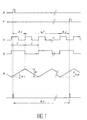
- a clock H1 delivers signals of period T.
- a divider makes it possible to generate signals S1, of period 2T, synchronized with the signals of the clock H1. It is thus possible to generate rising and falling ramps R1, of amplitude A.
- a delay device makes it possible to generate a second clock signal H2, from the signal H1, the signals H2 being offset by T / 2 relative to the signals from H1.
- a falling edge of a slot of H2 corresponds to a rising edge of a slot of H1, as can be seen in FIG. 3.
- This clock signal H2 makes it possible to generate, in the same way as it has been explained above for the clock H1, a signal S2 of period 2T, which will itself control a ramp R2 of the same amplitude A as the ramp R1.
- the two ramps R1 and R2 are sampled simultaneously. If for example there is ambiguity between D and H1, that is to say if the signal D is superimposed on a rising edge of a slot of H1, there cannot be simultaneously ambiguity between the signal D and the signals generated by H2, due to the offset of a half-period between the two channels.
- the valid clock to determine the measurement of t1 is the clock H2 and the value to be taken into account is that measured on the R2 ramp.
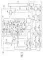
- a first counter 25 receives on its CE authorization input a counting order coming from a flip-flop 23 and on its input C the clock signals H1. Data from the first counter 25 are transmitted to a processing circuit 22 via a routing circuit 36 controlled by an OR circuit 32.
- the D flip-flops 26 and 30 receive the D and F signals via an OR 40, 41 function on their D input.
- the flip-flop 23, which delivers the CE authorization signal, is also controlled by the D and F signals both delayed by an amount close to 3 propagation times in gates by devices 19, 42 which consist for example of delays in logic gates.
- the first AND circuit 27 performs the AND function of the output of the flip-flop 26 and of the clock H2; the signals of the latter are obtained from H1 and a delay circuit 18, constituted for example by propagation times in gates.
- a second counter 29 receives on its CE authorization input a counting order coming from the flip-flop 23.
- the data from this counter 29 is transmitted to the processing circuit 22 via the circuit 36.
- the second flip-flop type D 30 works as described above.
- the second AND circuit 31 performs the AND function between the output of circuit 30 and the clock H1.
- the output of the circuit 32 controls the operation of the routing circuit 36 to obtain the reading of the counter 25 or 29, of which the associated D type flip-flop (26 or 30) did not switch first. It detects the first of the flip-flops 26 or 30 which has switched over and it authorizes the reading of the counter whose flip-flop has not changed state.
- circuits 44, 45 and 46, 47 respectively for the first and second counters. Circuits 44 and 46 are AND circuits, circuits 45 and 47 are time formatting.
- a flip-flop 33 receives on its SET input the output of an OR circuit 34 whose inputs correspond to the signals D and F delayed by circuits 42 and 19.
- the flip-flop 33 receives on its other input the outputs of two doors AND 27, 31.
- This flip-flop 33 controls an input of an analog-digital converter 50 and an input of an analog-digital converter 52. Another input of each of these converters 50, 52 is connected to the clock H1 (respectively H2) by l 'through a flip-flop 51 (respectively 53) which makes it possible to generate a signal S1 respectively S2 of period 2T, and of a ramp generator 55 (respectively 57) for generating a ramp R1 (respectively R2). Downstream of the analog-digital converters, there are two memories 60, 62 and a switching circuit 56 controlled by the circuit 32.
Applications Claiming Priority (2)
| Application Number | Priority Date | Filing Date | Title |
|---|---|---|---|
| FR9411848A FR2725326B1 (fr) | 1994-10-04 | 1994-10-04 | Dispositif de mesure de la duree d'un intervalle de temps |
| FR9411848 | 1994-10-04 |
Publications (2)
| Publication Number | Publication Date |
|---|---|
| EP0706100A1 true EP0706100A1 (de) | 1996-04-10 |
| EP0706100B1 EP0706100B1 (de) | 1998-08-12 |
Family
ID=9467553
Family Applications (1)
| Application Number | Title | Priority Date | Filing Date |
|---|---|---|---|
| EP95402202A Expired - Lifetime EP0706100B1 (de) | 1994-10-04 | 1995-10-02 | Zeitintervalmessvorrichtung |
Country Status (4)
| Country | Link |
|---|---|
| US (1) | US5717659A (de) |
| EP (1) | EP0706100B1 (de) |
| DE (1) | DE69504000T2 (de) |
| FR (1) | FR2725326B1 (de) |
Cited By (1)
| Publication number | Priority date | Publication date | Assignee | Title |
|---|---|---|---|---|
| CN110737189A (zh) * | 2019-11-05 | 2020-01-31 | 中国电子科技集团公司第四十四研究所 | 脉冲激光间隔测量电路 |
Families Citing this family (3)
| Publication number | Priority date | Publication date | Assignee | Title |
|---|---|---|---|---|
| JP3451576B2 (ja) | 1996-09-20 | 2003-09-29 | 株式会社日立製作所 | 情報処理システム |
| US7843771B2 (en) * | 2007-12-14 | 2010-11-30 | Guide Technology, Inc. | High resolution time interpolator |
| CN112506031B (zh) * | 2020-11-30 | 2021-09-21 | 中国计量科学研究院 | 一种激光干涉条纹信号的高精度时间间隔测量系统 |
Citations (3)
| Publication number | Priority date | Publication date | Assignee | Title |
|---|---|---|---|---|
| DE2422727A1 (de) * | 1973-05-11 | 1974-12-05 | Suwa Seikosha Kk | Elektronische uhr |
| US4912734A (en) * | 1989-02-14 | 1990-03-27 | Ail Systems, Inc. | High resolution event occurrance time counter |
| US5200933A (en) * | 1992-05-28 | 1993-04-06 | The United States Of America As Represented By The United States Department Of Energy | High resolution data acquisition |
Family Cites Families (3)
| Publication number | Priority date | Publication date | Assignee | Title |
|---|---|---|---|---|
| JP2568145Y2 (ja) * | 1992-08-14 | 1998-04-08 | 株式会社アドバンテスト | 信号時間差測定装置 |
| FR2707814B1 (fr) * | 1993-07-02 | 1995-09-01 | Commissariat Energie Atomique | Dispositif de mesure de la durée d'un intervalle de temps. |
| US5325340A (en) * | 1993-07-29 | 1994-06-28 | Ramsey Alexander W | Pacing device |
-
1994
- 1994-10-04 FR FR9411848A patent/FR2725326B1/fr not_active Expired - Fee Related
-
1995
- 1995-09-21 US US08/531,377 patent/US5717659A/en not_active Expired - Fee Related
- 1995-10-02 DE DE69504000T patent/DE69504000T2/de not_active Expired - Fee Related
- 1995-10-02 EP EP95402202A patent/EP0706100B1/de not_active Expired - Lifetime
Patent Citations (3)
| Publication number | Priority date | Publication date | Assignee | Title |
|---|---|---|---|---|
| DE2422727A1 (de) * | 1973-05-11 | 1974-12-05 | Suwa Seikosha Kk | Elektronische uhr |
| US4912734A (en) * | 1989-02-14 | 1990-03-27 | Ail Systems, Inc. | High resolution event occurrance time counter |
| US5200933A (en) * | 1992-05-28 | 1993-04-06 | The United States Of America As Represented By The United States Department Of Energy | High resolution data acquisition |
Cited By (1)
| Publication number | Priority date | Publication date | Assignee | Title |
|---|---|---|---|---|
| CN110737189A (zh) * | 2019-11-05 | 2020-01-31 | 中国电子科技集团公司第四十四研究所 | 脉冲激光间隔测量电路 |
Also Published As
| Publication number | Publication date |
|---|---|
| FR2725326B1 (fr) | 1996-10-25 |
| FR2725326A1 (fr) | 1996-04-05 |
| EP0706100B1 (de) | 1998-08-12 |
| DE69504000D1 (de) | 1998-09-17 |
| DE69504000T2 (de) | 1999-02-25 |
| US5717659A (en) | 1998-02-10 |
Similar Documents
| Publication | Publication Date | Title |
|---|---|---|
| EP2238471B1 (de) | Vorrichtung für 3d-aktivbildgebung | |
| EP0891654B1 (de) | Verfahren und vorrichtung zum hochgenauen messen von zeitintervallen | |
| FR2624802A1 (fr) | Codage de la valeur de plusieurs grandeurs mesurees dans un pneumatique | |
| FR2468153A1 (fr) | Systeme chronometrique | |
| FR2598570A1 (fr) | Circuit retardateur numerique | |
| EP0002415B1 (de) | Verfahren und Einrichtung zum Zählen der Übertragungsfehler in einer digitalen Richtfunkstrecke | |
| EP0165144A1 (de) | Elektronisches Chronometersystem mit hoher Auflösung | |
| EP1521143A1 (de) | Zeit-Digital Umsetzer | |
| EP0194924A1 (de) | Vorrichtung zum Erkennen einer Impulsfolge im Rauschen und ihre Anwendung in einem DME-Funknavigationssystem | |
| EP0706100B1 (de) | Zeitintervalmessvorrichtung | |
| FR2510809A1 (fr) | Montage de commande electronique destine a produire un comportement monostable dans un relais bistable | |
| EP0793153B1 (de) | Präzisionszeitintervallmessvorrichtung sowie ihn enthaltende Laser-Telemetrievorrichtung | |
| EP0197801A2 (de) | Verfahren und Anordnung zur schnellen Phaseneinstellung eines Taktsignals | |
| EP0632279A1 (de) | Apparat zur Messung der Dauer eines Zeitintervalls | |
| EP2327160A1 (de) | Analogzähler und ein einen solchen zähler enthaltenden bildgeber | |
| US5196741A (en) | Recycling ramp interpolator | |
| EP0051531B1 (de) | Einrichtung zur genauen Datierung eines Ereignisses bezüglich einer Referenzzeit | |
| EP0729082B1 (de) | Sehr genaue Chronometrierung eines Vorfalls | |
| FR2750495A1 (fr) | Procede et dispositif de mesure d'un debit de fluide en ecoulement | |
| EP0012056B1 (de) | Abstands-Messvorrichtung und deren Verwendung bei einem Verfolgungsradar | |
| US5132558A (en) | Recycling ramp interpolator | |
| EP0574287A2 (de) | Rückstellbarer Totzeitsschalter | |
| EP1390769B1 (de) | Vorrichtung zur abtastung eines elektrischen hochfrequenzsignals | |
| FR3113950A1 (fr) | Mesure de fréquence | |
| FR2716314A1 (fr) | Dispositif de conversion analogique/numérique à commutation de charges et sortie différentielle. |
Legal Events
| Date | Code | Title | Description |
|---|---|---|---|
| PUAI | Public reference made under article 153(3) epc to a published international application that has entered the european phase |
Free format text: ORIGINAL CODE: 0009012 |
|
| AK | Designated contracting states |
Kind code of ref document: A1 Designated state(s): BE DE GB IT LU |
|
| 17P | Request for examination filed |
Effective date: 19960920 |
|
| GRAG | Despatch of communication of intention to grant |
Free format text: ORIGINAL CODE: EPIDOS AGRA |
|
| 17Q | First examination report despatched |
Effective date: 19971013 |
|
| GRAG | Despatch of communication of intention to grant |
Free format text: ORIGINAL CODE: EPIDOS AGRA |
|
| GRAH | Despatch of communication of intention to grant a patent |
Free format text: ORIGINAL CODE: EPIDOS IGRA |
|
| GRAH | Despatch of communication of intention to grant a patent |
Free format text: ORIGINAL CODE: EPIDOS IGRA |
|
| GRAA | (expected) grant |
Free format text: ORIGINAL CODE: 0009210 |
|
| AK | Designated contracting states |
Kind code of ref document: B1 Designated state(s): BE DE GB IT LU |
|
| REF | Corresponds to: |
Ref document number: 69504000 Country of ref document: DE Date of ref document: 19980917 |
|
| PG25 | Lapsed in a contracting state [announced via postgrant information from national office to epo] |
Ref country code: LU Free format text: LAPSE BECAUSE OF NON-PAYMENT OF DUE FEES Effective date: 19981002 |
|
| PG25 | Lapsed in a contracting state [announced via postgrant information from national office to epo] |
Ref country code: BE Free format text: LAPSE BECAUSE OF NON-PAYMENT OF DUE FEES Effective date: 19981031 |
|
| GBT | Gb: translation of ep patent filed (gb section 77(6)(a)/1977) |
Effective date: 19981014 |
|
| BERE | Be: lapsed |
Owner name: COMMISSARIAT A L'ENERGIE ATOMIQUE Effective date: 19981031 |
|
| PLBE | No opposition filed within time limit |
Free format text: ORIGINAL CODE: 0009261 |
|
| STAA | Information on the status of an ep patent application or granted ep patent |
Free format text: STATUS: NO OPPOSITION FILED WITHIN TIME LIMIT |
|
| 26N | No opposition filed | ||
| REG | Reference to a national code |
Ref country code: GB Ref legal event code: IF02 |
|
| PGFP | Annual fee paid to national office [announced via postgrant information from national office to epo] |
Ref country code: GB Payment date: 20040929 Year of fee payment: 10 |
|
| PGFP | Annual fee paid to national office [announced via postgrant information from national office to epo] |
Ref country code: DE Payment date: 20041023 Year of fee payment: 10 |
|
| PG25 | Lapsed in a contracting state [announced via postgrant information from national office to epo] |
Ref country code: IT Free format text: LAPSE BECAUSE OF NON-PAYMENT OF DUE FEES;WARNING: LAPSES OF ITALIAN PATENTS WITH EFFECTIVE DATE BEFORE 2007 MAY HAVE OCCURRED AT ANY TIME BEFORE 2007. THE CORRECT EFFECTIVE DATE MAY BE DIFFERENT FROM THE ONE RECORDED. Effective date: 20051002 Ref country code: GB Free format text: LAPSE BECAUSE OF NON-PAYMENT OF DUE FEES Effective date: 20051002 |
|
| PG25 | Lapsed in a contracting state [announced via postgrant information from national office to epo] |
Ref country code: DE Free format text: LAPSE BECAUSE OF NON-PAYMENT OF DUE FEES Effective date: 20060503 |
|
| GBPC | Gb: european patent ceased through non-payment of renewal fee |
Effective date: 20051002 |