EP0705003A2 - Taktrückgewinnungsschaltung - Google Patents
Taktrückgewinnungsschaltung Download PDFInfo
- Publication number
- EP0705003A2 EP0705003A2 EP95306620A EP95306620A EP0705003A2 EP 0705003 A2 EP0705003 A2 EP 0705003A2 EP 95306620 A EP95306620 A EP 95306620A EP 95306620 A EP95306620 A EP 95306620A EP 0705003 A2 EP0705003 A2 EP 0705003A2
- Authority
- EP
- European Patent Office
- Prior art keywords
- edge
- pulse
- clock
- data pulse
- received data
- Prior art date
- Legal status (The legal status is an assumption and is not a legal conclusion. Google has not performed a legal analysis and makes no representation as to the accuracy of the status listed.)
- Withdrawn
Links
Images


Classifications
-
- H—ELECTRICITY
- H04—ELECTRIC COMMUNICATION TECHNIQUE
- H04L—TRANSMISSION OF DIGITAL INFORMATION, e.g. TELEGRAPHIC COMMUNICATION
- H04L7/00—Arrangements for synchronising receiver with transmitter
- H04L7/02—Speed or phase control by the received code signals, the signals containing no special synchronisation information
- H04L7/027—Speed or phase control by the received code signals, the signals containing no special synchronisation information extracting the synchronising or clock signal from the received signal spectrum, e.g. by using a resonant or bandpass circuit
- H04L7/0278—Band edge detection
-
- H—ELECTRICITY
- H04—ELECTRIC COMMUNICATION TECHNIQUE
- H04L—TRANSMISSION OF DIGITAL INFORMATION, e.g. TELEGRAPHIC COMMUNICATION
- H04L7/00—Arrangements for synchronising receiver with transmitter
- H04L7/02—Speed or phase control by the received code signals, the signals containing no special synchronisation information
- H04L7/033—Speed or phase control by the received code signals, the signals containing no special synchronisation information using the transitions of the received signal to control the phase of the synchronising-signal-generating means, e.g. using a phase-locked loop
- H04L7/0337—Selecting between two or more discretely delayed clocks or selecting between two or more discretely delayed received code signals
- H04L7/0338—Selecting between two or more discretely delayed clocks or selecting between two or more discretely delayed received code signals the correction of the phase error being performed by a feed forward loop
-
- H—ELECTRICITY
- H04—ELECTRIC COMMUNICATION TECHNIQUE
- H04L—TRANSMISSION OF DIGITAL INFORMATION, e.g. TELEGRAPHIC COMMUNICATION
- H04L7/00—Arrangements for synchronising receiver with transmitter
- H04L7/0054—Detection of the synchronisation error by features other than the received signal transition
- H04L7/007—Detection of the synchronisation error by features other than the received signal transition detection of error based on maximum signal power, e.g. peak value, maximizing autocorrelation
-
- H—ELECTRICITY
- H04—ELECTRIC COMMUNICATION TECHNIQUE
- H04L—TRANSMISSION OF DIGITAL INFORMATION, e.g. TELEGRAPHIC COMMUNICATION
- H04L7/00—Arrangements for synchronising receiver with transmitter
- H04L7/0079—Receiver details
- H04L7/0087—Preprocessing of received signal for synchronisation, e.g. by code conversion, pulse generation or edge detection
-
- H—ELECTRICITY
- H04—ELECTRIC COMMUNICATION TECHNIQUE
- H04L—TRANSMISSION OF DIGITAL INFORMATION, e.g. TELEGRAPHIC COMMUNICATION
- H04L7/00—Arrangements for synchronising receiver with transmitter
- H04L7/02—Speed or phase control by the received code signals, the signals containing no special synchronisation information
- H04L7/033—Speed or phase control by the received code signals, the signals containing no special synchronisation information using the transitions of the received signal to control the phase of the synchronising-signal-generating means, e.g. using a phase-locked loop
- H04L7/0331—Speed or phase control by the received code signals, the signals containing no special synchronisation information using the transitions of the received signal to control the phase of the synchronising-signal-generating means, e.g. using a phase-locked loop with a digital phase-locked loop [PLL] processing binary samples, e.g. add/subtract logic for correction of receiver clock
Definitions
- the present invention relates to clock and data timing recovery and, more particularly, to refining the clock and data timing recovery, such as may be employed, for example, in telecommunications.
- Data and clock signal recovery operations are typically employed in asynchronous transceiver systems.
- the receiver timing reference that is, the clock recovery
- the clock recovery in such systems is derived from the incoming or received data pulses and the received data pulses are then retimed to be aligned or synchronous with this derived receiver timing reference.
- Clock recovery may be implemented, for example, by using an analog phase-locked loop (PLL) or a digital data and clock recovery circuit employing an oversampling clock, referred to as XCLK in this context.
- PLL phase-locked loop
- XCLK digital data and clock recovery circuit employing an oversampling clock
- the term oversampling clock refers to a reference clock having a clock rate or sampling rate faster than the nominal carrier frequency of the signal to be received.
- Such digital data and clock recovery circuits are sometimes preferred over analog PLLs for a variety of reasons.
- VCO/ICO voltage or current controlled oscillator
- phase quantization error or generated jitter for such a digital data and clock recovery circuit may be significant in asynchronous transceivers.
- the oversampling ratio is defined, in this context, as the ratio of the XCLK clock pulse frequency, or oversampling clock frequency, to the input or received signal carrier frequency.
- the oversampling ratio is defined, in this context, as the ratio of the XCLK clock pulse frequency, or oversampling clock frequency, to the input or received signal carrier frequency.
- the phase quantization error may be reduced.
- high frequency reference clock sources are difficult to design, and, furthermore, may consume significant amounts of power relative to the power supply, especially in a low-voltage environment. A need therefore exists for a method or technique of reducing the phase quantization error of a digital clock and data timing recovery system other than by simply increasing the oversampling frequency.
- an integrated circuit comprises a refined timing recovery circuit for retiming a recovered data signal derived from a received data pulse.
- the refined timing recovery circuit comprises a data pulse edge detector, the edge detector being adapted to be coupled to an oversampling clock having a mutually timed series of clock pulses at a substantially predetermined frequency.
- the edge detector is further adapted to sense the next clock pulse edge having closest temporal proximity after a selected received data pulse edge.
- a method of reducing the phase quantization error of a recovered data signal derived from a received data pulse by sampling with digital clock pulses at a first substantially predetermined frequency comprises the steps of sampling the received data pulse with digital clock pulses at a second substantially predetermined frequency so as to sense the next clock pulse edge of the digital clock pulses in closest temporal proximity after a selected edge of the received data pulse, the second substantially predetermined frequency exceeding the first substantially predetermined frequency; and retiming the recovered data signal substantially in accordance with the sensed next clock pulse edge.
- FIG. 1 is a block diagram of an embodiment of a timing recovery system in accordance with the invention including an embodiment of a refined timing recovery circuit in accordance with the invention.
- FIGs. 2 and 11 are timing diagrams illustrating the operation of alternative embodiments of a refined timing recovery circuit in accordance with the invention.
- FIG. 3 is a block diagram illustrating in more detail the embodiment of a refined timing recovery circuit in accordance with the invention illustrated in FIG. 1.
- FIG. 4 is a timing diagram illustrating the operation of the circuit embodiment illustrated in FIG. 7.
- FIGs. 5 and 6 are, respectively, a flow chart and a state diagram illustrating the operation of a portion of an embodiment of a data pulse edge detector, such as may be incorporated in a refined timing recovery circuit in accordance with the invention.
- FIG. 7 is a circuit diagram illustrating a portion of an embodiment of a data pulse edge detector, such as may be incorporated in a refined timing recovery circuit in accordance with the invention.
- FIGs. 8 and 9 are, respectively, a flow chart and a state diagram illustrating the operation of an embodiment of update control circuitry, such as may be incorporated in a refined timing recovery circuit in accordance with the invention.
- FIG. 10 is a circuit diagram illustrating a portion of an embodiment of a retimer, such as may be incorporated in a timing recovery system in accordance with the invention.
- FIG. 12 is a timing diagram illustrating received data pulses and recovered data signals, such as may be associated with a timing recovery system in accordance with the invention.
- a timing recovery system in accordance with the present invention for use in an asynchronous transceiver system may comprise, as illustrated in FIG. 1, a first, or coarse, timing recovery circuit 100, a second, or refined, timing recovery circuit 200, and a retimer 300.
- the term "refined timing recovery circuit” refers to a circuit that refines the timing recovery performed by another timing recovery circuit, such as timing recovery circuit 100, for example, illustrated in FIG. 1.
- timing recovery circuit 100 may be driven by an oversampling clock, illustrated in FIG. 1 as XCLK clock pulses provided at a substantially predetermined oversampling ratio, designated OSAMP in this context.
- timing recovery circuit such as circuit 100 in FIG. 1, may sample received positive or negative data pulses, designated SDP and SDN in FIG. 1, with XCLK clock pulses. These data pulses may comprise a standard unipolar signal pulse having a rising edge, a falling edge, and a substantially predetermined amplitude.
- the circuit may also recover the timing reference, designated COUT in FIG. 1, and "retime" a received positive or negative data pulse to be substantially synchronous with COUT. This retimed pulse is therefore derived from the received data pulse, and may be designated PDATA, NDATA, as illustrated in FIG. 1.
- SDP and SDN are indicated by the input port of timing recovery circuit 100 receiving the data pulse.
- the SDP and SDN signals may be derived from AMI signals, as described in, for example, MOS Transmission IC's Databook 1991, available from AT&T Microelectronics, Inc., herein incorporated by reference.
- COUT, PDATA and NDATA together refer to the recovered data signal
- SDP and SDN refer to received data pulses.
- COUT refers to the recovered clock signal
- PDATA and NDATA respectively refer to the portion of the recovered data signal derived from positive and negative received data pulses that have been retimed. Examples of received data pulses, such as SDP and SDN, are illustrated in FIG.
- FIG. 12 also illustrates a recovered data signal, including recovered clock signal, COUT, and data pulses, PDATA and NDATA, corresponding to received data pulses, SDP and SDN, respectively.
- timing recovery circuit 100 As previously indicated, one way to reduce the phase quantization error of the recovered data signal relative to the received data pulse is to increase the speed or frequency of the clock pulses provided by XCLK.
- the disadvantage of this approach is that timing recovery circuit 100 and the remaining circuitry would then operate at this increased speed or frequency. This typically will result in increased power dissipation and may also introduce other technical design problems.
- a timing recovery system in accordance with the invention may be employed to reduce the quantization error of the recovered data signal without increasing the frequency of XCLK.
- refined timing recovery circuit 200 is driven by an externally-derived clock, YCLK, which may be M times faster than XCLK.
- M is a positive integer, although the invention is not limited in scope in this respect.
- a refined timing recovery circuit in accordance with the invention may reduce phase quantization error even if M equals 1, although YCLK typically has a higher frequency than XCLK.
- the frequency of the YCLK clock pulses relative to the XCLK clock pulses may be employed to improve the accuracy with which the edges of the received data pulse or even the received data pulse center may be resolved in time.
- the data pulse signal or data pulse is sampled by both edges of the YCLK clock pulses to determine the proximity of the data pulse falling edge to the rising edge or falling edge of a YCLK clock pulse.
- DATA data pulse signal or data pulse
- FIG. 2 shows only a falling edge of the data pulse signal
- this approach may likewise be employed for the rising edge of the data pulse, such as illustrated in FIG. 11.
- the data pulse edge proximity information once obtained as a signal, may then be employed to retime the recovered data signal obtained from timing recovery circuit 100. As illustrated in FIG.
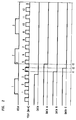
- the YCLK clock pulses are four times faster than the XCLK clock pulses, although the scope of the invention is not, of course, limited in this respect.
- DATA A is the received data pulse sampled by the XCLK clock pulse.
- the received data pulse sampled by the rising edge of the YCLK clock pulse is designated DATA B and the received data pulse sampled by the falling edge of the YCLK clock pulse is designated DATA C.
- sampling of the data pulse by the rising edge of the YCLK clock pulse produces the least phase quantization error with respect to the received data pulse, DATA, among the three alternatives illustrated.
- phase quantization error produced by timing recovery circuit 100 in this particular example may be reduced by retiming the received data signal to be synchronous with the rising edge of a YCLK clock pulse. Likewise, the phase quantization error may be even further reduced by increasing the YCLK clock frequency, if desired.
- FIG. 11 illustrates a similar approach with respect to the rising edge of a received data pulse.
- FIG. 2 illustrates that the received data pulse and oversampling clock YCLK may be employed to obtain a pulse edge proximity signal to reduce the phase quantization error associated with the recovered data signal produced by timing recovery circuit 100.
- circuitry to produce this proximity signal is provided, although the invention is not limited in scope to this particular embodiment.
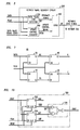
- FIG. 3 illustrates in more detail the embodiment of a refined timing recovery circuit 200 in accordance with the invention shown in FIG. 1.
- timing recovery circuit 200 includes a data pulse edge detector 250.
- data pulse edge detector refers to a circuit for sensing the next clock pulse edge of a digital clock pulse provided by an oversampling clock having closest temporal proximity after a selected received data pulse edge. Likewise, it may include a circuit for specifically sensing the next rising clock pulse edge or the next falling clock pulse edge.
- data pulse edge detector 250 is adapted to be coupled to an oversampling clock, YCLK, providing clock pulses at a substantially predetermined oversampling frequency.
- refined timing recovery circuit 200 also includes update control circuitry 350.
- update control circuitry 350 is employed to signal an update of the retiming applied to recovered data signals. If update control circuitry 350 signals an update, the recovered data signal is retimed substantially in accordance with the data pulse edge proximity signal being provided by data pulse edge detector 250.
- timing recovery circuit 100 provides a data valid signal to refined timing recovery circuit 200.
- FIG. 1 illustrates a timing delay between obtaining the received data pulse and obtaining the recovered data signal.
- the data valid signal is employed by update control circuitry 350 to signal an update of the retiming of the recovered data signal.
- FIG. 1 also illustrates that COUT may be provided to refined timing recovery circuit 200, although this detail is omitted from FIG. 3.
- recovered clock signal COUT may be employed by update control circuitry 250 to address a propagation delay problem that may arise where different delays affect the signals provided to retimer 300. This problem is avoided by timing any update based on the COUT signal, although this approach is not necessary for a refined timing recovery circuit or a timing recovery system in accordance with the present invention. By this approach, an update will not occur until the signals for retiming the recovered data signal are available to retimer 300 and relatively stable based on the timing provided by recovered clock signal, COUT.
- update control circuitry 350 may have on retiming the recovered data signal is illustrated at a high level in FIG. 3.
- data pulse edge detector 250 produces a proximity signal, designated "OR,” providing signal information regarding the temporal proximity of a falling data pulse edge to the rising or falling clock pulse edge of a clock pulse of the YCLK clock signal.
- proximity signal OR should not be confused with the boolean OR function, such as may be performed by a conventional digital logic gate.
- Proximity signal OR indicates whether the next occurring clock pulse edge after the data pulse falling edge is a rising or falling edge. This next clock pulse edge is produced by an oversampling clock.
- update control circuitry 350 provides an update control signal RFEN.
- proximity signal OR is combined with update control signal RFEN to produce the retiming edge signal, designated RF in FIG. 3.
- RFEN when RFEN is low, the last value of RF provided to retimer 300 is maintained. Thus, no update of the retiming of the recovered data signal occurs.
- RFEN when RFEN is high, retiming edge signal RF is updated to the value of proximity signal OR provided by data pulse edge detector 250.
- retimer 300 uses the RF signal to select the edge of the YCLK clock pulses, also provided to retimer 300 as illustrated in FIG. 3, to employ to retime the recovered data signal obtained from timing recovery circuit 100.
- retimer or “clock and data retimer” refers to a circuit for retiming the recovered data signal.
- retimer 300 retimes the recovered data signal to be synchronous with a selected edge of a YCLK clock pulse signaled by edge retiming signal RF.
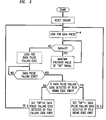
- FIG. 5 is a flow diagram illustrating the operation of a portion of an embodiment of a data pulse edge detector for use in a refined timing recovery circuit in accordance with the invention.
- FIG. 6 is a state diagram illustrating the operation of a portion of an embodiment of a data pulse edge detector for use in a refined timing recovery circuit in accordance with the invention
- FIG. 7 is a circuit diagram illustrating a portion of an embodiment of a data pulse edge detector for use in a refined timing recovery circuit in accordance with the invention.
- the flow diagram and the state diagram relate to a data pulse falling edge detector, in an alternative approach a data pulse rising edge detector may be employed.
- the circuit embodiment illustrated in FIG. 7 may be employed as a portion of either a data pulse rising edge detector or a data pulse falling edge detector, as explained in more detail hereinafter.
- a circuit embodiment such as the one illustrated in FIG. 7, may first be reset. Likewise, the circuit embodiment waits to receive a data pulse. If the data pulse received is a low signal, indicated in the flow chart by a zero, then the current recovered data signal is retimed substantially in accordance with the retiming applied to the last recovered data signal. This is indicated in the flow chart where the previous value of the proximity signal, OR, is maintained, as explained in more detail hereinafter. Alternatively, if the data pulse received is not low, the circuitry will have sensed the data pulse rising edge, at least for this particular embodiment. Therefore, the circuitry then waits for the data pulse falling edge.
- the circuitry determines whether the falling edge of the data pulse was detected by the rising edge or the falling edge of the YCLK clock pulse first. If the data pulse falling edge was detected by the rising edge of a YCLK clock pulse first, then the proximity signal is set high. Likewise, if the data pulse falling edge was detected by the falling edge of a YCLK clock pulse first, then the proximity signal is set low.
- a received data pulse, designated DATA, and YCLK clock pulses from an oversampling clock, such as an externally-derived oversampling clock are provided to this "front end" portion of data pulse edge detector 250.
- FIG. 4 is a timing diagram illustrating four types of input data pulses or data pulse signal patterns, designated A, B, C, and D, and the associated signals produced by the circuit embodiment illustrated in FIG. 7, the produced signals being designated RS, FS, R and F.
- signaling patterns A and B are referred to as fall-before-rise (FBR) patterns, in this context referring to the circumstance that the falling edge of both of these two signal patterns would be "captured” or latched by the falling edge of a YCLK clock pulse before the rising edge of a YCLK clock pulse. Therefore, the falling edge of a YCLK clock pulse is the next clock pulse edge in closest temporal proximity to the falling edge of the data pulse.
- FBR fall-before-rise
- signal patterns C and D are termed rise-before-fall (RBF) patterns, referring to the circumstance that the falling edge of these signaling patterns are "captured” or latched by the rising edge of a YCLK clock pulse before the falling edge of a YCLK clock pulse. Therefore, the rising edge of a YCLK clock pulse is the next clock pulse edge in closest temporal proximity to the falling edge of the data pulse.
- RBF rise-before-fall
- FIG. 4 illustrates in more detail the four signaling patterns and the corresponding sequences of signals provided by the portion of a circuit embodiment of a data pulse edge detector illustrated in FIG. 7 that may be incorporated in a refined timing recovery circuit in accordance with the invention.
- the embodiment illustrated in FIG. 7 includes circuitry providing signals indicating the next clock pulse edge in closest temporal proximity to the falling edge of the data pulse. As illustrated in FIG. 3, a proximity signal obtained based on the signals provided by this circuitry may then be combined with the RFEN signal obtained from the update control circuitry to provide an edge retiming signal (RF) to retimer 300.
- RF edge retiming signal
- the sequence of signals provided by the circuitry of the embodiment illustrated in FIG. 7 indicates the next clock pulse edge in closest temporal proximity to the falling edge of the data pulse signal. This is accomplished by the flip-flop configuration illustrated.
- the received data pulse is provided to the data (D) port of flip-flops 10 and 30.
- a YCLK clock signal is provided to the clock (CK) port of flip-flop 30, whereas an inverted YCLK clock signal is provided to the clock (CK) port of flip-flop 10.
- flip-flops 10 and 30 together are operating at effectively twice the frequency of the YCLK clock pulses, that is, one of flip-flops 10 and 30 latches the data pulse on alternative edges of a YCLK clock pulse, although individually each flip-flop is operating at the frequency of the YCLK clock pulses. Therefore, the signals provided at the output (Q) ports of flip-flops 10 and 30 produce signals providing signal information regarding the next clock pulse edge having the closest temporal proximity to the falling edge of the received data pulse. However, as suggested, these signals are being provided at twice the frequency of YCLK. Therefore, the signals designated in FIG.
- RS and FS may be provided to the remaining circuitry of the timing recovery system, although that circuitry would then operate at twice the frequency of YCLK as well.
- An enhancement of this approach is to employ flip-flops 20 and 40, as illustrated. Flip-flops 20 and 40 effectively reduce the frequency of the proximity signals provided by flip-flops 10 and 30 by a factor of two to thereby provide the proximity signal on the rising edge of a YCLK clock pulse, as illustrated in FIG. 4.
- the invention is not limited in scope to this particular embodiment.
- the signal transition sequence, RS, FS, R, and F, associated with each signaling pattern identified, i.e., A, B, C, and D, is provided in FIG. 4.
- the state diagram of FIG. 6 therefore illustrates how the signals provided by the circuit embodiment of FIG. 7 may be employed to sense the next clock pulse edge having the closest temporal proximity after the selected data pulse edge, in this case the falling data pulse edge.
- the circuit embodiment illustrated in FIG. 7 may also be employed to realize a data pulse rising edge detector.
- a state diagram other than the state diagram illustrated in FIG. 6 should be employed.
- signaling patterns A and C may constitute FBR patterns
- signaling patterns B and D may constitute RBF patterns.
- state diagram 255 includes four states designated 251, 252, 253, and 254.
- An embodiment of a data pulse edge detector to be incorporated in a refined timing recovery circuit in accordance with the invention may operate to sense either an RBF condition or an FBR condition, as previously described in connection with the description of FIG. 4.
- a high OR proximity signal is provided by the edge detector, such as to logic circuitry 450 as illustrated in FIG. 3.
- a low proximity OR signal may be provided.
- the scope of the invention is not limited to a particular signaling convention, such as the convention adopted in this particular embodiment.
- these signals provide signal information regarding the next clock pulse edge of a YCLK clock pulse in closest temporal proximity to the falling edge of the received data pulse.
- the input signals in accordance with the state diagram in FIG. 6 are the R and F signals provided by the circuit embodiment illustrated in FIG. 7. Also a RESET signal may be provided.
- the output signal, as previously described, is the proximity signal, OR.
- the convention "R,F/OR” is therefore employed along each state transition arc to designate the input/output signal values on a state transition.
- State 254 This is the initial state for this embodiment.
- proximity signal OR is high to signal a RBF start up condition.
- the edge detector transitions to State 253.
- this state addresses situations when RESET is active or the data pulse is low. The edge detector remains in this state in these situations.
- State 253 This state indicates that a data pulse has been obtained or received. As long as the data pulse remains high, the edge detector remains in this state. When the data pulse falling edge is detected, the edge detector transitions to either State 254 or State 252 according to whether an RBF or FBR condition is sensed.
- State 252 This state is similar to State 254 except that this state corresponds to an RBF condition.
- the edge detector remains in this state as long as data pulse is low and transitions to State 251 when the rising edge of a data pulse is sensed.
- State 251 This state indicates that the rising edge of a data pulse has been sensed. As long as the data pulse remains high, the edge detector remains in this state. When a data pulse falling edge is detected, the edge detector transitions to State 254 or State 252 depending on whether an RBF or FBR condition is sensed.
- FIG. 8 is a flow diagram illustrating the operation of an embodiment of update control circuitry, such as may be employed in a refined timing recovery circuit in accordance with the invention
- FIG. 9 is its state diagram. It will be appreciated that the invention is not restricted in scope to update control circuitry in accordance with these diagrams and, furthermore, a refined timing recovery circuit in accordance with the invention may not necessarily even employ update control circuitry, depending on the embodiment.
- update control circuitry is "reset," that is, update control signal RFEN remains low. The effect of this to to maintain the current value of edge retiming signal RF. This is desirable in this situation because the timing recovery system has not obtained additional timing signal information where the data pulse remains low.
- the circuitry waits for a valid data signal to be provided, such as by timing recovery circuitry 100, as previously described. If a data valid signal is received, the update control circuitry provides update control signal RFEN, set high in this embodiment. Then, as illustrated in FIG. 3, logic circuitry 450 updates edge retiming signal RF to the value of proximity signal OR based on update control signal RFEN. The updated edge retiming signal RF is provided to retimer 300, as illustrated in FIG. 1. As previously suggested, the invention is not restricted in scope to the particular signaling conventions employed in this particular embodiment.
- FIG. 9 is a state diagram for an embodiment of an update control circuit that may be employed in a refined timing recovery circuit in accordance with the invention.
- the input signals to the update control circuitry include a received data pulse, DATA, a data valid signal, DAV, obtained from timing recovery circuit 100, and a reset signal, RESET.
- update control signal RFEN is the output signal provided.
- the convention "DATA, DAV/RFEN" is employed along each state transition arc to designate the input/output signal values on a state transition.
- State 351 this is the initial or default state. In this state, the update control circuitry waits for the received data pulse or for the data valid signal for the data pulse just received. Likewise, where RESET is active or the data pulse is low, the circuitry remains in this state. The initial default value of RFEN is low. When the rising edge of a data pulse is sensed, the update control circuitry transitions to state 352. In State 351, if the data valid signal is high and is received coincidentally with the falling edge of the data pulse or the rising edge of the next data pulse, the update control circuitry provides update control signal RFEN as high to logic circuitry 450 in order to update edge retiming signal RF and transitions to State 355.
- State 352 This state indicates that the data pulse has begun. A rising edge of the data pulse has been sensed. The update control circuitry in this state waits for a valid data pulse. As long as a data pulse rising edge has been sensed and the data valid signal is low, the update control circuitry remains in this state. If the falling edge of the data pulse is sensed before a data valid signal occurs, a signaling "glitch" may have occurred. Therefore, the update control circuitry transitions to State 354 for further processing. With the data pulse high, if a data valid signal is received, the update control circuitry transitions to State 353 indicating that a valid data pulse has been received and waits for the data pulse to end. If the data pulse falling edge occurs coincidentally with the data valid signal, a transition to State 355 occurs and update control signal RFEN is set high to signal an update of edge retiming signal RF to the value of proximity signal OR.
- State 353 This state signals that a valid data signal has been received. As long as the data pulse is high, the update control circuitry remains in this state. When the falling edge of the data pulse is sensed, a transition to State 355 occurs and update control signal RFEN is set high to signal an update of edge retiming signal RF to the value of proximity signal OR.
- State 354 This state provides glitch rejection/tolerance for the update control circuitry. As described above with respect to State 352, a signaling glitch may cause the update control circuitry to transition from State 352 to this state.
- the update control circuitry transitions to State 351 confirming that a signaling glitch has occurred. In this context, this is referred to as a "glitch rejection.”
- a data pulse is high and the data valid signal is low, this indicates that data pulse signaling has resumed after only a short glitch. Under these circumstances, the update control circuitry returns to State 352.
- update control signal RFEN is set high to signal an update of edge retiming signal RF and a transition to State 355 occurs.
- State 355 This state signifies the end of a valid data pulse. When in this state, a low data pulse causes the update control circuitry to transition to State 351 and a data pulse that is high results in a transition to State 352.
- logic circuitry 450 may comprise, for example, a conventional flip-flop in which proximity signal OR is provided to the data (D) port of the flip-flop and update control signal RFEN is provided to the "ENABLE" port of the flip-flop.
- proximity signal OR is provided to the data (D) port of the flip-flop
- update control signal RFEN is provided to the "ENABLE" port of the flip-flop.
- the output (Q) port of the flip-flop produces edge retiming signal RF.
- RFEN is low, then the edge retiming signal RF is not updated to the value of proximity signal OR.
- FIG. 10 is a circuit diagram of a portion of an embodiment of retimer 300.
- edge retiming signal RF and YCLK clock pulses are provided to retimer 300.
- the recovered data signal previously described is provided to retimer 300.
- retimer 300 may retime the recovered data signal to be aligned with an edge of a YCLK clock pulse.
- the portion of retimer 300 illustrated in FIG. 10 illustrates retiming for the recovered clock signal COUT.
- a similar approach may also be applied for signals PDATA and NDATA.
- flip-flops 322 and 324 retime signal COUT to be synchronous with the rising edge of the YCLK clock pulse and the falling edge of the YCLK clock pulse, respectively.
- these alternatively retimed COUT signals are in effect multiplexed by block 326 based on edge retiming signal RF.
- a refined timing recovery circuit in accordance with the invention may be employed to sense the next clock pulse edge having closest temporal proximity to a selected received data pulse edge, such as either the data pulse rising edge or the data pulse falling edge. Nonetheless, the invention is not limited in scope to employing both edges of a clock pulse in this manner.
- a refined timing recovery circuit in accordance with the invention may alternatively sense the next rising clock pulse edge or the next falling clock pulse edge having closest temporal proximity to a selected received data pulse edge.
- Such an embodiment in accordance with the invention may still retain advantages in comparison with increasing the frequency of the XCLK clock pulse frequency, although the resolution will be reduced in comparison with an approach which employs both edges of a clock pulse, such as illustrated in FIG. 3, for example.
- the phase quantization error of a recovered data signal may be reduced in accordance with the following method.
- the recovered data signal is derived from a received data pulse by sampling with digital clock pulses at a first substantially predetermined frequency, denoted XCLK clock pulses in this context.
- the received data pulse may also be sampled with digital clock pulses at a second substantially predetermined frequency, denoted YCLK clock pulses in this context, so as to sense the next clock pulse edge of a digital clock pulse at the second substantially predetermined frequency in closest temporal proximity to a selected edge of the received data pulse.
- the selected edge may comprise either the rising edge of the data pulse or the falling edge of the data pulse.
- the second substantially predetermined frequency may be approximately M times the first substantially predetermined frequency, M being a positive integer, although the invention is not restricted in scope in this respect. As previously described, this may be accomplished by a data pulse edge detector that may be incorporated in a refined timing recovery circuit in accordance with the invention. For example, in the embodiment illustrated in FIG. 3, proximity signal OR signal indicates the next clock pulse edge in closest temporal proximity to a selected edge of the received data pulse.
- the recovered data signal may be retimed to be substantially aligned or synchronous with a clock pulse edge of a digital clock pulse at the second substantially predetermined frequency.
- the clock pulse edge employed to align or retime the received data signal corresponds to the next clock pulse edge sensed to be in closest temporal proximity to the selected edge of the received data pulse.
- the recovered data signal is retimed substantially in accordance with the clock pulse edge sensed as the next clock pulse edge in closest temporal proximity. This may be accomplished a variety of ways, such as the technique employed by the embodiment previously described.
- retimer 300 obtains an edge retiming signal RF which indicates whether to retime the recovered data signal on the rising edge of a YCLK clock pulse or the falling edge of a YCLK clock pulse.
- edge retiming signal RF indicates whether to retime the recovered data signal on the rising edge of a YCLK clock pulse or the falling edge of a YCLK clock pulse.
- refined timing recovery circuit 200 also includes update control circuitry 350.
- the effect of update control circuitry 350 is to delay the retiming step until after the data pulse is validated, in this particular embodiment by timing recovery circuit 100.
- the recovered data signal may be retimed regardless of whether it is validated or not, for example.
Landscapes
- Engineering & Computer Science (AREA)
- Computer Networks & Wireless Communication (AREA)
- Signal Processing (AREA)
- Synchronisation In Digital Transmission Systems (AREA)
- Stabilization Of Oscillater, Synchronisation, Frequency Synthesizers (AREA)
- Dc Digital Transmission (AREA)
Applications Claiming Priority (2)
| Application Number | Priority Date | Filing Date | Title |
|---|---|---|---|
| US315783 | 1994-09-30 | ||
| US08/315,783 US5539784A (en) | 1994-09-30 | 1994-09-30 | Refined timing recovery circuit |
Publications (2)
| Publication Number | Publication Date |
|---|---|
| EP0705003A2 true EP0705003A2 (de) | 1996-04-03 |
| EP0705003A3 EP0705003A3 (de) | 1997-07-23 |
Family
ID=23226037
Family Applications (1)
| Application Number | Title | Priority Date | Filing Date |
|---|---|---|---|
| EP95306620A Withdrawn EP0705003A3 (de) | 1994-09-30 | 1995-09-20 | Taktrückgewinnungsschaltung |
Country Status (6)
| Country | Link |
|---|---|
| US (2) | US5539784A (de) |
| EP (1) | EP0705003A3 (de) |
| JP (1) | JPH08125647A (de) |
| KR (1) | KR960012814A (de) |
| CN (1) | CN1126331A (de) |
| TW (1) | TW298693B (de) |
Cited By (3)
| Publication number | Priority date | Publication date | Assignee | Title |
|---|---|---|---|---|
| EP0839345A1 (de) * | 1996-04-19 | 1998-05-06 | Motorola, Inc. | Verfahren und system zur resynchronisation eines phasenverschobenen empfangenden datenstroms mit einem haupttakt |
| WO1998033292A1 (en) * | 1997-01-23 | 1998-07-30 | Ericsson Inc. | Digital phase aquisition with delay-locked loop |
| DE102005006172A1 (de) * | 2005-02-10 | 2006-08-24 | Siemens Ag | Schaltungsanordnung und Verfahren zur Datenübertragung |
Families Citing this family (29)
| Publication number | Priority date | Publication date | Assignee | Title |
|---|---|---|---|---|
| JP3347848B2 (ja) * | 1993-11-08 | 2002-11-20 | 株式会社ゼネラル リサーチ オブ エレクトロニックス | 多値信号復号回路 |
| JP3729366B2 (ja) * | 1996-11-29 | 2005-12-21 | 株式会社ゼネラル リサーチ オブ エレクトロニックス | パケットfsk受信機用クロック再生回路 |
| US6148038A (en) * | 1997-03-31 | 2000-11-14 | Sun Microsystems, Inc. | Circuit for detecting and decoding phase encoded digital serial data |
| US6249555B1 (en) | 1997-07-14 | 2001-06-19 | Grass Valley (Us) Inc. | Low jitter digital extraction of data from serial bitstreams |
| WO1999044327A2 (en) * | 1998-02-26 | 1999-09-02 | Koninklijke Philips Electronics N.V. | Clock recovery circuit and a receiver having a clock recovery circuit |
| US6377575B1 (en) | 1998-08-05 | 2002-04-23 | Vitesse Semiconductor Corporation | High speed cross point switch routing circuit with word-synchronous serial back plane |
| US6198700B1 (en) * | 1999-06-04 | 2001-03-06 | Level One Communications, Inc. | Method and apparatus for retiming test signals |
| US6292554B1 (en) * | 1999-10-07 | 2001-09-18 | Simplified Telesys | System and method for communicating with and controlling disparate telecommunications devices in a telecommunications network |
| US6775345B1 (en) | 1999-12-30 | 2004-08-10 | Intel Corporation | Delay locked loop based data recovery circuit for data communication |
| US6639956B1 (en) * | 1999-12-31 | 2003-10-28 | Intel Corporation | Data resynchronization circuit |
| EP1307820B1 (de) * | 2000-06-06 | 2014-07-23 | Vitesse Semiconductor Corporation | Koppelpunktvermittlung mit koppelmatrixmodul |
| US8155256B2 (en) * | 2000-10-23 | 2012-04-10 | Texas Instruments Incorporated | Method and apparatus for asynchronous clock retiming |
| GB2397733B (en) * | 2000-12-06 | 2004-10-06 | Fujitsu Ltd | Clock recovery circuitry |
| US6768385B2 (en) * | 2001-05-11 | 2004-07-27 | Mstar Semiconductor, Inc. | Intelligent phase lock loop |
| US7103125B1 (en) * | 2001-05-16 | 2006-09-05 | Lexmark International, Inc. | Method and apparatus for effecting synchronous pulse generation for use in serial communications |
| US7139344B2 (en) * | 2001-05-16 | 2006-11-21 | Lexmark International, Inc. | Method and apparatus for effecting synchronous pulse generation for use in variable speed serial communications |
| DE60125360D1 (de) * | 2001-09-18 | 2007-02-01 | Sgs Thomson Microelectronics | Abfrageprüfgerät, das Überabtastung zur Synchronisierung verwendet |
| US6888905B1 (en) * | 2001-12-20 | 2005-05-03 | Microtune (San Diego), Inc. | Low deviation index demodulation scheme |
| DE10207315B4 (de) * | 2002-02-21 | 2007-01-04 | Infineon Technologies Ag | Vorrichtung zur Datenrückgewinnung aus einem empfangenen Datensignal |
| US7349498B2 (en) * | 2002-10-07 | 2008-03-25 | International Business Machines Corporation | Method and system for data and edge detection with correlation tables |
| CN100352194C (zh) * | 2003-04-23 | 2007-11-28 | 华为技术有限公司 | 调节采样时钟保障同步数据可靠接收的方法及其装置 |
| EP1992955B1 (de) * | 2003-12-17 | 2012-07-25 | STMicroelectronics (Research & Development) Limited | TAP-Multiplexer |
| CN100481236C (zh) * | 2005-01-26 | 2009-04-22 | 宏阳科技股份有限公司 | 全数字式频率/相位恢复电路 |
| JP4213132B2 (ja) * | 2005-03-28 | 2009-01-21 | 富士通マイクロエレクトロニクス株式会社 | タイミングリカバリ回路及び間引きクロック生成方法 |
| KR100819097B1 (ko) * | 2006-12-05 | 2008-04-02 | 삼성전자주식회사 | 랜덤 에지 샘플링을 이용한 클럭 및 데이터 복원회로 및그 복원방법 |
| JP4942195B2 (ja) * | 2007-02-27 | 2012-05-30 | キヤノン株式会社 | データ通信装置、データ通信システム及びデータ通信方法 |
| CN101610083B (zh) * | 2009-06-19 | 2012-10-10 | 中兴通讯股份有限公司 | 一种高速多路时钟数据恢复电路 |
| CN102347813B (zh) | 2011-09-26 | 2015-11-25 | 华为技术有限公司 | 一种选取采样时钟信号的方法和设备 |
| US9520989B2 (en) * | 2014-07-28 | 2016-12-13 | Texas Instruments Incorporated | Phase detector and retimer for clock and data recovery circuits |
Family Cites Families (10)
| Publication number | Priority date | Publication date | Assignee | Title |
|---|---|---|---|---|
| FR2536610A1 (fr) * | 1982-11-23 | 1984-05-25 | Cit Alcatel | Equipement de transmission synchrone de donnees |
| US4663769A (en) * | 1985-10-02 | 1987-05-05 | Motorola, Inc. | Clock acquisition indicator circuit for NRZ data |
| US4821297A (en) * | 1987-11-19 | 1989-04-11 | American Telephone And Telegraph Company, At&T Bell Laboratories | Digital phase locked loop clock recovery scheme |
| US4972443A (en) * | 1987-11-24 | 1990-11-20 | Siemens Aktiengesellschaft | Method and arrangement for generating a correction signal for a digital clock recovery means |
| US4847870A (en) * | 1987-11-25 | 1989-07-11 | Siemens Transmission Systems, Inc. | High resolution digital phase-lock loop circuit |
| US4821295A (en) * | 1987-11-30 | 1989-04-11 | Tandem Computers Incorporated | Two-stage synchronizer |
| US4862482A (en) * | 1988-06-16 | 1989-08-29 | National Semiconductor Corporation | Receiver for Manchester encoded data |
| US4912730A (en) * | 1988-10-03 | 1990-03-27 | Harris Corporation | High speed reception of encoded data utilizing dual phase resynchronizing clock recovery |
| US5164966A (en) * | 1991-03-07 | 1992-11-17 | The Grass Valley Group, Inc. | Nrz clock and data recovery system employing phase lock loop |
| US5491713A (en) * | 1993-04-28 | 1996-02-13 | Hughes Aircraft Company | Minimized oversampling Manchester decoder |
-
1994
- 1994-09-30 US US08/315,783 patent/US5539784A/en not_active Expired - Lifetime
- 1994-10-12 TW TW083109443A patent/TW298693B/zh not_active IP Right Cessation
-
1995
- 1995-09-20 EP EP95306620A patent/EP0705003A3/de not_active Withdrawn
- 1995-09-27 KR KR1019950032007A patent/KR960012814A/ko not_active Application Discontinuation
- 1995-09-27 JP JP7272101A patent/JPH08125647A/ja active Pending
- 1995-09-29 CN CN95117369A patent/CN1126331A/zh active Pending
-
1996
- 1996-01-11 US US08/584,497 patent/US5689533A/en not_active Expired - Lifetime
Non-Patent Citations (1)
| Title |
|---|
| None |
Cited By (5)
| Publication number | Priority date | Publication date | Assignee | Title |
|---|---|---|---|---|
| EP0839345A1 (de) * | 1996-04-19 | 1998-05-06 | Motorola, Inc. | Verfahren und system zur resynchronisation eines phasenverschobenen empfangenden datenstroms mit einem haupttakt |
| EP0839345A4 (de) * | 1996-04-19 | 2002-05-29 | Motorola Inc | Verfahren und system zur resynchronisation eines phasenverschobenen empfangenden datenstroms mit einem haupttakt |
| WO1998033292A1 (en) * | 1997-01-23 | 1998-07-30 | Ericsson Inc. | Digital phase aquisition with delay-locked loop |
| US6044122A (en) * | 1997-01-23 | 2000-03-28 | Ericsson, Inc. | Digital phase acquisition with delay locked loop |
| DE102005006172A1 (de) * | 2005-02-10 | 2006-08-24 | Siemens Ag | Schaltungsanordnung und Verfahren zur Datenübertragung |
Also Published As
| Publication number | Publication date |
|---|---|
| EP0705003A3 (de) | 1997-07-23 |
| US5689533A (en) | 1997-11-18 |
| KR960012814A (ko) | 1996-04-20 |
| TW298693B (de) | 1997-02-21 |
| CN1126331A (zh) | 1996-07-10 |
| JPH08125647A (ja) | 1996-05-17 |
| US5539784A (en) | 1996-07-23 |
Similar Documents
| Publication | Publication Date | Title |
|---|---|---|
| US5539784A (en) | Refined timing recovery circuit | |
| EP0709966B1 (de) | Phasendetektor mit ternärem Ausgang | |
| US6614314B2 (en) | Non-linear phase detector | |
| US6002279A (en) | Clock recovery circuit | |
| US8442178B2 (en) | Linear phase detector and clock/data recovery circuit thereof | |
| US7215207B2 (en) | Phase and frequency detection circuits for data communication systems | |
| US6838945B2 (en) | Data resynchronization circuit | |
| US7684531B2 (en) | Data recovery method and data recovery circuit | |
| US5301196A (en) | Half-speed clock recovery and demultiplexer circuit | |
| US5633899A (en) | Phase locked loop for high speed data capture of a serial data stream | |
| US7170964B2 (en) | Transition insensitive timing recovery method and apparatus | |
| US6374361B1 (en) | Skew-insensitive low voltage differential receiver | |
| US7138837B2 (en) | Digital phase locked loop circuitry and methods | |
| US6236697B1 (en) | Clock recovery for multiple frequency input data | |
| US5864250A (en) | Non-servo clock and data recovery circuit and method | |
| US6850580B1 (en) | Bit synchronizing circuit | |
| US7183864B1 (en) | Ring oscillator for use in parallel sampling of high speed data | |
| US6389090B2 (en) | Digital clock/data signal recovery method and apparatus | |
| EP0463380A1 (de) | Schaltung zur Regeneration und zur seriellen Parallelumwandlung digitaler Daten | |
| US6421404B1 (en) | Phase-difference detector and clock-recovery circuit using the same | |
| US6868134B2 (en) | Method and apparatus for recovering a clock signal from an asynchronous data signal | |
| US7826581B1 (en) | Linearized digital phase-locked loop method for maintaining end of packet time linearity | |
| US7231009B2 (en) | Data synchronization across an asynchronous boundary using, for example, multi-phase clocks | |
| US7023944B2 (en) | Method and circuit for glitch-free changing of clocks having different phases | |
| US5930311A (en) | Circuitry for retiming a received data signal |
Legal Events
| Date | Code | Title | Description |
|---|---|---|---|
| PUAI | Public reference made under article 153(3) epc to a published international application that has entered the european phase |
Free format text: ORIGINAL CODE: 0009012 |
|
| AK | Designated contracting states |
Kind code of ref document: A2 Designated state(s): DE ES FR GB IT |
|
| PUAL | Search report despatched |
Free format text: ORIGINAL CODE: 0009013 |
|
| AK | Designated contracting states |
Kind code of ref document: A3 Designated state(s): DE ES FR GB IT |
|
| 17P | Request for examination filed |
Effective date: 19980108 |
|
| STAA | Information on the status of an ep patent application or granted ep patent |
Free format text: STATUS: THE APPLICATION HAS BEEN WITHDRAWN |
|
| 18W | Application withdrawn |
Withdrawal date: 19990109 |