EP0703679A2 - Circuit de surveillance simultanée de plusieurs longueurs d'ondes utilisant un réseau de guides d'ondes groupés - Google Patents
Circuit de surveillance simultanée de plusieurs longueurs d'ondes utilisant un réseau de guides d'ondes groupés Download PDFInfo
- Publication number
- EP0703679A2 EP0703679A2 EP95306741A EP95306741A EP0703679A2 EP 0703679 A2 EP0703679 A2 EP 0703679A2 EP 95306741 A EP95306741 A EP 95306741A EP 95306741 A EP95306741 A EP 95306741A EP 0703679 A2 EP0703679 A2 EP 0703679A2
- Authority
- EP
- European Patent Office
- Prior art keywords
- wavelength
- signal
- monitoring circuit
- simultaneous monitoring
- means comprises
- Prior art date
- Legal status (The legal status is an assumption and is not a legal conclusion. Google has not performed a legal analysis and makes no representation as to the accuracy of the status listed.)
- Granted
Links
Images


Classifications
-
- H—ELECTRICITY
- H04—ELECTRIC COMMUNICATION TECHNIQUE
- H04B—TRANSMISSION
- H04B10/00—Transmission systems employing electromagnetic waves other than radio-waves, e.g. infrared, visible or ultraviolet light, or employing corpuscular radiation, e.g. quantum communication
- H04B10/50—Transmitters
- H04B10/501—Structural aspects
- H04B10/506—Multiwavelength transmitters
-
- G—PHYSICS
- G02—OPTICS
- G02B—OPTICAL ELEMENTS, SYSTEMS OR APPARATUS
- G02B6/00—Light guides; Structural details of arrangements comprising light guides and other optical elements, e.g. couplings
- G02B6/10—Light guides; Structural details of arrangements comprising light guides and other optical elements, e.g. couplings of the optical waveguide type
- G02B6/12—Light guides; Structural details of arrangements comprising light guides and other optical elements, e.g. couplings of the optical waveguide type of the integrated circuit kind
- G02B6/12007—Light guides; Structural details of arrangements comprising light guides and other optical elements, e.g. couplings of the optical waveguide type of the integrated circuit kind forming wavelength selective elements, e.g. multiplexer, demultiplexer
- G02B6/12009—Light guides; Structural details of arrangements comprising light guides and other optical elements, e.g. couplings of the optical waveguide type of the integrated circuit kind forming wavelength selective elements, e.g. multiplexer, demultiplexer comprising arrayed waveguide grating [AWG] devices, i.e. with a phased array of waveguides
- G02B6/12011—Light guides; Structural details of arrangements comprising light guides and other optical elements, e.g. couplings of the optical waveguide type of the integrated circuit kind forming wavelength selective elements, e.g. multiplexer, demultiplexer comprising arrayed waveguide grating [AWG] devices, i.e. with a phased array of waveguides characterised by the arrayed waveguides, e.g. comprising a filled groove in the array section
-
- G—PHYSICS
- G02—OPTICS
- G02B—OPTICAL ELEMENTS, SYSTEMS OR APPARATUS
- G02B6/00—Light guides; Structural details of arrangements comprising light guides and other optical elements, e.g. couplings
- G02B6/10—Light guides; Structural details of arrangements comprising light guides and other optical elements, e.g. couplings of the optical waveguide type
- G02B6/12—Light guides; Structural details of arrangements comprising light guides and other optical elements, e.g. couplings of the optical waveguide type of the integrated circuit kind
- G02B6/12007—Light guides; Structural details of arrangements comprising light guides and other optical elements, e.g. couplings of the optical waveguide type of the integrated circuit kind forming wavelength selective elements, e.g. multiplexer, demultiplexer
- G02B6/12009—Light guides; Structural details of arrangements comprising light guides and other optical elements, e.g. couplings of the optical waveguide type of the integrated circuit kind forming wavelength selective elements, e.g. multiplexer, demultiplexer comprising arrayed waveguide grating [AWG] devices, i.e. with a phased array of waveguides
- G02B6/12019—Light guides; Structural details of arrangements comprising light guides and other optical elements, e.g. couplings of the optical waveguide type of the integrated circuit kind forming wavelength selective elements, e.g. multiplexer, demultiplexer comprising arrayed waveguide grating [AWG] devices, i.e. with a phased array of waveguides characterised by the optical interconnection to or from the AWG devices, e.g. integration or coupling with lasers or photodiodes
-
- G—PHYSICS
- G02—OPTICS
- G02B—OPTICAL ELEMENTS, SYSTEMS OR APPARATUS
- G02B6/00—Light guides; Structural details of arrangements comprising light guides and other optical elements, e.g. couplings
- G02B6/10—Light guides; Structural details of arrangements comprising light guides and other optical elements, e.g. couplings of the optical waveguide type
- G02B6/12—Light guides; Structural details of arrangements comprising light guides and other optical elements, e.g. couplings of the optical waveguide type of the integrated circuit kind
- G02B6/12007—Light guides; Structural details of arrangements comprising light guides and other optical elements, e.g. couplings of the optical waveguide type of the integrated circuit kind forming wavelength selective elements, e.g. multiplexer, demultiplexer
- G02B6/12009—Light guides; Structural details of arrangements comprising light guides and other optical elements, e.g. couplings of the optical waveguide type of the integrated circuit kind forming wavelength selective elements, e.g. multiplexer, demultiplexer comprising arrayed waveguide grating [AWG] devices, i.e. with a phased array of waveguides
- G02B6/12033—Light guides; Structural details of arrangements comprising light guides and other optical elements, e.g. couplings of the optical waveguide type of the integrated circuit kind forming wavelength selective elements, e.g. multiplexer, demultiplexer comprising arrayed waveguide grating [AWG] devices, i.e. with a phased array of waveguides characterised by means for configuring the device, e.g. moveable element for wavelength tuning
-
- H—ELECTRICITY
- H04—ELECTRIC COMMUNICATION TECHNIQUE
- H04B—TRANSMISSION
- H04B10/00—Transmission systems employing electromagnetic waves other than radio-waves, e.g. infrared, visible or ultraviolet light, or employing corpuscular radiation, e.g. quantum communication
- H04B10/50—Transmitters
- H04B10/572—Wavelength control
-
- G—PHYSICS
- G02—OPTICS
- G02B—OPTICAL ELEMENTS, SYSTEMS OR APPARATUS
- G02B6/00—Light guides; Structural details of arrangements comprising light guides and other optical elements, e.g. couplings
- G02B6/10—Light guides; Structural details of arrangements comprising light guides and other optical elements, e.g. couplings of the optical waveguide type
- G02B6/12—Light guides; Structural details of arrangements comprising light guides and other optical elements, e.g. couplings of the optical waveguide type of the integrated circuit kind
- G02B2006/12133—Functions
- G02B2006/12135—Temperature control
Definitions
- the present invention relates to a multiwavelength simultaneous monitoring circuit employing arrayed-waveguide grating preferably used as a wavelength meter in optical communication networks using wavelength division multiplexing (WDM) technologies, or as a wavelength discriminator in a stabilizing circuit for wavelength division multiplexing optical sources.
- WDM wavelength division multiplexing
- Optical sources used in WDM networks are chiefly laser diodes whose oscillation wavelengths vary with aging or changes in the ambient temperature. Accordingly, it is necessary to measure the wavelengths of a number of laser diodes simultaneously and accurately.
- a conventional multiwavelength monitoring circuit that monitors individual wavelengths of a WDM signal carries out wavelength discrimination by scanning the center transmission wavelength of a scanning optical filter (for example, a scanning Fabry-Perot interferometer) on time basis, and thus converting wavelength errors into time domain values, the wavelength errors corresponding to the differences between the wavelength of the WDM signals and the center wavelength of the optical filters.
- a scanning optical filter for example, a scanning Fabry-Perot interferometer
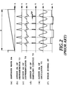
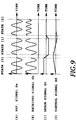
- Fig. 1 shows a configuration of a conventional multiwavelength monitoring circuit (T. Mizuochi, et al., "622 Mbit/s-Sixteen-Channel FDM Coherent Optical Transmission System Using Two-Section MQW DFB-LDs", The transactions of the Institute of Electronics, Information and Communication Engineers of Japan, B-I, Vol. J77-B-1, No. 5, pp. 294-303, 1994).
- a reference optical signal R and a WDM signal W are multiplexed through an optical coupler 71, and injected into a scanning Fabry-Perot interferometer 72.
- the scanning Fabry-Perot interferometer 72 carries out scanning using a sawtooth wave (Fig. 2(a)) generated by a sawtooth generator 76 synchronized with an oscillator 75, and an optical signal whose center wavelength coincides with a center transmission wavelength of the Fabry-Perot interferometer 72 is received by a photodetector 73.
- the output pulses (Fig. 2(b)) of the photodetector 73 are differentiated by a differentiator 78 to detect peak positions of the output pulses (Fig. 2(c)).
- the sampling pulses are generated by a sampling circuit 79 at the peak positions of the output optical pulses in Fig. 2(b).
- the sampling pulses and the output of the oscillator 75 (Fig. 2(e)) are inputted into a coherent detector 80 whose output is inputted into a sample-and-hold circuit 81. Since the sawtooth wave and the output signal of the oscillator 75 are synchronized, phases of the output signal of the oscillator 75 can be detected by the sampling pulses.
- the sample-and-hold circuit 81 holds the detected phases, thus producing an error signal as shown in Fig. 2(f).
- a selector 74 sequentially outputs relative error signals between the center transmission wavelength of the scanning Fabry-Perot interferometer 72 and the wavelengths of the reference optical signal R and the WDM signal W.
- the error signal associated with the reference optical signal R is added by an adder 77 to the sawtooth wave outputted from the sawtooth generator 76, and is applied to the scanning Fabry-Perot interferometer 72, so that the positions of the output pulses of the photodetector 73 associated with the reference optical signal R are controlled to be locked at a correct position.
- the center transmission wavelength of the scanning Fabry-Perot interferometer 72 can be stabilized using the wavelength of the reference optical signal R, thereby achieving temperature compensation function for variations in the ambient temperature.
- the error signals associated with individual wavelengths of the WDM signal W is negatively fed back to respective optical sources of the WDM signal W to control the injection currents or temperature of the optical sources, thereby locking the wavelengths of the WDM signal W.
- the conventional scanning Fabry-Perot interferometer can be implemented in a rather simple optical circuit, although a mechanism for scanning the cavity length with piezoelectric device is required. Furthermore, the scanning Fabry-Perot interferometer has an advantage in that wavelength variations can be monitored in a wide range at a desired resolution by appropriately setting its center transmission wavelength and bandwidth.
- the monitoring circuit comprising: an AWG (arrayed-waveguide grating) including at least one first channel outputting at least a part of the reference optical signal when the reference optical signal and the WDM signal are inputted, and at least one second channel outputting at least a part of the optical signal Sk for each of the optical signals Sk; a first photodetecting means for detecting the reference optical signal outputted from the first channel; a second photodetecting means for detecting the optical signal Sk outputted from the second channel; control means for stabilizing the center transmission wavelength of the first channel on the basis of an output from the first photodetecting means; and wavelength error detecting means for producing an error signal indicative of a
- the control means may comprise: modulating means for providing modulation so that the first channel outputs a modulated reference optical signal; a first coherent detector for coherently detecting the output of the first photodetecting means; and a first detector for detecting a wavelength error of a wavelength of the reference optical signal on the basis of an output of the first coherent detector, wherein the center transmission wavelength of the first channel is stabilized on the basis of an output of the first detector.
- the AWG may comprise two first channels associated with the reference optical signal, and two second channels associated with each optical signal Sk of the optical signals Sk, and wherein the monitoring circuit further comprises: a first comparing means for comparing powers of two optical outputs produced from the first channels; and a second comparing means for comparing powers of two optical outputs produced from the second channels; and wherein the control means stabilizes the center transmission wavelengths of the first channels on the basis of an output of the first comparing means, and the wavelength error detecting means detects wavelength error of the optical signal Sk on the basis of an output of the second comparing means.
- the control means may comprise an offset circuit generating an offset signal indicative of a difference between the wavelength of the reference optical signal and the center transmission wavelength of the first channel associated with the reference optical signal, and wherein the control means adds the offset signal to a difference between a wavelength of the reference optical signal and an actual center transmission wavelength of the first channel to obtain a summing result, and controls so that the center transmission wavelength of the first channel coincides with a predetermined center transmission wavelength on the basis of the summing result.
- the modulating means may simultaneously modulate respective channels of the AWG.
- the modulating means may modulate the WDM signal and the reference optical signal, and injects a modulated optical signal into at least one of the channels of the AWG.
- the wavelength error detecting means may comprise: a second coherent detector for coherently detecting an output signal of the second photodetecting means; and a second detector for detecting a wavelength error of the optical signal Sk of the WDM signal on the basis of an output of the second coherent detector.
- the multiwavelength simultaneous monitoring circuit may further comprise input means for injecting the WDM signal and the reference optical signal simultaneously into one of the channels of the AWG .
- the multiwavelength simultaneous monitoring circuit may further comprise input means for injecting the WDM signal and the reference optical signal separately into different channels of the AWG.
- the multiwavelength simultaneous monitoring circuit may further comprise input means for splitting a multiplexed signal of the WDM signal and the reference optical signal, and for injecting the split multiplexed signal into separate channels of the AWG.
- the two first channels may be adjacent to each other, and the two second channels may be adjacent to each other.
- the two first channels may be separated apart by an amount corresponding to an FSR (Free Spectral Range), and the two second channels are separated apart by the amount corresponding to the FSR.
- FSR Free Spectral Range
- the first comparing means may comprise a logarithmic amplifier, and the second comparing means comprises a logarithmic amplifier.
- the first comparing means may comprise an A/D converter and a digital signal processor
- the second comparing means comprises an A/D converter and a digital signal processor
- the first comparing means may comprise a differential photodetector, and the second comparing means comprises a differential photodetector.
- the center transmission wavelength or the crossover wavelength of the reference channel of the AWG (Arrayed-Waveguide Grating) is controlled so that the center transmission wavelength or the crossover wavelength of the reference channel is locked to the wavelength of the reference optical signal.
- the relative accuracy of the periodic center transmission wavelengths or the crossover wavelengths of the AWG is extremely high, the transmission characteristics of the entire port of the AWG can be stabilized by locking the center transmission wavelength or the crossover wavelength of the reference channel to the reference wavelength. Detecting the relative wavelength errors of individual wavelengths of the WDM signal in this state can achieve highly accurate, stable wavelength discrimination.
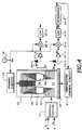
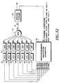
- Fig. 4 shows a configuration of a first embodiment of a multiwavelength simultaneous monitoring circuit in accordance with the present invention.
- a reference optical signal (wavelength ⁇ 0) and a WDM signal to be monitored (wavelength ⁇ 1 - ⁇ n ) are inputted to a predetermined input waveguide of an AWG (Arrayed-Waveguide Grating) 12 after multiplexed by an optical coupler 11.
- the AWG 12 includes the following elements which are connected in this order: an input waveguide array 32 formed on a substrate 31; an input concave-slab waveguide 33; a waveguide array 34 including a plurality of waveguides which progressively become longer by a length difference ⁇ L, an output concave-slab waveguide 35; and an output waveguide array 36.
- the waveguide array 34 is provided with a heater 13 connected to a current source 15.
- the current source 15 is supplied with a reference signal Sa outputted from an oscillator 14, and controls the temperature of the heater 13 in response to the reference signal Sa.
- the outputs of the photodetectors 16-0 and 16-i are connected to phase comparators 18-0 and 18-i through amplifiers 17-0 and 17-i, respectively.
- the phase comparators 18-0 and 18-i are provided with the reference signal Sa outputted from the oscillator 14, and their outputs are inputted to low-pass filters (LPFs) 19-0 and 19-i.
- the output of the low-pass filter 19-0 is supplied to an integrator 20-0.
- the output (wavelength error signal Sd) of the integrator 20-0 is fed to a temperature control circuit 21 that controls a Peltier cooler 22 for regulating the temperature of the AWG 12.
- Fig. 6 is a block diagram showing the configuration of a temperature control circuit 21.
- the reference numeral 121 designates a thermistor for detecting the temperature of the AWG 12.
- the output of the thermistor 121 is fed to a thermistor bridge circuit 211 in the temperature control circuit 21.
- the thermistor bridge circuit 211 outputs a temperature signal TS corresponding to the temperature of the AWG 12 on the basis of the resistance of the thermistor 121, and supplies it to a first input terminal of a comparator 212.
- a second input terminal of the comparator 212 is provided with a reference voltage RV from a reference voltage source 213.
- the comparator 212 compares the temperature signal TS and the reference voltage RV, and outputs an error signal TE between a measured temperature and a set temperature.
- the error signal is supplied to a loop filter 214 with a predetermined time constant.
- the loop filter 214 converts the error signal TE to a temperature control signal TC.
- the wavelength error signal Sd associated with the reference optical signal is supplied to an adder 215.
- the wavelength error signal Sd indicates a difference between the wavelength of the reference optical signal and the center transmission wavelength of the channel corresponding to the reference optical signal.
- the sum of the wavelength error signal Sd and an offset signal FS indicates the difference between the set center transmission wavelength and the actual center transmission wavelength.
- the adder 215 adds the wavelength error signal Sd to the offset signal FS supplied from an offset circuit 216, and provides a next adder 217 with an error signal ES.
- the adder 217 obtains the difference between the error signal ES and the temperature control signal TC, and controls the Peltier cooler 22 through a Peltier element driver 218.
- the offset signal indicative of the difference between the set center transmission wavelength of the AWG 12 and the reference wavelength it becomes possible to control the center transmission wavelengths of the AWG 12 by the reference optical signal with a wavelength different from the set center transmission wavelength.
- the photodetectors 16-i connected to the output waveguides #1 - #n of the AWG 12 may be replaced by a set of an optical switch 23 and the photodetector 16-1, the optical switch 23 selecting one of the outputs of the output waveguides #1 - #n and supplying it to the photodetector 16-1.
- An optical signal injected into a predetermined waveguide of the input waveguide array 32 spreads in the input concave-slab waveguide 33 by diffraction, and is guided to the waveguide array 34 disposed perpendicularly to the diffraction surface of the input concave-slab waveguide 33. Since the respective waveguides of the waveguide array 34 are progressively lengthened by an amount of waveguide length difference ⁇ L, optical signals passing through the waveguides and reaching the output concave-slab waveguides 35 have phase differences corresponding to the waveguide length differences ⁇ L. Since the phase differences vary in accordance with the wavelengths (optical frequencies), the output concave-slab waveguide 35 focuses through its lensing effect the optical signals on different input terminals of the output waveguide array 36 in accordance with the wavelengths.
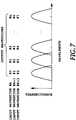
- the AWG 12 functions as an optical demultiplexer having transmission characteristics as shown in Fig. 7.
- the center transmission wavelengths are spaced at a fixed interval corresponding to the output waveguides.
- the correspondence between the center transmission wavelengths and the output waveguides periodically shifts by one channel when the input waveguide is shifted by one position.
- the temperature of the heater 13 for heating the waveguide array 34 is varied in response to the reference signal Sa.
- This provides the transmission characteristics of the AWG 12 with small vibrations on the wavelength axis as shown in Figs. 8, 10A and 10B.
- the small vibrations in turn provides the output optical signals with the variation in power.
- carrying out the coherent detection of the variations in power makes it possible to detect wavelength errors between the wavelengths of the input optical signals and the center transmission wavelengths.
- the center transmission wavelength of the reference channel is first matched to the reference wavelength, thereby stabilizing the transmission characteristics of the AWG 12.
- Figs. 8 and 9 illustrate the operation for discriminating the reference wavelength, and stabilizing the transmission characteristics in the first embodiment.
- the reference optical signal is launched from the output waveguide #0 of the AWG 12, and is received by the photodetector 16-0.
- the output of the photodetector 16-0 is amplified by the amplifier 17-0, and the amplified signal Sb is inputted to the phase comparator 18-0.
- the center transmission wavelength of the output waveguide #0 takes one of the three states [1], [2] and [3] with respect to the reference wavelength ⁇ 0 as shown in Figs. 8 and 9.
- the received signal Sb undergoes coherent detection in the phase comparator 18-0 using the reference signal Sa, followed by removal of the small vibration component through the lowpass filter 19-0 to extract a signal component, thereby obtaining an error signal Sc corresponding to the relative wavelength difference between the reference wavelength ⁇ 0 and the center transmission wavelength of the output waveguide #0.
- the error signal Sc will become positive in the state [3], negative in the state [1], and zero in the state [2].
- the error signal Sc is subject to time integration by the integrator 20-0 to obtain a control signal Sd which is fed back to the AWG 12 through the temperature control circuit 21 and the Peltier cooler 22.
- the transmission characteristics of the AWG 12 can also be varied by the temperature control with the Peltier cooler 22.
- the loop for regulating the relative wavelength difference to zero operates, so that the center transmission wavelength of the output waveguide #0 of the AWG 12 can be locked to the reference wavelength ⁇ 0.
- Stabilizing the center transmission wavelengths of the output waveguides #1 - #n of the AWG 12 at the wavelengths ⁇ 1, ⁇ 2, ..., ⁇ n of the WDM signal to be monitored makes it possible to detect errors of the individual wavelengths of the WDM signal by coherently detecting the output optical signals from the respective output waveguides.
- the intervals between adjacent wavelengths of the WDM signal can be equal or not equal.
- the AWG 12 can handle either cases.
- Figs. 10A and 10B illustrate the wavelength discrimination of the WDM signal in the first embodiment.
- error signals detected by the coherent detection in the phase comparators 18-1 - 18-n correspond to the relative wavelength differences between the respective wavelengths ⁇ 1 - ⁇ n of the WDM signal and the center transmission wavelengths of the output waveguides #1 - #n.
- the state [1] in Fig. 10B in which the wavelength ⁇ 1 shifts to the short wavelength side, is equivalent to the state [1] of Figs. 8 and 9, in which the center transmission wavelength of the output waveguide #0 shifts to the long wavelength side with respect to the reference wavelength ⁇ 0.
- the state [3], in which the optical signal of wavelength ⁇ 1 shifts to the long wavelength side is equivalent to the state [3] of Figs. 8 and 9, in which the center transmission wavelength of the output waveguide #0 shifts to the short wavelength side with respect to the reference wavelength ⁇ 0.
- an error signal proportional to fluctuations of the wavelength can be obtained by the coherent detection centered on the state [2] corresponding to the center transmission wavelength ⁇ 1 of the output waveguide #1.
- error signals corresponding to respective wavelength differences of the WDM signal can be digitized, or fed back to wavelength control circuits of individual optical sources of the WDM signal. This will be described in more detail with reference to Fig. 32.
- the multiwavelength simultaneous monitoring circuit of this embodiment can discriminate the wavelength errors of the WDM signal to be monitored at high accuracy by utilizing the highly accurate relationships between the center transmission wavelengths of the output waveguides of the AWG 12, and by locking one of the center transmission wavelengths to the reference wavelength ⁇ 0.
- the reference optical signal and the WDM signal are multiplexed before injected into a predetermined input waveguide of the AWG 12 in this embodiment, they may be injected into different input waveguides. This enables one of the wavelengths of the WDM signal to be utilized as the reference wavelength, as well. Since the output waveguides shift periodically with the shift of the input waveguide as will be described later, a reference optical signal with a wavelength equal to one of the wavelengths of the WDM signal can be made to emit from the output waveguide #0 by injecting it to an input waveguide different from that of the WDM signal. For example, in the wavelength allocation as shown in Fig.
- a reference optical signal with a wavelength ⁇ 1 or ⁇ n should be injected into an input waveguide adjacent to that of the WDM signal.
- the reference optical signal can take any desired wavelength including those of the WDM signal. This will be described in more detail later with reference to Figs. 29A and 29B.
- Fig. 11 is a block diagram showing a second embodiment of the multiwavelength simultaneous monitoring circuit in accordance with the present invention.
- an optical signal to be injected into the AWG 12 is frequency modulated by the reference signal Sa in this embodiment.
- a phase modulator or frequency modulator 24 is provided between the optical coupler 11 and the AWG 12 so as to phase modulate or frequency modulate the reference optical signal R and the WDM signal W by supplying the phase modulator or frequency modulator 24 with the reference signal Sa outputted from the oscillator 14.
- the remaining portion and the wavelength error detection principle are similar to those of the first embodiment.
- the transmission characteristic of the AWG 12 are kept constant, whereas the reference optical signal R and WDM signal W are provided with small oscillation on the wavelength axis, so that the variation in the power of the received signal Sb is detected by the coherent detection in response to the oscillation, thereby detecting the relative wavelength difference with respect to the center transmission wavelengths. Accordingly, the sign of the error signals of this embodiment has opposite sense as that of the first embodiment.
- Figs. 12 and 13 illustrate the wavelength discrimination and the stabilizing operation of the transmission characteristics of the second embodiment.
- the center transmission wavelength of the output waveguide #0 takes one of the three states [1], [2] and [3] with respect to the reference wavelength ⁇ 0.
- the received signal Sb and the reference signal Sa have the same frequency and the same phase.
- the received signal Sb and the reference signal Sa have the same frequency and the opposite phase.
- the received signal Sb is twice the frequency of the reference signal Sa.
- the received signal Sb undergoes coherent detection with the phase comparator 18-0 using the reference signal Sa, and then the DC component thereof is extracted by the lowpass filter 19-0.
- the error signal Sc is obtained indicative of the relative wavelength difference between the reference wavelength ⁇ 0 and the center transmission wavelength of the output waveguide #0.
- the error signal Sc is positive in the state [1], negative in the state [3], and zero in the state [2].
- the error signal Sc undergoes time integration by the integrator 20-0, and is converted into the control signal Sd which controls the Peltier cooler 22.
- the feedback loop operates to keep the relative wavelength error zero, thereby making it possible to lock the center transmission wavelength of the output waveguide #0 of the AWG 12 to the reference wavelength ⁇ 0.
- the wavelength discrimination of the WDM signal are carried out in a similar manner. Specifically, since the transmission characteristics of the AWG 12 are stabilized by using the reference wavelength ⁇ 0, the error signals detected by the coherent detection with the phase comparators 18-1 - 18-n indicate the relative wavelength differences between the respective wavelengths ⁇ 1 - ⁇ n of the WDM signal and the center transmission wavelengths of the output waveguides #1 - #n, respectively.
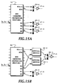
- Fig. 14A is a block diagram showing a third embodiment of the multiwavelength simultaneous monitoring circuit in accordance with the present invention.
- the outputs of the balanced photodetectors 25-0 and 25-i are inputted to the amplifiers 17-0 and 17-i.
- the output of the amplifier 17-0 is fed to the integrator 20-0, and the output of the integrator 20-0 is connected to the temperature control circuit 21 which controls the Peltier cooler 22 that regulates the temperature of the AWG 12.
- a configuration as shown in Fig. 15B may be adopted.
- the output waveguides #2 - #2n+1 are selectively connected to a combination of the balanced photodetector 25-1 and the amplifier 17-1 through optical switches 23-1 and 23-2.
- the present embodiment is characterized by carrying out the wavelength discrimination of the WDM signal while stabilizing the transmission characteristics of the AWG 12 by locking the crossover wavelength of the transmission characteristic curves of the output waveguides #0 and #1 to the reference wavelength ⁇ 0.
- the power of the reference optical signal takes a Gaussian distribution across the output waveguides #0 and #1 as shown in Fig. 16B.
- the Gaussian beam has overlaps with the output waveguides #0 and #1 as depicted by the shadowed portions.
- Figs. 17A and 17B are waveform diagrams illustrating the wavelength discrimination of the reference optical signal and the stabilization of the transmission characteristic in the third embodiment.
- the transmission characteristic of the output waveguides #0 and #1 takes one of the three states [1], [2] and [3] with respect to the reference wavelength ⁇ 0.
- the state [1] in which the transmission characteristic shifts to the long wavelength side with respect to the reference wavelength ⁇ 0, the light power associated with the output waveguide #0 grows stronger
- the state [3] in which the transmission characteristic shifts to the short wavelength side with respect to the reference wavelength ⁇ 0, the light power associated with the output waveguide #1 grow stronger.
- the state [2] in which the transmission characteristic coincides with the reference wavelength ⁇ 0, the light power is equally shared between the output waveguides #0 and #1.
- the signals Sa0 and Sa1 received by the balanced photodetector 25-0 connected to the output waveguides #0 and #1 vary in accordance with the states [1], [2] and [3]. Since the balanced photodetector 25-0 outputs the difference between the received signals Sa0 and Sa1 as an error signal Sc, it becomes a positive voltage in the state [3], a negative voltage in the state [1], and zero in the state [2].
- the error signal Sc undergoes time integration by the integrator 20-0, and is converted into the control signal Sd which controls the Peltier cooler 22. As a result, the feedback loop operates to lock the transmission characteristic of the AWG 12 to the reference wavelength ⁇ 0.
- the wavelength discrimination of the WDM signal is carried out in a similar manner. Specifically, since the transmission characteristics of the AWG 12 are stabilized to the reference wavelength ⁇ 0, the error signals outputted from the balanced photodetectors 25-1 - 25-n indicate the relative wavelength differences between the respective wavelengths ⁇ 1 - ⁇ n of the WDM signal and the transmission characteristics of the AWG 12.
- a combination of two photodetectors 16-1 and 16-2 connected to the two output waveguides and a differential amplifier 26 as shown in Fig. 14B may be used to handle the received signals, thus achieving similar effect and advantages.
- the wavelength errors are detected from the light power differences between the outputs of the two adjacent output waveguides of the AWG 12.
- the spacing between the adjacent output waveguides cannot be reduced to zero as shown in Fig. 16B, the light power component in the spacing between the output waveguides is not utilized. This will reduce the light power available for the photodetectors. In other words, the transmission power at the crossover wavelength will be reduced. This problem will be solved by the following configuration.
- Fig. 18 is a block diagram showing a fourth embodiment of the multiwavelength simultaneous monitoring circuit in accordance with the present invention.
- the reference optical signal R (wavelength ⁇ 0) and the WDM signal W (wavelengths ⁇ 1 - ⁇ n ) are multiplexed by a 2 ⁇ 2 optical coupler 27, and the multiplexed optical signal is injected into two input waveguides of the AWG 12.
- the multiplexed optical signal injected into a first input waveguide results in optical signals outputted from the output waveguides #0 - #n, whose wavelengths are ⁇ 0 and ⁇ 1 - ⁇ n .
- the multiplexed optical signal injected into a second input waveguide results in optical signals outputted from the output waveguides #n+1 - #2n+1, whose wavelengths are ⁇ 0 and ⁇ 1 - ⁇ n .
- Balanced photodetectors 25-0 and 25-i are each connected to two output waveguides associated with the same wavelengths as shown in Fig. 19A.
- the outputs of the balanced photodetectors 25-0 and 25-i are connected to the amplifiers 17-0 and 17-i, respectively.
- the output of the amplifier 17-0 is fed to the integrator 20-0, and the output of the integrator 20-0 is connected to the temperature control circuit 21, which controls the Peltier cooler 22 that regulates the temperature of the AWG 12.
- a configuration as shown in Fig. 19B may be adopted.
- the output waveguides #1 - #n and #n+2 - #2n+1 are selectively connected to a combination of the balanced photodetector 25-1 and the amplifier 17-1 through optical switches 23-1 and 23-2.
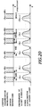
- the present embodiment is characterized in that the space between the output waveguides #0 - #n and the output waveguides #n+1 - #2n+1 is adjusted so that the two corresponding output waveguides are each associated with half of the light power of each wavelength as shown in Fig. 20.
- the output waveguide #0 is linked with half of the reference optical signal (wavelength ⁇ 0) on the short wavelength side
- the output waveguide #n+1 is linked with the other half of the reference optical signal (wavelength ⁇ 0) on the long wavelength side.
- the spacing between the output waveguides #n and #n+1 is set at 6 ⁇ as shown in Fig.
- the output waveguide #0 can be linked with half of the reference optical signal on the long wavelength side, and the output waveguide #n+1 can be linked with the other half of the reference optical signal on the short wavelength side.
- the wavelengths of the WDM signal are handled in a similar manner.
- the present embodiment is characterized in that the spacing between the output waveguides #n and #n+1 is set at 6 ⁇ , while all the other spacing of the output waveguides #0 - #n and #n+1 - #2n+1 are set at 4 ⁇ .
- the spacing between the output waveguide group I (#0 - #n) and the output waveguide group II (#n+1 - #2n+1) is made longer than the normal spacing 4 ⁇ by an amount of half the spacing 2 ⁇ , so that the interval between the two output waveguide groups I and II becomes 1.5 times the normal spacing (6 ⁇ ).
- the link with the output waveguide #0 reduces, whereas the link with the output waveguide #n+1 increases.
- the difference of the two is detected as in the third embodiment, and the Peltier cooler 22 is controlled in response to the difference.
- the feedback loop functions so as to keep the relative wavelength difference zero, and the transmission characteristics of the AWG 12 are stabilized to the reference wavelength ⁇ 0.
- the wavelength discrimination of the WDM signal is carried out in a similar manner. Specifically, since the transmission characteristics of the AWG 12 are stabilized to the reference wavelength ⁇ 0, the error signals outputted from the balanced photodetectors 25-1 - 25-n indicate the relative wavelength differences between the respective wavelengths ⁇ 1 - ⁇ n of the WDM signal and the transmission characteristics of the AWG 12.
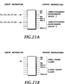
- a multiplexed optical signal of the reference optical signal R and the WDM signals W is injected into the input waveguides (a) and (b) as shown in Fig. 21A, so that a demultiplexed wavelength group I is produced from the output waveguides #0 - #n, and a demultiplexed wavelength group II is produced from the output waveguides #n+1 - #2n+1.
- the embodiment is not restricted to such a configuration.
- the zero-th order (diffraction order n) light signal is produced from the output waveguides #0 - #n
- the first order (diffraction order n+1) light signal is produced from the output waveguides #n+1 - #2n+1.
- the output power of the zero-th order light signal and that of the first order light signal must be matched by a differential amplifier 26 instead of the balanced photodetector before the wavelength discrimination.
- the spacings between the output waveguide groups of respective orders are set at 1.5 times the normal spacing (that is, 6 ⁇ ) of the WDM signal.
- the optical frequency discrimination can also be achieved.
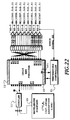
- Figs. 22 and 23 are block diagrams showing a fifth embodiment of the multiwavelength simultaneous monitoring circuit in accordance with the present invention.
- the fifth embodiment differs from the third embodiment shown in Fig. 14A in that the present embodiment obtains ratios between the outputs of two adjacent output ports rather than the differences between the two outputs as in the third embodiment.
- the outputs of a pair of photodetectors 16-ia and 16-ib are supplied to the first and second input terminals of logarithmic amplifiers 40-i, respectively.
- Each of the logarithmic amplifiers 40-i converts the two input signals into log values, followed by obtaining the difference between the two, thereby outputting the ratio of the outputs of the pair of adjacent output ports as the wavelength error signal.
- the AWG 12 of the present embodiment is a 16 ⁇ 16 AWG, and the wavelength spacing between the center transmission wavelengths of adjacent channels is 1 nm. Accordingly, FSR (Free Spectral Range) is 16 nm.
- the input ports are assigned to eight central input ports of the AWG 12.
- the center transmission wavelengths of respective channels of the AWG 12 vary in accordance with the position of an input port of the multiplexed light of the WDM signal and the reference optical signal.
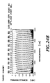
- Fig. 24A is a graph illustrating the transmission characteristics of the AWG 12 when the multiplexed wave of the WDM signal and the reference optical signal is injected into the input port #1 as shown in Fig. 22.
- the abscissas represent wavelengths, and the ordinates indicate transmittance.
- the output port number increments by one, the center transmission wavelength of respective channels shift by 1 nm toward longer wavelength side. For this reason, the output ports of increasing number are connected to longer wavelength side logarithmic amplifiers as shown in Fig. 22.
- the output ports #1 and #2 are connected to the first and second input terminals of a shortest wavelength side logarithmic amplifier 40-1 (output #G) through a pair of photodetectors 16-1a and 16-1b.
- the output ports #3 and #4 are connected to the first and second input terminals of a logarithmic amplifier 40-2 (output #F) through a pair of photodetectors 16-2a and 16-2b.
- Similar connections are repeated so that the output ports #13 and #14 are connected to the first and second input terminals of a longest wavelength side logarithmic amplifier 40-7 (output #A) through a pair of photodetectors 16-7a and 16-7b.
- the output ports #15 and #16 are for the reference optical signal, and connected to the first and second input terminals of a logarithmic amplifier 40-0 (output #H) through a pair of photodetectors 16-0a and 16-0b.
- Fig. 24B is a graph illustrating the transmission characteristics of the AWG 12 when the multiplexed wave of the WDM signal and the reference optical signal is injected into the input port #7 as shown in Fig. 23.
- the center transmission wavelengths of respective channels shift by 1 nm toward longer wavelength side.
- the center transmission wavelength of the output port #1 shifts by 6 nm toward the longer wavelength side, resulting in 1555 nm from 1549 nm.
- the output ports are connected as shown in Fig. 23.
- the output ports #1 and #2 are connected to the first and second input terminals of a logarithmic amplifier 40-4 (output #D), and the output ports #3 and #4 are connected to the first and second input terminals of a logarithmic amplifier 40-5 (output #C). Similar connections are repeated until the output ports #15 and #16 are connected to the first and second input terminals of a logarithmic amplifier 40-3 (output #E).
- the output ports #9 and #10 are connected to the first and second input terminals of the logarithmic amplifier 40-0 (output #H) for the reference optical signal.
- the input and output characteristics of the AWG 12 has periodic assignment.
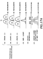
- the output from the output port #15 in Fig. 24A has center transmission wavelengths at 1547 nm and 1563 nm, which are separated apart by an amount of FSR (in this case, 16 nm). Similar effect is obtained for crossover wavelength which is defined as the intersection of two adjacent center transmission wavelength characteristic curves.
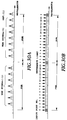
- Fig. 25 illustrates this.
- Fig. 25 (A) - (H) show the zero-cross points of the outputs #A - #H of the logarithmic amplifiers 40-7 - 40-0. As is clearly seen from this figure, the zero-cross points shift by 2 nm interval. This is because each logarithmic amplifier is connected to every two output ports.
- the wavelength error signal is obtained as a ratio of two output optical signals, high accuracy, stable wavelength discrimination can be achieved in spite of fluctuations in power of input optical signals.
- Figs. 26A and 26B are graphs comparatively illustrating the cases when the difference between the outputs from the two output ports are taken (Fig. 26A), and when the ratio between the two outputs are taken (Fig. 26B).
- the abscissas of the graphs represent normalized detuning from the crossover wavelengths, and the ordinates indicate the differences and ratios, which are normalized by input power.
- the difference output varies depending on the input light power P0 and P0/2
- the ratio output is independent of the input power, resulting in a constant characteristic.
- the range of measurement of the WDM signal is defined as a range in which the output of each logarithmic amplifier is established to produce the ratio of the two output optical signals. As shown in Fig. 26B, the output of each logarithmic amplifier becomes zero at the zero crossover wavelength, and increases as the wavelength separates apart from this point, and the range of measurement is limited to about 0.5 nm around the crossover wavelengths. In other words, the range of measurement corresponds to the linear portions about the crossover wavelengths such as 1547 - 1548 nm in Fig. 24(H).
- the wavelength of the reference optical signal can be set at a desired value in the output range of the logarithmic amplifier 40-0 (output #H). More specifically, adding to the wavelength error signal the offset corresponding to the difference between the set value of the crossover wavelength and the reference wavelength, which offset is outputted from the offset circuit 216 shown in Fig. 6, allows to use a reference wavelength different from the set crossover wavelength.
- the crossover wavelength of the AWG 12 is set at 1547.5 nm, whereas the reference wavelength outputted from the laser diode optical source 10 is 1547.485.
- the difference of 0.015 nm (1.8 GHz in terms of frequency) between the two can be adjusted on the output voltage offset of the logarithmic amplifier, so that stable control of the center transmission wavelength can be achieved.
- Fig. 27 is a block diagram showing a sixth embodiment of a multiwavelength simultaneous monitoring circuit in accordance with the present invention.
- the present embodiment differs from the fifth embodiment shown in Figs. 22 and 23 in that the WDM signal W and the reference optical signal R are injected into different input ports in the present embodiment. That is, the WDM signal W is inputted to the input port #5, whereas the reference optical signal R is inputted to the input port #7.
- the center transmission wavelengths of the WDM signal inputted to the input port #5 shift by 2 nm toward the shorter wavelength side than those of Fig. 23 where it is inputted to the input port #7. Accordingly, the respective crossover wavelengths also shift by 2 nm.
- the output #A of the logarithmic amplifier 40-7 shifts to 1559.5 nm when the input port is #5, from the crossover wavelength of 1561.5 when the input port is #7.
- the wavelength monitoring is possible even if one of the wavelength of the WDM signal W is the same as that of the reference optical signal R. This is because the two optical signals are outputted from different output ports although their wavelengths are the same.
- Figs. 28, 29, 30A and 30B are diagrams illustrating this.
- the wavelength allocation is as shown in Fig. 29 under the restriction that the number of output ports is twice the number of input wavelength, that is, one (for the reference optical signal) + the number of multiplexed wavelengths of the WDM signal.
- allowed wavelengths Ref(i) of the reference optical signal are limited to the wavelengths which are out of the wavelength range of the WDM signal, and integer multiples of the FSR.
- the reference optical signal in the ranges depicted by open squares in Fig. 30B are allowed against the WDM signal shown in Fig. 30A.
- the shaded squares in Fig. 30B indicate the reference wavelengths allowed when the WDM signal and the reference optical signals are inputted to the same input port.
- changing the input port of the reference optical signal R enables a desired wavelength to be used as the reference wavelength.
- the logarithmic amplifiers are employed for obtaining the ratios between the outputs of the AWG 12 in the fifth and sixth embodiments, the logarithmic amplifiers are not essential.
- A/D converters 41-0a - 41-07b, a DSP (Digital Signal Processor) 43, and D/A converters 45-0 - 45-7 can be used instead of the logarithmic amplifiers, resulting in similar effect and advantages.
- the input terminals of the A/D converters 41-0a - 41-7b are connected to the output terminals of photodetectors 16-0a - 16-7b, respectively.
- the D/A converters 45-0 - 45-7 can be obviated, in which case, the wavelength error signals are outputted in the form of digital signals.
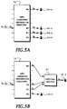
- Fig. 32 shows an embodiment, in which the multiwavelength simultaneous monitoring circuit in accordance with the present invention is applied to the wavelength control for laser diodes of a transmitter.
- optical signals with wavelengths of ⁇ 1 - ⁇ 7 outputted from laser diodes 51 - 57 are multiplexed by a multiplexer 91 to form a WDM signal which is supplied to an optical coupler 92.
- the optical coupler separates a part of the WDM signal, and supplies its fraction to a multiwavelength simultaneous monitoring circuit 93, and outputs the remainder thereof.
- the monitoring circuit 93 outputs differences ⁇ 1- ⁇ 01,..., ⁇ 7- ⁇ 07 between the predetermined wavelengths ⁇ 01, ..., ⁇ 07 and respective wavelength optical signals of the WDM signal.
- the differences are negatively fed back to injection current control circuits 61 - 67 of the laser diodes 51 - 57, so that the differences become zero.
- the oscillation wavelength of the laser diodes are stabilized at the set values ⁇ 01, ..., ⁇ 07.
- the injection current control circuits may be replaced by temperature control circuits to achieve the feedback control.
Landscapes
- Physics & Mathematics (AREA)
- Engineering & Computer Science (AREA)
- Microelectronics & Electronic Packaging (AREA)
- General Physics & Mathematics (AREA)
- Optics & Photonics (AREA)
- Electromagnetism (AREA)
- Computer Networks & Wireless Communication (AREA)
- Signal Processing (AREA)
- Optical Communication System (AREA)
- Optical Integrated Circuits (AREA)
Applications Claiming Priority (6)
| Application Number | Priority Date | Filing Date | Title |
|---|---|---|---|
| JP23002094 | 1994-09-26 | ||
| JP23002094 | 1994-09-26 | ||
| JP230020/94 | 1994-09-26 | ||
| JP2913/95 | 1995-01-11 | ||
| JP291395 | 1995-01-11 | ||
| JP291395 | 1995-01-11 |
Publications (3)
| Publication Number | Publication Date |
|---|---|
| EP0703679A2 true EP0703679A2 (fr) | 1996-03-27 |
| EP0703679A3 EP0703679A3 (fr) | 1999-12-15 |
| EP0703679B1 EP0703679B1 (fr) | 2004-04-28 |
Family
ID=26336408
Family Applications (1)
| Application Number | Title | Priority Date | Filing Date |
|---|---|---|---|
| EP95306741A Expired - Lifetime EP0703679B1 (fr) | 1994-09-26 | 1995-09-25 | Circuit de surveillance simultanée de plusieurs longueurs d'ondes utilisant un réseau de guides d'ondes groupés |
Country Status (3)
| Country | Link |
|---|---|
| US (1) | US5617234A (fr) |
| EP (1) | EP0703679B1 (fr) |
| DE (1) | DE69532941T2 (fr) |
Cited By (25)
| Publication number | Priority date | Publication date | Assignee | Title |
|---|---|---|---|---|
| EP0786879A2 (fr) * | 1996-01-25 | 1997-07-30 | Siemens Aktiengesellschaft | Méthode et circuit pour la stabilisation de fréquence d'un multiplexeur/démultiplexeur d'ondes |
| EP0798882A2 (fr) * | 1996-03-28 | 1997-10-01 | Lucent Technologies Inc. | Procédé et appareil de surveillance et connexion des paramètres de longueurs d'ondes individuelles dans un système multi-canal à multiplexage à division de longueur d'onde |
| EP0871343A2 (fr) * | 1997-04-09 | 1998-10-14 | TRW Inc. | Commutateur optique sans séparateurs avec capacité de diffusion |
| EP0978740A2 (fr) * | 1998-08-04 | 2000-02-09 | Nippon Telegraph and Telephone Corporation | Multiplexeur/démultiplexeur en longueur d'onde |
| FR2788596A1 (fr) * | 1999-01-14 | 2000-07-21 | Samsung Electronics Co Ltd | Module de dispositif a reseau de phase et dispositif pour surveiller un signal optique utilisant le module |
| US6118562A (en) * | 1997-05-16 | 2000-09-12 | Electronics And Telecommunications Research Institute | Wavelength aligning apparatus using arrayed waveguide grating |
| WO2000069103A2 (fr) * | 1999-04-23 | 2000-11-16 | Profile Optische Systeme Gmbh | Dispositif de controle des performances de systemes d-wdm multifrequence |
| WO2001023930A1 (fr) * | 1999-09-29 | 2001-04-05 | Koninklijke Philips Electronics N.V. | Dispositif optique pourvu d'un deuxieme guide d'ondes a reseau de diffraction en reseau permettant de commander la temperature |
| WO2001025849A2 (fr) * | 1999-09-23 | 2001-04-12 | Purdue Research Foundation | Conformateur direct d'impulsions espace-temps et generateur de trains d'impulsions optiques |
| FR2803115A1 (fr) * | 1999-12-28 | 2001-06-29 | Cit Alcatel | Dispositif de comparaison de longueur d'onde et de multiplexage et systeme de reglage de sources monochromatiques |
| WO2001058056A1 (fr) * | 2000-02-03 | 2001-08-09 | Bookham Technology Plc | Liaison optique point a point |
| WO2001059413A2 (fr) * | 2000-02-09 | 2001-08-16 | Infineon Technologies Ag | Procede et systeme pour mesurer des longueurs d'ondes optiques |
| FR2807526A1 (fr) * | 2000-04-10 | 2001-10-12 | Cit Alcatel | Dispositif et systeme de controle de longueur d'onde |
| GB2363536A (en) * | 2000-06-16 | 2001-12-19 | Ericsson Telefon Ab L M | WDM signal monitoring using variable arrayed waveguides |
| GB2375391A (en) * | 2001-05-09 | 2002-11-13 | Bookham Technology Plc | Measuring grid error in an optical device |
| WO2002099518A1 (fr) * | 2001-06-05 | 2002-12-12 | Bookham Technology Plc | Procede de mise en oeuvre d'un dispositif optique |
| WO2003024011A2 (fr) * | 2001-09-12 | 2003-03-20 | Lnl Optenia Inc. | Controleur de performance optique |
| GB2382937A (en) * | 2001-12-04 | 2003-06-11 | Marconi Optical Components Ltd | Wavelength control for a plurality of optical transmitters |
| DE10201125A1 (de) * | 2002-01-09 | 2003-07-24 | Infineon Technologies Ag | Interferometer und Anordnung zur Frequenzstabilisierung |
| WO2003079098A2 (fr) * | 2002-03-14 | 2003-09-25 | Intel Corporation | Boitier optique compact comprenant un connecteur optique modulaire |
| EP1396776A1 (fr) * | 2002-09-09 | 2004-03-10 | Samsung Electronics Co., Ltd. | Régulateur de température dans un appareil de communication optique et méthode correspondante |
| US6868200B2 (en) | 2001-08-06 | 2005-03-15 | Fujitsu Limited | Wavelength division multiplexing optical transmission apparatus |
| EP1608088A1 (fr) * | 2004-06-16 | 2005-12-21 | OpNext Japan, Inc. | Méthode et appareil pour transmettre un signal optique |
| US7272276B2 (en) | 2001-09-12 | 2007-09-18 | Enablence Inc. | Optical performance monitor |
| CN103217182A (zh) * | 2013-03-27 | 2013-07-24 | 黑龙江大学 | 一种基于滤色片的多通道光纤光栅解调装置 |
Families Citing this family (88)
| Publication number | Priority date | Publication date | Assignee | Title |
|---|---|---|---|---|
| JPH0964819A (ja) * | 1995-08-23 | 1997-03-07 | Fujitsu Ltd | 光システム |
| FR2743234B1 (fr) * | 1995-12-28 | 1998-01-23 | Alcatel Optronics | Demultiplexeur de longueurs d'onde |
| JP2858655B2 (ja) * | 1997-01-22 | 1999-02-17 | 日立電線株式会社 | 光波長合分波器 |
| US6304350B1 (en) * | 1997-05-27 | 2001-10-16 | Lucent Technologies Inc | Temperature compensated multi-channel, wavelength-division-multiplexed passive optical network |
| US5915052A (en) * | 1997-06-30 | 1999-06-22 | Uniphase Telecommunications Products, Inc. | Loop status monitor for determining the amplitude of the signal components of a multi-wavelength optical beam |
| US5850292A (en) * | 1997-11-13 | 1998-12-15 | Hewlett-Packard Company | Wavelength monitor for optical signals |
| US6023544A (en) * | 1997-12-24 | 2000-02-08 | Lucent Technologies Inc. | Monitoring with an optical wavelength router |
| US6441955B1 (en) * | 1998-02-27 | 2002-08-27 | Fujitsu Limited | Light wavelength-multiplexing systems |
| US6496300B2 (en) | 1998-02-27 | 2002-12-17 | Fujitsu Limited | Optical amplifier |
| KR100295810B1 (ko) | 1998-06-02 | 2001-10-26 | 서평원 | 파장분할다중방식광전송망채널감시시스템 |
| KR100318922B1 (ko) | 1998-07-30 | 2001-12-29 | 윤종용 | 파장 분할 다중방식을 채용한 광 전송시스템에서 안정화상태감시기능을 구비한 파장 안정화회로 |
| SE513095C2 (sv) * | 1998-10-02 | 2000-07-10 | Ericsson Telefon Ab L M | Förfarande och anordning för WDM-sändning och -mottagning |
| DE19845701A1 (de) * | 1998-10-05 | 2000-04-06 | Palme Dieter | Anordnungen zur Überwachung der Performance von DWDM-Mehrwellenlängensystemen |
| KR100319744B1 (ko) | 1998-11-09 | 2002-02-19 | 오길록 | 파장선택형광검출기를이용한파장분할다중화된광신호의채널정보검출장치및그방법 |
| KR100322124B1 (ko) | 1999-01-14 | 2002-02-04 | 윤종용 | 광신호 모니터링 장치 및 방법 |
| JP3434489B2 (ja) * | 1999-09-24 | 2003-08-11 | 古河電気工業株式会社 | アレイ導波路型回折格子 |
| JP2002071994A (ja) * | 1999-12-27 | 2002-03-12 | Furukawa Electric Co Ltd:The | アレイ導波路回折格子型光合分波器およびその製造方法 |
| EP1133082A1 (fr) * | 2000-03-10 | 2001-09-12 | Corning Incorporated | Système de controle optique |
| JP3829910B2 (ja) * | 2000-06-29 | 2006-10-04 | 横河電機株式会社 | 波長多重信号光の解析方法及びその装置 |
| US6298186B1 (en) * | 2000-07-07 | 2001-10-02 | Metrophotonics Inc. | Planar waveguide grating device and method having a passband with a flat-top and sharp-transitions |
| US7158722B1 (en) * | 2000-07-13 | 2007-01-02 | At&T Corp. | Method for operating transparent node for WDM shared “virtual ring” networks |
| US6807372B1 (en) * | 2000-07-14 | 2004-10-19 | University Of Maryland | Integrated spectral encoder/decoder for optical CDMA communication system |
| JP3679016B2 (ja) * | 2001-02-27 | 2005-08-03 | エヌティティエレクトロニクス株式会社 | 光合波回路、および、光合波装置 |
| US20020135840A1 (en) * | 2001-03-23 | 2002-09-26 | Robert Spagnoletti | Connection verification and monitoring in optical wavelength multiplexed communications systems |
| FR2822949B1 (fr) * | 2001-03-27 | 2004-01-09 | Commissariat Energie Atomique | Spectrometre optique integre a haute resolution spectrale, notamment pour les telecommunications a haut debit et la metrologie, et procede de fabrication |
| US6594409B2 (en) | 2001-04-18 | 2003-07-15 | Apic Corporation | WDM transmitter or receiver including an array waveguide grating and active optical elements |
| US7495765B2 (en) * | 2001-05-17 | 2009-02-24 | Thorlabs Gmbh | Fiber polarimeter, the use thereof, as well as polarimetric method |
| EP1262752B1 (fr) * | 2001-05-17 | 2005-08-03 | THORLABS GmbH | Polarimètre à fibre, son utilisation, ainsi qu'une méthode polarimétrique |
| WO2003025634A2 (fr) * | 2001-08-27 | 2003-03-27 | Rensselaer Polytechnic Institute | Differentiateur de terahertz dans le domaine temps |
| US20060139755A1 (en) * | 2001-08-27 | 2006-06-29 | Roland Kersting | Terahertz time-domain differentiator |
| US7751658B2 (en) * | 2001-10-09 | 2010-07-06 | Infinera Corporation | Monolithic transmitter photonic integrated circuit (TxPIC) having tunable modulated sources with feedback system for source power level or wavelength tuning |
| CA2463500C (fr) * | 2001-10-09 | 2012-11-27 | Infinera Corporation | Architectures et systemes de commande de microcircuits integres photoniques d'emission (txpic) et stabilisation de longueurs d'ondes pour txpics |
| US20080044128A1 (en) * | 2001-10-09 | 2008-02-21 | Infinera Corporation | TRANSMITTER PHOTONIC INTEGRATED CIRCUITS (TxPICs) AND OPTICAL TRANSPORT NETWORK SYSTEM EMPLOYING TxPICs |
| US7116851B2 (en) * | 2001-10-09 | 2006-10-03 | Infinera Corporation | Optical signal receiver, an associated photonic integrated circuit (RxPIC), and method improving performance |
| US7672546B2 (en) * | 2001-10-09 | 2010-03-02 | Infinera Corporation | Optical transport network having a plurality of monolithic photonic integrated circuit semiconductor chips |
| AU2002334906A1 (en) * | 2001-10-09 | 2003-04-22 | Infinera Corporation | Transmitter photonic integrated circuits (txpic) and optical transport networks employing txpics |
| US6597841B1 (en) | 2002-01-14 | 2003-07-22 | Corning Incorporated | Multi-output arrayed waveguide grating demultiplexer |
| AU2002364229A1 (en) * | 2002-01-16 | 2003-09-02 | Teraphase Technologies, Inc. | System and method of transmitting optical signals |
| US6768827B2 (en) * | 2002-01-16 | 2004-07-27 | The Regents Of The University Of California | Integrated optical router |
| US6801183B2 (en) * | 2002-04-10 | 2004-10-05 | Lightwaves 2020, Inc. | Temperature compensation for liquid crystal cell optical devices |
| US7149425B2 (en) * | 2002-04-30 | 2006-12-12 | Lucent Technologies Inc. | Monitoring system for an optical transmitter |
| US6876784B2 (en) * | 2002-05-30 | 2005-04-05 | Nanoopto Corporation | Optical polarization beam combiner/splitter |
| US7386205B2 (en) * | 2002-06-17 | 2008-06-10 | Jian Wang | Optical device and method for making same |
| US7283571B2 (en) * | 2002-06-17 | 2007-10-16 | Jian Wang | Method and system for performing wavelength locking of an optical transmission source |
| US20040047039A1 (en) * | 2002-06-17 | 2004-03-11 | Jian Wang | Wide angle optical device and method for making same |
| EP1520203A4 (fr) | 2002-06-18 | 2005-08-24 | Nanoopto Corp | Composants optiques presentant une meilleure fonctionnalite et leur procede de fabrication |
| JP2005534981A (ja) | 2002-08-01 | 2005-11-17 | ナノオプト コーポレーション | 精密位相遅れ装置およびそれを製造する方法 |
| US7747114B2 (en) * | 2002-10-08 | 2010-06-29 | Infinera Corporation | Tilted combiners/decombiners and photonic integrated circuits (PICs) employing the same |
| US7013064B2 (en) * | 2002-10-09 | 2006-03-14 | Nanoopto Corporation | Freespace tunable optoelectronic device and method |
| US6920272B2 (en) * | 2002-10-09 | 2005-07-19 | Nanoopto Corporation | Monolithic tunable lasers and reflectors |
| US6915030B2 (en) * | 2002-11-15 | 2005-07-05 | Mikelis Nils Svilans | Optical spectrum analyzer |
| US7268946B2 (en) * | 2003-02-10 | 2007-09-11 | Jian Wang | Universal broadband polarizer, devices incorporating same, and method of making same |
| US7139455B1 (en) * | 2003-03-18 | 2006-11-21 | Luxtera | Electronically controllable arrayed waveguide gratings |
| US20040258355A1 (en) * | 2003-06-17 | 2004-12-23 | Jian Wang | Micro-structure induced birefringent waveguiding devices and methods of making same |
| US7130505B2 (en) * | 2003-07-23 | 2006-10-31 | Jds Uniphase Corporation | Optical performance monitor |
| US7035505B2 (en) * | 2003-07-23 | 2006-04-25 | Jds Uniphase Corporation | Optical performance monitor |
| US7603045B2 (en) * | 2003-08-28 | 2009-10-13 | Fujitsu Limited | Method and system for automatic feedback control for fine tuning a delay interferometer |
| WO2005106546A2 (fr) * | 2004-04-15 | 2005-11-10 | Infinera Corporation | Circuits photoniques integres a grille de longueurs d'onde flottante sans refroidisseur pour reseaux a transmission par multiplexage par repartition en longueur d'onde |
| US20060188255A1 (en) * | 2005-02-18 | 2006-08-24 | Fujitsu Limited | Monitoring wavelength dispersion variation using photon absorption |
| JP2006270283A (ja) * | 2005-03-23 | 2006-10-05 | Fujitsu Ltd | 多波長光源を用いた波長分割多重伝送装置 |
| US7701988B2 (en) * | 2005-04-20 | 2010-04-20 | Finisar Corporation | Optical transmit assembly including thermally isolated laser, temperature sensor, and temperature driver |
| DE102005045286A1 (de) * | 2005-09-22 | 2007-04-12 | Fraunhofer-Gesellschaft zur Förderung der angewandten Forschung e.V. | Wellenleiter-integrierte Photodiode |
| JP4816969B2 (ja) | 2005-10-05 | 2011-11-16 | 日本電気株式会社 | 光受信器、光通信システム及び方法 |
| JP4892262B2 (ja) * | 2006-03-23 | 2012-03-07 | 富士通株式会社 | 光源波長制御装置 |
| US8285150B2 (en) * | 2006-10-02 | 2012-10-09 | Futurewei Technologies, Inc. | Method and system for integrated DWDM transmitters |
| US8285149B2 (en) * | 2006-10-02 | 2012-10-09 | Futurewei Technologies, Inc. | Method and system for integrated DWDM transmitters |
| US7532783B2 (en) * | 2006-10-11 | 2009-05-12 | Futurewei Technologies, Inc. | Method and system for integrated DWDM receivers |
| US8050525B2 (en) * | 2006-10-11 | 2011-11-01 | Futurewei Technologies, Inc. | Method and system for grating taps for monitoring a DWDM transmitter array integrated on a PLC platform |
| US8285151B2 (en) * | 2006-10-20 | 2012-10-09 | Futurewei Technologies, Inc. | Method and system for hybrid integrated 1XN DWDM transmitter |
| JP4920489B2 (ja) * | 2007-05-16 | 2012-04-18 | 株式会社日立製作所 | 光分岐挿入装置 |
| US7852475B2 (en) * | 2007-08-13 | 2010-12-14 | Jds Uniphase Corporation | Scanning spectrometer with multiple photodetectors |
| US7832944B2 (en) | 2007-11-08 | 2010-11-16 | Finisar Corporation | Optoelectronic subassembly with integral thermoelectric cooler driver |
| US9438004B2 (en) * | 2011-05-20 | 2016-09-06 | Alcatel Lucent | Optical pumping and powering in spatially multiplexed transmission links |
| US9341774B2 (en) * | 2012-01-24 | 2016-05-17 | Applied Optoelectronics, Inc. | Optically matched laser array coupling assembly for coupling laser array to arrayed waveguide grating |
| US8805187B2 (en) * | 2012-03-19 | 2014-08-12 | Neophotonics Corporation | Wavelength router with feedback control comprising optical monitor ports |
| US9525490B2 (en) * | 2012-07-26 | 2016-12-20 | Aurrion, Inc. | Reconfigurable optical transmitter |
| US9285538B2 (en) * | 2012-10-23 | 2016-03-15 | Lumentum Operations Llc | Reducing temperature drift of an arrayed waveguide grating |
| US9207399B2 (en) * | 2013-01-28 | 2015-12-08 | Aurrion, Inc. | Athermal optical filter with active tuning and simplified control |
| AU2014235949B2 (en) | 2013-03-20 | 2017-09-07 | Nistica, Inc. | Wavelength selective switch having integrated channel monitor |
| US9755738B2 (en) * | 2013-03-20 | 2017-09-05 | Nistica, Inc. | Crosstalk suppression in a multi-photodetector optical channel monitor |
| JP6341601B2 (ja) * | 2014-04-01 | 2018-06-13 | 国立研究開発法人情報通信研究機構 | 波長多重分離器とそれを用いた波長多重器 |
| KR102644439B1 (ko) * | 2015-07-17 | 2024-03-07 | 트리나미엑스 게엠베하 | 하나 이상의 물체를 광학적으로 검출하기 위한 검출기 |
| CN111273395B (zh) | 2015-07-24 | 2021-11-16 | 瞻博网络公司 | 波导阵列中的相位调谐 |
| US10042116B2 (en) * | 2016-04-25 | 2018-08-07 | Applied Optoelectronics, Inc. | Techniques for direct optical coupling of photodetectors to optical demultiplexer outputs and an optical transceiver using the same |
| CN105866904A (zh) | 2016-05-23 | 2016-08-17 | 宁波环球广电科技有限公司 | 多通道并行的光接收器件 |
| CN206920661U (zh) | 2017-07-13 | 2018-01-23 | 宁波环球广电科技有限公司 | 高速光收发模块 |
| US10979167B2 (en) * | 2018-10-01 | 2021-04-13 | Huawei Technologies Co., Ltd. | Systems and method of multi-laser wavelength control |
| US11835760B1 (en) * | 2022-06-17 | 2023-12-05 | Taiwan Semiconductor Manufacturing Company Ltd. | Calibration system for wavelength-division multiplexing, wavelength-division multiplexing system, and calibrating method for wavelength-division multiplexing |
Citations (3)
| Publication number | Priority date | Publication date | Assignee | Title |
|---|---|---|---|---|
| EP0336308A2 (fr) * | 1988-03-31 | 1989-10-11 | CSELT Centro Studi e Laboratori Telecomunicazioni S.p.A. | Méthode et dispositif pour la régulation automatique de la fréquence des lasers à semi-conducteur |
| EP0481242A2 (fr) * | 1990-09-20 | 1992-04-22 | Fujitsu Limited | Dispositif pour contrôler et mesurer le balayage de la fréquence optique d'un laser |
| EP0613263A1 (fr) * | 1993-02-24 | 1994-08-31 | AT&T Corp. | Réseau optique comportant un démultiplexeur de longueur d'onde compact |
Family Cites Families (9)
| Publication number | Priority date | Publication date | Assignee | Title |
|---|---|---|---|---|
| JPH0738614B2 (ja) * | 1988-08-01 | 1995-04-26 | 日本電信電話株式会社 | 光fsk光周波数偏移安定化回路 |
| JPH0752271B2 (ja) * | 1989-06-19 | 1995-06-05 | 日本電信電話株式会社 | 光周波数安定化装置 |
| JPH0738615B2 (ja) * | 1989-08-21 | 1995-04-26 | 日本電信電話株式会社 | 光fsk周波数偏移安定化回路 |
| JPH0595153A (ja) * | 1991-10-01 | 1993-04-16 | Nippon Telegr & Teleph Corp <Ntt> | 光fsk周波数偏移安定化回路 |
| JP3256713B2 (ja) * | 1992-06-27 | 2002-02-12 | キヤノン株式会社 | 波長可変フィルタ制御方式、制御装置及びそれを用いた光通信システム |
| EP0591042B1 (fr) * | 1992-09-29 | 1997-05-28 | Nippon Telegraph And Telephone Corporation | Multi/Démultiplexeur avec réseau de guides d'ondes groupés et chemins optiques bouclés en retour |
| JP2546151B2 (ja) * | 1993-06-15 | 1996-10-23 | 日本電気株式会社 | レーザダイオード発光波長制御装置 |
| DE69421579T2 (de) * | 1993-08-02 | 2000-06-21 | Nippon Telegraph & Telephone | Integrierter optischer Wellenleiter-Schaltkreis und Test-System für verzweigte optische Leitungen, die ihn benutzen |
| US5532864A (en) * | 1995-06-01 | 1996-07-02 | Ciena Corporation | Optical monitoring channel for wavelength division multiplexed optical communication system |
-
1995
- 1995-09-21 US US08/531,980 patent/US5617234A/en not_active Expired - Fee Related
- 1995-09-25 DE DE69532941T patent/DE69532941T2/de not_active Expired - Fee Related
- 1995-09-25 EP EP95306741A patent/EP0703679B1/fr not_active Expired - Lifetime
Patent Citations (3)
| Publication number | Priority date | Publication date | Assignee | Title |
|---|---|---|---|---|
| EP0336308A2 (fr) * | 1988-03-31 | 1989-10-11 | CSELT Centro Studi e Laboratori Telecomunicazioni S.p.A. | Méthode et dispositif pour la régulation automatique de la fréquence des lasers à semi-conducteur |
| EP0481242A2 (fr) * | 1990-09-20 | 1992-04-22 | Fujitsu Limited | Dispositif pour contrôler et mesurer le balayage de la fréquence optique d'un laser |
| EP0613263A1 (fr) * | 1993-02-24 | 1994-08-31 | AT&T Corp. | Réseau optique comportant un démultiplexeur de longueur d'onde compact |
Non-Patent Citations (2)
| Title |
|---|
| JIANG Q ET AL: "FREQUENCY STABILISATION OF FDM OPTICAL SIGNALS BY TIME DIVISION MULTIPLEXING" ELECTRONICS LETTERS, vol. 25, no. 24, 23 November 1989 (1989-11-23), pages 1626-1628, XP000081481 ISSN: 0013-5194 * |
| MEISSNER P ET AL: "EXPERIMENTALSYSTEME FUER ZUKUENFTIGE KOHAERENTE OPTISCHE TV -VERTEIL- UND BIDIREKTIONALE KOMMUNIKATIONSSYSTEME" NACHRICHTENTECHNIK ELEKTRONIK, vol. 42, no. 5, 1 September 1992 (1992-09-01), pages 171-174, XP000310195 ISSN: 0323-4657 * |
Cited By (52)
| Publication number | Priority date | Publication date | Assignee | Title |
|---|---|---|---|---|
| EP0786879A3 (fr) * | 1996-01-25 | 2000-01-05 | Siemens Aktiengesellschaft | Méthode et circuit pour la stabilisation de fréquence d'un multiplexeur/démultiplexeur d'ondes |
| EP0786879A2 (fr) * | 1996-01-25 | 1997-07-30 | Siemens Aktiengesellschaft | Méthode et circuit pour la stabilisation de fréquence d'un multiplexeur/démultiplexeur d'ondes |
| EP0798882A3 (fr) * | 1996-03-28 | 2001-11-07 | Lucent Technologies Inc. | Procédé et appareil de surveillance et connexion des paramètres de longueurs d'ondes individuelles dans un système multi-canal à multiplexage à division de longueur d'onde |
| EP0798882A2 (fr) * | 1996-03-28 | 1997-10-01 | Lucent Technologies Inc. | Procédé et appareil de surveillance et connexion des paramètres de longueurs d'ondes individuelles dans un système multi-canal à multiplexage à division de longueur d'onde |
| EP0871343A2 (fr) * | 1997-04-09 | 1998-10-14 | TRW Inc. | Commutateur optique sans séparateurs avec capacité de diffusion |
| EP0871343A3 (fr) * | 1997-04-09 | 2006-11-15 | Northrop Grumman Corporation | Commutateur optique sans séparateurs avec capacité de diffusion |
| US6118562A (en) * | 1997-05-16 | 2000-09-12 | Electronics And Telecommunications Research Institute | Wavelength aligning apparatus using arrayed waveguide grating |
| EP0978740A3 (fr) * | 1998-08-04 | 2003-07-02 | Nippon Telegraph and Telephone Corporation | Multiplexeur/démultiplexeur en longueur d'onde |
| EP0978740A2 (fr) * | 1998-08-04 | 2000-02-09 | Nippon Telegraph and Telephone Corporation | Multiplexeur/démultiplexeur en longueur d'onde |
| GB2346024A (en) * | 1999-01-14 | 2000-07-26 | Samsung Electronics Co Ltd | Arrayed waveguide grating (AWG) module for monitoring optical signals |
| US6701042B1 (en) | 1999-01-14 | 2004-03-02 | Samsung Electronics Co., Ltd. | Arrayed waveguide grating module and device and method for monitoring optical signal using the same |
| GB2346024B (en) * | 1999-01-14 | 2001-04-11 | Samsung Electronics Co Ltd | Device for monitoring optical signal using an arrayed waveguide grating module |
| FR2788596A1 (fr) * | 1999-01-14 | 2000-07-21 | Samsung Electronics Co Ltd | Module de dispositif a reseau de phase et dispositif pour surveiller un signal optique utilisant le module |
| WO2000069103A3 (fr) * | 1999-04-23 | 2001-04-12 | Profile Optische Systeme Gmbh | Dispositif de controle des performances de systemes d-wdm multifrequence |
| WO2000069103A2 (fr) * | 1999-04-23 | 2000-11-16 | Profile Optische Systeme Gmbh | Dispositif de controle des performances de systemes d-wdm multifrequence |
| US6577782B1 (en) | 1999-09-23 | 2003-06-10 | Purdue Research Foundation | Direct space-to-time pulse shaper and optical pulse train generator |
| WO2001025849A3 (fr) * | 1999-09-23 | 2001-10-11 | Purdue Research Foundation | Conformateur direct d'impulsions espace-temps et generateur de trains d'impulsions optiques |
| WO2001025849A2 (fr) * | 1999-09-23 | 2001-04-12 | Purdue Research Foundation | Conformateur direct d'impulsions espace-temps et generateur de trains d'impulsions optiques |
| WO2001023930A1 (fr) * | 1999-09-29 | 2001-04-05 | Koninklijke Philips Electronics N.V. | Dispositif optique pourvu d'un deuxieme guide d'ondes a reseau de diffraction en reseau permettant de commander la temperature |
| US6477294B1 (en) | 1999-09-29 | 2002-11-05 | Koninklijke Philips Electronics N.V. | Optical device having second arrayed waveguide grating for temperature control |
| FR2803115A1 (fr) * | 1999-12-28 | 2001-06-29 | Cit Alcatel | Dispositif de comparaison de longueur d'onde et de multiplexage et systeme de reglage de sources monochromatiques |
| EP1113595A1 (fr) * | 1999-12-28 | 2001-07-04 | Alcatel | Dispositif de comparaison de longueur d'onde et de multiplexage et système de réglage de sources monochromatiques |
| US6690859B2 (en) | 1999-12-28 | 2004-02-10 | Avanex Corporation | Device for comparing wavelength values and multiplexing and a system for monitoring monochromatic sources |
| WO2001058056A1 (fr) * | 2000-02-03 | 2001-08-09 | Bookham Technology Plc | Liaison optique point a point |
| WO2001059413A3 (fr) * | 2000-02-09 | 2002-03-14 | Infineon Technologies Ag | Procede et systeme pour mesurer des longueurs d'ondes optiques |
| WO2001059413A2 (fr) * | 2000-02-09 | 2001-08-16 | Infineon Technologies Ag | Procede et systeme pour mesurer des longueurs d'ondes optiques |
| EP1146363A1 (fr) * | 2000-04-10 | 2001-10-17 | Alcatel | Dispositif et système de contrôle de longeur d'onde |
| FR2807526A1 (fr) * | 2000-04-10 | 2001-10-12 | Cit Alcatel | Dispositif et systeme de controle de longueur d'onde |
| US6516119B2 (en) | 2000-04-10 | 2003-02-04 | Alcatel | Device and system for wavelength monitoring |
| GB2363536B (en) * | 2000-06-16 | 2004-03-24 | Ericsson Telefon Ab L M | WDM signal monitoring |
| GB2363536A (en) * | 2000-06-16 | 2001-12-19 | Ericsson Telefon Ab L M | WDM signal monitoring using variable arrayed waveguides |
| WO2001097424A1 (fr) * | 2000-06-16 | 2001-12-20 | Telefonaktiebolaget Lm Ericsson (Publ) | Surveillance de signal mrl |
| WO2002091052A1 (fr) * | 2001-05-09 | 2002-11-14 | Bookham Technology Plc | Calage de grille dans un dispositif optique |
| GB2375391A (en) * | 2001-05-09 | 2002-11-13 | Bookham Technology Plc | Measuring grid error in an optical device |
| WO2002099518A1 (fr) * | 2001-06-05 | 2002-12-12 | Bookham Technology Plc | Procede de mise en oeuvre d'un dispositif optique |
| US6868200B2 (en) | 2001-08-06 | 2005-03-15 | Fujitsu Limited | Wavelength division multiplexing optical transmission apparatus |
| WO2003024011A3 (fr) * | 2001-09-12 | 2003-12-11 | Lnl Optenia Inc | Controleur de performance optique |
| WO2003024011A2 (fr) * | 2001-09-12 | 2003-03-20 | Lnl Optenia Inc. | Controleur de performance optique |
| US7272276B2 (en) | 2001-09-12 | 2007-09-18 | Enablence Inc. | Optical performance monitor |
| GB2382937A (en) * | 2001-12-04 | 2003-06-11 | Marconi Optical Components Ltd | Wavelength control for a plurality of optical transmitters |
| DE10201125A1 (de) * | 2002-01-09 | 2003-07-24 | Infineon Technologies Ag | Interferometer und Anordnung zur Frequenzstabilisierung |
| DE10201125C2 (de) * | 2002-01-09 | 2003-12-18 | Infineon Technologies Ag | Anordnung zur Frequenzstabilisierung |
| CN100388031C (zh) * | 2002-03-14 | 2008-05-14 | 英特尔公司 | 具有模块化光连接器的紧凑型光学封装件 |
| WO2003079098A2 (fr) * | 2002-03-14 | 2003-09-25 | Intel Corporation | Boitier optique compact comprenant un connecteur optique modulaire |
| US6860642B2 (en) | 2002-03-14 | 2005-03-01 | Intel Corporation | Compact optical package with modular optical connector |
| JP2006508373A (ja) * | 2002-03-14 | 2006-03-09 | インテル・コーポレーション | モジュール方式光コネクタを備えるコンパクトな光学パッケージ |
| WO2003079098A3 (fr) * | 2002-03-14 | 2006-04-06 | Intel Corp | Boitier optique compact comprenant un connecteur optique modulaire |
| US7031356B2 (en) | 2002-09-09 | 2006-04-18 | Samsung Electronics Co Ltd | Temperature controller in optical communication device and method for same |
| EP1396776A1 (fr) * | 2002-09-09 | 2004-03-10 | Samsung Electronics Co., Ltd. | Régulateur de température dans un appareil de communication optique et méthode correspondante |
| EP1608088A1 (fr) * | 2004-06-16 | 2005-12-21 | OpNext Japan, Inc. | Méthode et appareil pour transmettre un signal optique |
| CN103217182A (zh) * | 2013-03-27 | 2013-07-24 | 黑龙江大学 | 一种基于滤色片的多通道光纤光栅解调装置 |
| CN103217182B (zh) * | 2013-03-27 | 2015-05-20 | 黑龙江大学 | 一种基于滤色片的多通道光纤光栅解调装置 |
Also Published As
| Publication number | Publication date |
|---|---|
| EP0703679A3 (fr) | 1999-12-15 |
| DE69532941D1 (de) | 2004-06-03 |
| DE69532941T2 (de) | 2005-06-09 |
| US5617234A (en) | 1997-04-01 |
| EP0703679B1 (fr) | 2004-04-28 |
Similar Documents
| Publication | Publication Date | Title |
|---|---|---|
| EP0703679B1 (fr) | Circuit de surveillance simultanée de plusieurs longueurs d'ondes utilisant un réseau de guides d'ondes groupés | |
| US6240109B1 (en) | Wavelength stabilization of wavelength division multiplexed channels | |
| US7023887B2 (en) | Method and system for controlling optical wavelength based on optical frequency pulling | |
| US6891149B1 (en) | Optical phase detector | |
| US6782017B1 (en) | Wavelength locker and wavelength discriminating apparatus | |
| US6717967B2 (en) | Absolutely calibrated periodic filters and sources | |
| US6862303B2 (en) | Multiwavelength locking method and apparatus using acousto-optic tunable filter | |
| JP3902373B2 (ja) | 安定波長光通信用自己監視型光源 | |
| US7061610B2 (en) | Photonic integrated circuit based planar wavelength meter | |
| US7274870B2 (en) | Apparatus and method for simultaneous channel and optical signal-to-noise ratio monitoring | |
| JP3189199B2 (ja) | 波長監視装置 | |
| US6493125B1 (en) | Apparatus for stabilizing light source frequency | |
| US20020181062A1 (en) | Optical signal generator with stabilized carrier frequency output | |
| US6587278B1 (en) | Optical interferometer and signal synthesizer using the interferometer | |
| GB2455400A (en) | Wavelength meter and associated method | |
| US6724786B2 (en) | Variable optical attenuator using wavelength locked loop tuning | |
| WO2002039553A2 (fr) | Dispositif de verrouillage de longueurs d'onde | |
| US6927377B2 (en) | Wavelength locking channel monitor | |
| JPH09252283A (ja) | 波長監視装置 | |
| JPH10209973A (ja) | 光波長多重送信回路 | |
| WO2001097424A1 (fr) | Surveillance de signal mrl | |
| US20230198227A1 (en) | Opto-electronic system and method | |
| JPH0897775A (ja) | 波長監視装置 | |
| JP2939840B2 (ja) | 光波長可変フィルタ制御方法及び装置 | |
| EP1485976A2 (fr) | Sources et filtres periodiques a etalonnage absolu |
Legal Events
| Date | Code | Title | Description |
|---|---|---|---|
| PUAI | Public reference made under article 153(3) epc to a published international application that has entered the european phase |
Free format text: ORIGINAL CODE: 0009012 |
|
| 17P | Request for examination filed |
Effective date: 19951009 |
|
| AK | Designated contracting states |
Kind code of ref document: A2 Designated state(s): DE FR GB |
|
| PUAL | Search report despatched |
Free format text: ORIGINAL CODE: 0009013 |
|
| AK | Designated contracting states |
Kind code of ref document: A3 Designated state(s): DE FR GB |
|
| RIC1 | Information provided on ipc code assigned before grant |
Free format text: 6H 04B 10/14 A, 6H 04J 14/02 B, 6H 01S 3/133 B |
|
| GRAP | Despatch of communication of intention to grant a patent |
Free format text: ORIGINAL CODE: EPIDOSNIGR1 |
|
| GRAS | Grant fee paid |
Free format text: ORIGINAL CODE: EPIDOSNIGR3 |
|
| GRAA | (expected) grant |
Free format text: ORIGINAL CODE: 0009210 |
|
| RIC1 | Information provided on ipc code assigned before grant |
Ipc: 7H 01S 3/13 B Ipc: 7H 04J 14/02 B Ipc: 7H 04B 10/14 A |
|
| AK | Designated contracting states |
Kind code of ref document: B1 Designated state(s): DE FR GB |
|
| REG | Reference to a national code |
Ref country code: GB Ref legal event code: FG4D |
|
| RIC1 | Information provided on ipc code assigned before grant |
Ipc: 7H 01S 5/068 B Ipc: 7H 04J 14/02 B Ipc: 7H 04B 10/14 A |
|
| REF | Corresponds to: |
Ref document number: 69532941 Country of ref document: DE Date of ref document: 20040603 Kind code of ref document: P |
|
| ET | Fr: translation filed | ||
| PLBE | No opposition filed within time limit |
Free format text: ORIGINAL CODE: 0009261 |
|
| STAA | Information on the status of an ep patent application or granted ep patent |
Free format text: STATUS: NO OPPOSITION FILED WITHIN TIME LIMIT |
|
| 26N | No opposition filed |
Effective date: 20050131 |
|
| PGFP | Annual fee paid to national office [announced via postgrant information from national office to epo] |
Ref country code: FR Payment date: 20050823 Year of fee payment: 11 |
|
| PGFP | Annual fee paid to national office [announced via postgrant information from national office to epo] |
Ref country code: GB Payment date: 20050921 Year of fee payment: 11 |
|
| PGFP | Annual fee paid to national office [announced via postgrant information from national office to epo] |
Ref country code: DE Payment date: 20050922 Year of fee payment: 11 |
|
| PG25 | Lapsed in a contracting state [announced via postgrant information from national office to epo] |
Ref country code: DE Free format text: LAPSE BECAUSE OF NON-PAYMENT OF DUE FEES Effective date: 20070403 |
|
| GBPC | Gb: european patent ceased through non-payment of renewal fee |
Effective date: 20060925 |
|
| REG | Reference to a national code |
Ref country code: FR Ref legal event code: ST Effective date: 20070531 |
|
| PG25 | Lapsed in a contracting state [announced via postgrant information from national office to epo] |
Ref country code: GB Free format text: LAPSE BECAUSE OF NON-PAYMENT OF DUE FEES Effective date: 20060925 |
|
| PG25 | Lapsed in a contracting state [announced via postgrant information from national office to epo] |
Ref country code: FR Free format text: LAPSE BECAUSE OF NON-PAYMENT OF DUE FEES Effective date: 20061002 |