EP0703545B1 - Optisches Aufzeichnungsmedium - Google Patents
Optisches Aufzeichnungsmedium Download PDFInfo
- Publication number
- EP0703545B1 EP0703545B1 EP19950306645 EP95306645A EP0703545B1 EP 0703545 B1 EP0703545 B1 EP 0703545B1 EP 19950306645 EP19950306645 EP 19950306645 EP 95306645 A EP95306645 A EP 95306645A EP 0703545 B1 EP0703545 B1 EP 0703545B1
- Authority
- EP
- European Patent Office
- Prior art keywords
- layer
- optical recording
- recording medium
- transparent protective
- medium according
- Prior art date
- Legal status (The legal status is an assumption and is not a legal conclusion. Google has not performed a legal analysis and makes no representation as to the accuracy of the status listed.)
- Expired - Lifetime
Links
Images


Classifications
-
- G—PHYSICS
- G06—COMPUTING OR CALCULATING; COUNTING
- G06K—GRAPHICAL DATA READING; PRESENTATION OF DATA; RECORD CARRIERS; HANDLING RECORD CARRIERS
- G06K19/00—Record carriers for use with machines and with at least a part designed to carry digital markings
- G06K19/06—Record carriers for use with machines and with at least a part designed to carry digital markings characterised by the kind of the digital marking, e.g. shape, nature, code
- G06K19/06009—Record carriers for use with machines and with at least a part designed to carry digital markings characterised by the kind of the digital marking, e.g. shape, nature, code with optically detectable marking
- G06K19/06046—Constructional details
-
- Y—GENERAL TAGGING OF NEW TECHNOLOGICAL DEVELOPMENTS; GENERAL TAGGING OF CROSS-SECTIONAL TECHNOLOGIES SPANNING OVER SEVERAL SECTIONS OF THE IPC; TECHNICAL SUBJECTS COVERED BY FORMER USPC CROSS-REFERENCE ART COLLECTIONS [XRACs] AND DIGESTS
- Y10—TECHNICAL SUBJECTS COVERED BY FORMER USPC
- Y10T—TECHNICAL SUBJECTS COVERED BY FORMER US CLASSIFICATION
- Y10T428/00—Stock material or miscellaneous articles
- Y10T428/24—Structurally defined web or sheet [e.g., overall dimension, etc.]
- Y10T428/24942—Structurally defined web or sheet [e.g., overall dimension, etc.] including components having same physical characteristic in differing degree
-
- Y—GENERAL TAGGING OF NEW TECHNOLOGICAL DEVELOPMENTS; GENERAL TAGGING OF CROSS-SECTIONAL TECHNOLOGIES SPANNING OVER SEVERAL SECTIONS OF THE IPC; TECHNICAL SUBJECTS COVERED BY FORMER USPC CROSS-REFERENCE ART COLLECTIONS [XRACs] AND DIGESTS
- Y10—TECHNICAL SUBJECTS COVERED BY FORMER USPC
- Y10T—TECHNICAL SUBJECTS COVERED BY FORMER US CLASSIFICATION
- Y10T428/00—Stock material or miscellaneous articles
- Y10T428/31504—Composite [nonstructural laminate]
- Y10T428/31507—Of polycarbonate
Definitions
- the present invention relates to an optical recording medium and more particularly to an optical card which can be used in credit cards, debit cards, cards for medical data and the like.
- optical cards having a higher storage stability than magnetic cards and IC cards have hitherto been developed in the art.
- Recording systems in the optical cards include read only memory (ROM), written once read-many (DRAW), and erasable recording (E-DRAW) systems, and recording media and constructions for each recording system have been studied.
- ROM read only memory
- DRAW written once read-many
- E-DRAW erasable recording
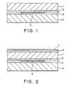
- optical cards basically have a layer construction as shown in Fig. 1.
- numeral 1 designates a transparent protective layer as a support.
- Materials for the transparent protective layer are not particularly limited so far as they exhibit high light transmission in a wavelength region of light from a light source used for recording and reproduction of information, cause neither deformation nor deterioration in steps after the formation of the optical card, and satisfy mechanical strength and optical properties requirements.
- Materials commonly used for the transparent protective layer include polycarbonate, acrylic, urethane, epoxy, polyvinyl chloride, polyolefin, and styrene/polycarbonate blend resins.
- Numeral 2 designates a pattern layer provided by photopolymer process (2P method) on the undersurface of the transparent protective layer 1.
- the interface between layers 1 and 2 disappears by use of injection or casting method.
- the patter layer is provided with grooves as tracks.
- Numeral 3 designates an optical recording material layer provided so as to cover the grooves of the pattern layer 2.
- the optical recording material layer is generally formed of an inorganic material, for example, a low-melting metal, such as tellurium, bismuth, or aluminum or an alloy thereof, or an organic dye, such as anthraquinone, naphthoquinone, triphenylmethane, carbocyanine, merocyanine, xanthene, azo, azine, thiazine, oxazine, or phthalocyanine dye.
- a low-melting metal such as tellurium, bismuth, or aluminum or an alloy thereof
- an organic dye such as anthraquinone, naphthoquinone, triphenylmethane, carbocyanine, merocyanine, xanthene, azo
- the optical recording material layer is formed of a high-reflective metal, such as aluminum, with information being previously recorded thereon.
- Numeral 4 designates a card substrate which supports an optical recording member having the above construction through an adhesive layer 5.
- the above optical card has such a structure that the optical recording material layer 3 is sandwiched between the transparent protective layer 1 on the top side of the card and the card substrate 4 on the back side of the card.
- a surface hard layer is provided on the top surface of the transparent protective layer 1 for the purpose of preventing the creation of flaws during carrying or during use of the card, thereby improving the durability of the card and the reliability of the writing and reading accuracy.
- the surface hard layer is, in many cases, formed using a radiation-curable resin.
- the polycarbonate resin is advantageously inexpensive, does not absorb water, causes neither warping nor cracking, and has excellent bending strength.
- the use of the polycarbonate resin for the transparent protective layer necessitates providing a surface hard layer from the viewpoint of increasing the scratch resistance of the card.
- the formation of a surface hard layer using a conventional radiation-curable resin having a large shrinkage on the transparent protective layer results in a fear of shrinkage during radiation curing to cause warpage or cracking by bending.
- the surface hard layer should not be formed in a thickness of not less than 15 ⁇ m.
- the hardness of the surface hard layer is influenced by the underlying transparent protective layer in a pencil hardness test, so that the pencil hardness is as low as about F to HB. Therefore, in this case, a surface hard layer having a pencil hardness of H or higher, which offers satisfactory scratch resistance, cannot be provided.
- an object of the present invention is to provide an optical recording medium which has excellent scratch resistance and causes neither warpage nor cracking by bending.
- the European Search Report cites EP-A-0,345,360 in which a substrate carrying an optical information recording layer is covered by a transparent hard layer of cured resin, optionally as a multilayer structure comprising additionally an adhesive layer and an intermediate layer.
- an optical recording medium comprising:
- the hardness of the surface hard layer is higher than that of the intermediate layer.
- an optical recording medium comprising at least a transparent protective layer and an optical recording layer laminated on top of the other, characterised in that
- an optical recording medium comprising a laminate of at least a transparent protective layer and an optical recording layer, the transparent protective layer bearing a hard layer formed of a cured resin, characterised in that
- an optical recording medium comprising a laminate of at least a transparent protective layer and an optical recording layer, the transparent protective layer bearing a hard layer formed of a cured resin, characterised in that
- an optical recording medium in accordance with the second aspect, in which all the layers constituting the hard layer, except for the innermost layer, contain at least one kind of an organic polymer type levelling agent.
- an optical recording medium in accordance with the second aspect, in which all the layers constituting the hard layer, except for the outermost layer, containing an organic polymer type levelling agent in combination with a silicone.
- an optical recording medium in accordance with the second aspect, in which a magnetic strip is provided on the transparent protective layer side.
- a sublimation or fusion type thermal transferred image and/or character information may also be provided on the card substrate.
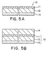
- Fig. 2 is a cross-sectional view of an optical recording medium (optical card) according to an embodiment of the first aspect of the invention.
- the optical card according to this embodiment has the following construction.
- a pattern layer 2 and an optical recording material layer 3 covering grooves of the pattern layer 2 are provided on the undersurface of the transparent protective layer 1.
- a card substrate 4 is laminated through an adhesive layer 5 so as to sandwich the optical recording material layer 3 between the card substrate and the pattern layer 2.
- An intermediate layer 6 and a surface hard layer 7 are laminated on the transparent protective layer 1.
- the polycarbonate resin (PC) used for constituting the transparent protective layer 1 preferably has good optical properties. Specifically, the use of a polycarbonate resin having a light beam transmittance of not less than 90% (780 nm, 830 nm), a refractive index of not more than 1.59 (780 nm, 830 nm), a optical retardation of not more than 100 nm (single pass), or an optical elastic axis of not more than ⁇ 5% is preferred.
- the total thickness of the transparent protective layer and the hard surface layer is preferably 380 ⁇ 20 ⁇ m. More specifically, when 2P is used for the formation of the pattern layer 2, an extruded film, for example, Panlite Film manufactured by Teijin Ltd. or Lexan Film manufactured by GE, may be used.
- the intermediate layer 6 is formed in a thickness of not less than 20 ⁇ m using a radiation-curable resin, having a shrinkage of not more than 12%, containing a functional monomer and/or a functional oligomer.
- a radiation-curable resin having a shrinkage of 12.3% on a 0.4 mm-thick PC sheet having a size of 200 mm x 200 mm and put on a desk
- the warpage of the PC sheet becomes 4.5 mm.
- a warpage of not less than 4 mm leads to a trouble in subsequent steps.
- the functional monomer examples include polyfunctional acrylates including monofunctional acrylates, (such as 2-ethylhexyl acrylate, 2-hydroxyethyl acrylate, 2-hydroxypropyl acrylate), difunctional acrylates (such as 1,3-butanediol diacrylate, 1,4-butanediol diacrylate, 1,6-hexanediol diacrylate, diethylene glycol diacrylate, neopentyl glycol diacrylate), trifunctional acrylates (such as pentaerythritol triacrylate, trimethylolpropane triacrylate), tetrafunctional acrylates (such as pentaerythritol tetraacrylate), pentafunctional acrylates (such as dipentaerythritol pentaacrylate), hexafunctional acrylates (such as dipentaerythritol hexaacrylate), and pentaor higher functional acrylates (such as dipentaeryth
- Examples of the functional oligomer include epoxy acrylate, urethane acrylate, polyester acrylate, polyether acrylate, silicone acrylate, unsaturated polyester, and polyene/thiol.
- the functional monomer and/or functional oligomer may be used in combination with N-vinylpyrrolidone as an agent for improving the adhesion to the polycarbonate and a reaction retardant, IrgacureTM 651 or 184 as an initiator (a benzoin, acetophenone, thioxanthone, peroxide or other initiator) to prepare a radiation-curable resin having a shrinkage of not more than 12%.
- a photopolymerization initiation assistant an amine, quinone or other assistant
- a heat polymerization inhibitor a filler (an inorganic or organic filler), a thixotropic agent, a plasticizer, an unreactive polymer, or a colorant may be added.
- the use of a polyfunctional acrylate is likely to increase the hardness. In this case, however, the shrinkage becomes large.
- the shrinkage should be not more than 12% in order to provide a low warpage and ensure satisfactory hardness because a surface hard layer having a thickness of not less than 20 ⁇ m is provided for avoiding the influence of the substrate.
- a shrinkage of 10% and a thickness of 25 to 30 ⁇ m are suitable in order to satisfy warpage and hardness requirements.
- N-vinylpyrrolidone as an agent for improving the adhesion to the polycarbonate and a reaction retardant and an initiator are added to a tri- to hexafunctional monomer as a functional monomer.
- an internal curing type silicone or a silicone is added as a leveling agent in an amount of 0.01 to 10 parts by weight based on 100 parts by weight of the functional monomer or functional oligomer.
- the addition of the leveling agent in an amount exceeding 10 parts by weight is unfavorable because the adhesion to the intermediate 6 is likely to be lowered.
- the leveling agent serves to reduce surface defects and, at the same time, increase the apparent hardness because the slip property is improved.
- a small amount of a functional oligomer may be added in order to ensure a certain degree of bending strength.
- a photopolymerization initiation assistant an amine, quinone or other assistant
- a heat polymerization inhibitor an amine, quinone or other assistant
- a filler an inorganic or organic filler
- a thixotropic agent a plasticizer
- an unreactive polymer or a colorant may be added.
- a thickness of more than 15 ⁇ m is unfavorable because the warpage of the optical card is likely to increase and the bending strength is lowered. More specifically, cracking occurs in a bending test. On the other hand, when the thickness is less than 2 ⁇ m, the hardness becomes unsatisfactory.
- the thickness of the surface hard layer is preferably in the range of from 2 to 15 ⁇ m, still preferably 2 to 8 ⁇ m.
- the resin used for constituting the intermediate layer may be added in an amount of not more than 30% in order to further increase the bending strength.
- An antistatic agent may be added to the intermediate layer 6 and/or the surface hard layer 7 for antistatic purposes.
- the intermediate layer 6 and the surface hard layer 7 may be formed by gravure coating, roll coating, Karla coating, spin coating, knife coating, silk screen coating, T-die coating, slide coating or slit reverse coating. In this case, coating may be carried out after dilution with a solvent to a suitable extent. It should be noted that the intermediate layer 6 may be formed by multicoat coating to have a multilayer structure.
- the pattern layer 2 provided on the undersurface of the transparent protective layer 1 may be generally formed by 2P, injection, casting, or other known methods.
- the resin used is a UV-curable resin.
- the resin used may be the same as that used in the transparent protective layer.
- the optical recording material layer 3 may be formed of a commonly used metallic optical recording material, such as a tellurium- or bismuth-based material. It may also be formed of a dye optical recording material, such as phthalocyanine- or naphthoquinone-based recording material.
- the optical recording material layer may be of ROM type as well as write-once read-many type.
- the card substrate 4 may be formed of polyvinyl chloride, polyethylene terephthalate, acrylic styrene (AS), ABS, polycarbonate or polypropylene.
- the layer construction may be of any of a three-layer type such as 0.05/0.20/0.05 mm, 0.05/0.24/0.05 mm, 0.05/0.26/0.05 mm, 0.05/0.30/0.05 mm, a two-layer type such as 0.20/0.10 mm, 0.24/0.10 mm, 0.26/0.10 mm, 0.30/0.10 mm, a single layer type such as 0.30 mm, 0.34 mm, 0.36 mm, or 0.40 mm.
- the card substrate In order to enhance the abrasion resistance of a print, it is preferred for the card substrate to have a two- or three-layer structure prepared by conducting printing on a pearlescent polyvinyl chloride and heat-sealing a transparent polyvinyl chloride to the printed pearlescent polyvinyl chloride.
- Known adhesives such as urethane, epoxy, acrylic, vinyl, and amide adhesives, may be used as an adhesive for the adhesive layer 5. Since, however, the adhesive comes into direct contact with the optical recording material layer, it preferably has high recording sensitivity and excellent temperature and moisture resistance.
- the thickness of the adhesive layer is preferably 10 to 100 ⁇ m, and gravure coating, spin coating, knife coating, silk screen coating, Mayer bar coating or T-die coating may be used to form the adhesive layer.
- the bonding may be carried out by hot pressing using a flat press or a roll press.
- a sensitizing layer may be provided between the optical recording material layer and the adhesive layer.
- the provision of the sensitizing layer is unnecessary when the recording sensitivity is satisfactory.
- the adhesive layer is in contact with the optical recording material layer. If the adhesive deteriorates the sensitivity of the optical recording material layer, a transparent protective layer may be provided for avoiding this unfavorable phenomenon.
- the sensitizing layer is provided, the transparent protective layer is provided between the sensitizing layer and the adhesive layer. However, the transparent protective layer may serve also as the sensitizing layer.
- the adhesive layer is formed of a material which does not deteriorate the optical recording material layer, there is no need to provide the transparent protective layer.
- a magnetic stripe may be provided on one side of the card substrate, which is the same as or opposite to the side where the optical recording material is provided, or both sides of the card substrate, and an IC module may be provided on one side of the card substrate which is the same as or opposite to the side where the optical recording material is provided.
- the optical recording medium comprises at least a transparent protective layer and an optical recording layer laminated on top of the other, the transparent protective layer bearing a multilayered hard layer, layers constituting the hard layer having been formed by using radiation-curable resins in such a manner that the shrinkage on curing of the radiation-curable resins successively increases from the innermost layer toward the outermost layer, the thickness of the layers constituting the hard layer being successively reduced from the innermost layer toward the outermost layer.
- a leveling agent to the outermost layer in the hard layer or to add an internal curing type leveling agent to all the layers constituting the hard layer except for the outermost layer. Further, the addition of an antistatic agent to each of the layers constituting the hard layer is preferred.
- the use of a radiation-curable resin having a low shrinkage on curing enables the warpage of the transparent protective layer to be suppressed on a small level even though the radiation-curable resin is coated in a large thickness on the transparent protective layer. Therefore, in this case, coating may be carried out in a thickness large enough to avoid the influence of the underlying transparent protective layer in a pencil hardness test. The coating in such a thickness can provide a pencil hardness of H to 2H.
- the radiation-curable resin having a low shrinkage on curing is flexible.
- the hard layer formed using such a resin has low resistance to abrasion, such as Taber abrasion (a Taber abrasion test specified in ASTM D1044) and a falling sand abrasion test (specified in JIS T8147) although the pencil hardness can be improved by increasing the coating thickness of the radiation-curable resin.
- a radiation-curable resin having a large shrinkage on curing has excellent resistance to abrasion, such as Taber abrasion, although the warpage on shrinkage is large.
- a multilayered hard layer comprising layers formed by using radiation-curable resins in such a manner that the shrinkage on curing of the radiation-curable resins successively increases from the innermost layer toward the outermost layer, the thickness of the layers being successively reduced from the innermost layer toward the outermost layer, can offer an optical recording medium which has a lowered warpage and, by virtue of synergistic effect of the layers constituting the hard layer, has excellent pencil hardness and resistance to abrasion such as Taber abrasion.
- Fig. 3 is a cross-sectional view of an embodiment of an optical card which is one form of the optical recording medium of the present invention.
- the optical card has the following construction.
- a pattern layer 2 and an optical recording layer 3 covering grooves of the pattern layer 2 are provided on the undersurface of a transparent protective layer 1.
- a card substrate 4 is laminated through an adhesive layer 5 so as to sandwich the optical recording layer 3 between the card substrate 4 and the pattern layer 2.
- a hard layer 9, having a three-layer structure, of a first layer 6a, a second layer 7, and a third layer 8 is laminated on the transparent protective layer 1.
- the resin used for constituting the transparent protective layer 1 preferably has good optical properties. Specifically, the use of a resin having a light beam transmittance of not less than 90% (780 nm, 830 nm), an optical retardation of not more than 100 nm (single pass), or an optical elastic axis of not more than ⁇ 5% is preferred.
- the total thickness of the transparent protective layer and the hard layer 9 is preferably 380 ⁇ 20 ⁇ m.
- a polycarbonate resin (PC) is particularly preferred, and it is also possible to use an acrylic resin having the above optical properties.
- an extruded polycarbonate resin film for example, Panlite Film manufactured by Teijin Ltd. or Lexan Film manufactured by GE, may be used.
- the interface between the layers 1 and 2 disappears by use of injection or casting method.
- the first layer 6a in the hard layer 9 is formed in a thickness of not less than 20 ⁇ m using a radiation-curable resin, having a low shrinkage on curing, containing a functional monomer and/or a functional oligomer on the transparent protective layer 1.
- the functional monomer examples include polyfunctional acrylates including monofunctional acrylates, (such as 2-ethylhexyl acrylate, 2-hydroxyethyl acrylate, 2-hydroxypropyl acrylate), difunctional acrylates (such as 1,3-butanediol diacrylate, 1,4-butanediol diacrylate, 1,6-hexanediol diacrylate, diethylene glycol diacrylate, neopentyl glycol diacrylate), trifunctional acrylates (such as pentaerythritol triacrylate, trimethylolpropane triacrylate), tetrafunctional acrylates (such as pentaerythritol tetraacrylate), pentafunctional acrylates (such as dipentaerythritol pentaacrylate), hexafunctional acrylates (such as dipentaerythritol hexaacrylate), and penta- or higher functional acrylates (such as dipentaery
- Examples of the functional oligomer include epoxy acrylate, urethane acrylate, polyester acrylate, polyether acrylate, silicone acrylate, unsaturated polyester, and polyene/thiol.
- the functional monomer and/or functional oligomer may be used in combination with N-vinylpyrrolidone as an agent for improving the adhesion to the polycarbonate and a reaction retardant, IrgacureTM 651 or 184 as an initiator (a benzoin, acetophenone, thioxanthone, peroxide or other initiator) to prepare a radiation-curable resin having a shrinkage on curing of not more than 12%.
- a photopolymerization initiation assistant an amine, quinone or other assistant
- a heat polymerization inhibitor e.g., a heat polymerization inhibitor
- a filler e.g., a filler, a thixotropic agent, a plasticizer, an unreactive polymer or a colorant
- a polyfunctional acrylate is likely to increase the hardness, resulting in increased shrinkage on curing.
- the shrinkage on curing should be not more than 12% in order to form the first layer 6 in a thickness of not less than 20 ⁇ m, i.e., a thickness large enough to avoid the influence of the underlying layer, and, at the same time, to provide a low warpage and to ensure satisfactory hardness.
- a thickness of 25 to 30 ⁇ m is most preferred.
- the second layer 7 is formed using a radiation-curable resin of which the hardness and the shrinkage on curing are between those of the above first layer 6a and those of the third layer 8 described below. More specifically, a functional monomer and a functional oligomer may be selected so as for the shrinkage on curing of the radiation-curable resin to be 12 to 15%. A thickness of 10 to 20 ⁇ m is most preferred for the second layer 7.
- the third layer 8 is formed, on the second layer 7, using a radiation-curable resin, having a relatively high shrinkage on curing, comprising a tri- to hexafunctional monomer as a main agent and a minor amount of a functional oligomer added to the main agent, because it should have hardness high enough to be used as a surface layer.
- a radiation-curable resin having a relatively high shrinkage on curing, comprising a tri- to hexafunctional monomer as a main agent and a minor amount of a functional oligomer added to the main agent, because it should have hardness high enough to be used as a surface layer.
- a leveling agent such as a silicone, in an amount of 0.01 to 10 parts by weight based on 100 parts by weight of the solid matter is preferred.
- the leveling agent serves to reduce surface defects and, at the same time, to increase the apparent hardness because the slip property is improved.
- the addition of the leveling agent in an amount exceeding 10 parts by weight results in deteriorated adhesion to the second layer 7, while the addition of the leveling agent in an amount of less than 0.01 part by weight offers no effect.
- a photopolymerization initiation assistant an amine, quinone or other assistant
- a heat polymerization inhibitor an amine, quinone or other assistant
- a filler an inorganic or organic filler
- a thixotropic agent a plasticizer
- an unreactive polymer or a colorant may be added.
- the proportion of the functional oligomer may be increased.
- the resin used for constituting the second layer 7 may be incorporated in an amount of 0 to 30%.
- the shrinkage on curing of the radiation-curable resin used is regulated to not less than 15%.
- the thickness of the third layer 8 is larger than 15 ⁇ m, the warpage of the optical card becomes large. Further, in this case, cracking occurs in a bending test, that is, the bending strength is unsatisfactory.
- the thickness is preferably 2 to 15 ⁇ m. However, a thickness of 2 to 5 ⁇ m is most preferred from the viewpoint of satisfying both the bending strength and hardness requirements.
- An antistatic agent may be added to the first layer 6a, the second layer 7, and the third layer 8 constituting the hard layer 9 for antistatic purposes.
- All the first layer 6a, the second layer 7, and the third layer 8 may be formed by gravure coating, roll coating, Karla coating, spin coating, knife coating, silk screen coating, T-die coating, slide coating or slit reverse coating. In this case, coating may be carried out after dilution with a solvent to a suitable extent.
- the first layer 6a and the second layer 7 may be formed by multicoat coating to have a multilayer structure.
- a leveling agent is preferably added to the first layer 6a and the second layer 7. Since, however, bleeding of the leveling agent on the surface deteriorates the adhesion, the use of an internal curing type leveling agent is preferred.
- the hard layer may have a two-, four-, or five-layer structure.
- the formation of layers for constituting the hard layer using radiation-curable resins in such a manner that the shrinkage on curing of the radiation-curable resins increases from the innermost layer toward the outermost layer enables the hardness of the cured surface to be increased while preventing the warpage of the card. Further, good bending strength can be ensured when the thickness of the layers constituting the hard layer is reduced from the innermost layer toward the outermost layer. Since the warpage of the card varies depending upon the shrinkage on curing and the thickness of the layers, the final layer construction may be determined using the shrinkage on curing and the thickness of the layers as parameters so as to minimize the warpage.
- the pattern layer 2 provided on the undersurface of the transparent protective layer 1 may be generally formed by 2P, injection, casting, or other known methods.
- the resin used is a UV-curable resin.
- the resin used may be the same as that used in the transparent protective layer 1.
- the optical recording layer 3 may be formed of a commonly used metallic optical recording material, such as a tellurium- or bismuth-based material. It may also be formed of a dye optical recording material, such as phthalocyanine- or naphthoquinone-based recording material.
- the optical recording layer 3 may be of ROM type as well as write-once read-many type.
- the card substrate 4 may be formed of polyvinyl chloride, polyethylene terephthalate, acrylic styrene (AS), ABS, polycarbonate or polypropylene.
- the layer construction may be of any of a three-layer type such as 0.05/0.20/0.05 mm, 0.05/0.24/0.05 mm, 0.05/0.26/0.05 mm, 0.05/0.30/0.05 mm, a two-layer type such as 0.20/0.10 mm, 0.24/0.10 mm, 0.26/0.10 mm, 0.30/0.10 mm, a single layer type such as 0.30 mm, 0.34 mm, 0.36 mm, or 0.40 mm.
- the card substrate In order to enhance the abrasion resistance of a print, it is preferred for the card substrate to have a two- or three-layer structure prepared by conducting printing on a pearlescent polyvinyl chloride and heat-sealing a transparent polyvinyl chloride to the printed pearlescent polyvinyl chloride.
- Known adhesives such as urethane, epoxy, acrylic, vinyl, and amide adhesives, may be used as an adhesive for the adhesive layer 5. Since, however, the adhesive comes into direct contact with the optical recording layer 3, it preferably has high recording sensitivity and excellent temperature and moisture resistance.
- the thickness of the adhesive layer is preferably 10 to 100 ⁇ m, and gravure coating, spin coating, knife coating, silk screen coating, Mayer bar coating or T-die coating may be used to form the adhesive layer.
- the bonding may be carried out by hot pressing using a flat press or a roll press.
- a sensitizing layer may be provided between the optical recording layer 3 and the adhesive layer 5.
- the provision of the sensitizing layer is unnecessary when the recording sensitivity is satisfactory.
- the adhesive layer 5 is in contact with the optical recording layer 3. If the adhesive deteriorates the sensitivity of the optical recording layer 3, a transparent protective layer may be provided for avoiding this unfavorable phenomenon.
- the sensitizing layer is provided, the transparent protective layer is provided between the sensitizing layer and the adhesive layer 5.
- the transparent protective layer may serve also as the sensitizing layer.
- the adhesive layer is formed of a material which does not deteriorate the optical recording layer 3, there is no need to provide the transparent protective layer.
- a magnetic stripe may be provided on one side of the card substrate 4, which is the same as or opposite to the side where the optical recording medium is provided, or both sides of the card substrate 4, and an IC module may be provided on one side of the card substrate 4 which is the same as or opposite to the side where the optical recording medium is provided.
- the optical recording medium comprises a laminate of at least a transparent protective layer and an optical recording layer, the transparent protective layer bearing a hard layer formed of a cured resin, the hardness of the hard layer increasing continuously from the interface of the hard layer and the transparent protective layer toward the outer surface of the hard layer.
- the cured layer may contain a leveling agent and an antistatic agent.
- an optical recording medium having the above construction may be produced by the following process.
- the fourth aspect of the invention provides a process for producing an optical recording medium comprising a laminate of at least a transparent protective layer and an optical recording layer, the transparent protective layer bearing a hard layer formed of a cured resin, wherein a plurality of curable resins different from each other or one another in shrinkage on curing are simultaneously fed in such a manner that they are put on top of the other or one another so that the shrinkage on curing of the curable resins increases from the interface of the curable resin and the transparent protective layer toward the outer surface of the resultant laminate, and the plurality of layers constituting the laminate are collectively cured to form a hard layer.
- the formation of the layers by wet-to-wet coating followed by simultaneous curing enables a plurality of hard layer to be formed in a laminate form without creating any clear interface between the layers.
- the surface hard layer thus obtained has excellent properties.
- the use of a radiation-curable resin having a low shrinkage on curing enables the warpage of the transparent protective layer to be suppressed on a small level even though the radiation-curable resin is coated in a large thickness on the transparent protective layer. Therefore, in this case, coating may be carried out in a thickness large enough to avoid the influence of the underlying transparent protective layer in a pencil hardness test. The coating in such a thickness can provide a pencil hardness of H to 2H.
- the radiation-curable resin having a low shrinkage on curing is flexible.
- the hard layer formed using such a resin has low resistance to abrasion such as Taber abrasion (a Taber abrasion test specified in ASTM D1044) and a falling sand abrasion test (specified in JIS T8147) although the pencil hardness can be improved by increasing the coating thickness of the radiation-curable resin.
- a radiation-curable resin having a large shrinkage on curing has excellent resistance to abrasion, such as Taber abrasion, although the warpage on shrinkage is large.
- the provision of a hard layer of which the hardness continuously increases from the interface of the hard layer and the transparent protective layer toward the surface of the hard layer can suppress warpage and, at the same time, provides excellent pencil hardness and resistance to abrasion such as Taber abrasion.
- the bending strength is excellent because no interface is present in the hard layer as the surface layer.
- Fig. 4 is a cross-sectional view of an embodiment of an optical card which is one form of the optical recording medium of the present invention.
- the optical card has the following construction.
- a pattern layer 2 and an optical recording layer 3 covering grooves of the pattern layer 2 are provided on the undersurface of a transparent protective layer 1.
- a card substrate 4 is laminated through an adhesive layer 5 so as to sandwich the optical recording layer 3 between the card substrate 4 and the pattern layer 2.
- a hard layer 6 apparently comprising a first layer a , a second layer b , and a third layer c is laminated on the transparent protective layer 1.
- three curable resins different from one another in shrinkage on curing are simultaneously fed in such a manner that they are put on top of one another and the resultant layers are collectively cured to form a hard layer. This causes resins to be mixed together in the area of contact with each other, eliminating the interface of the resins. Therefore, the hardness of the hard layer continuously changes from the interface of the hard layer and the transparent protective layer toward the outer surface of the hard layer.
- the resin used for constituting the transparent protective layer 1 preferably has good optical properties. Specifically, the use of a resin having a light beam transmittance of not less than 90% (780 nm, 830 nm), an optical retardation of not more than 100 nm (single pass), or an optical elastic axis of not more than ⁇ 5% is preferred.
- the total thickness of the transparent protective layer and the hard layer 6 is preferably 380 ⁇ 20 ⁇ m.
- a polycarbonate resin (PC) is particularly preferred, and it is also possible to use an acrylic resin having the above optical properties.
- an extruded polycarbonate resin film for example, Panlite Film manufactured by Teijin Ltd. or Lexan Film manufactured by GE, may be used.
- the interface between the layers 1 and 2 disappears by use of injection or casting method.
- the first layer a in the hard layer 6 is formed using a radiation-curable resin, having a low shrinkage on curing, containing a functional monomer and/or a functional oligomer.
- the functional monomer examples include polyfunctional acrylates including monofunctional acrylates, (such as 2-ethylhexyl acrylate, 2-hydroxyethyl acrylate, 2-hydroxypropyl acrylate), difunctional acrylates (such as 1,3-butanediol diacrylate, 1,4-butanediol diacrylate, 1,6-hexanediol diacrylate, diethylene glycol diacrylate, neopentyl glycol diacrylate), trifunctional acrylates (such as pentaerythritol triacrylate, trimethylolpropane triacrylate), tetrafunctional acrylates (such as pentaerythritol tetraacrylate), pentafunctional acrylates (such as dipentaerythritol pentaacrylate), hexafunctional acrylates (such as dipentaerythritol hexaacrylate), and penta-or higher functional acrylates (such as dipentaery
- Examples of the functional oligomer include epoxy acrylate, urethane acrylate, polyester acrylate, polyether acrylate, silicone acrylate, unsaturated polyester, and polyene/thiol.
- the functional monomer and/or functional oligomer may be used in combination with N-vinylpyrrolidone as an agent for improving the adhesion to the polycarbonate and a reaction retardant, IrgacureTM 651 or 184 as an initiator (a benzoin, acetophenone, thioxanthone, peroxide or other initiator) to prepare a radiation-curable resin having a shrinkage on curing of not more than 12%.
- a photopolymerization initiation assistant an amine, quinone or other assistant
- a heat polymerization inhibitor an amine, quinone or other assistant
- a filler an inorganic or organic filler
- a thixotropic agent a plasticizer
- an unreactive polymer or a colorant may be added.
- a polyfunctional acrylate is likely to increase the hardness, resulting in increased shrinkage on curing.
- the shrinkage on curing should be not more than 12% in order to form the first layer a in a thickness of not less than 20 ⁇ m, i.e., a thickness large enough to avoid the influence of the underlying layer, and, at the same time, to provide a low warpage and to ensure satisfactory hardness.
- the pencil hardness is about 2H as measured on glass.
- the apparent thickness is most preferably 25 to 30 ⁇ m.
- the second layer b is formed using a radiation-curable resin of which the hardness and the shrinkage on curing are between those of the above first layer a and those of the third layer c described below. More specifically, a functional monomer and a functional oligomer may be selected so as for the shrinkage on curing of the radiation-curable resin to be 12 to 15%.
- the pencil hardness is about 4H as measured on glass.
- the apparent thickness is preferably 10 to 20 ⁇ m.
- a leveling agent may be added to the radiation-curable resins for the first layer a and the second layer b .
- the third layer c is formed, on the second layer b , using a radiation-curable resin, having a relatively high shrinkage on curing, comprising a tri- to hexafunctional monomer as a main agent and a minor amount of a functional oligomer added to the main agent, because it should have hardness high enough to be used as a surface layer.
- a radiation-curable resin having a relatively high shrinkage on curing, comprising a tri- to hexafunctional monomer as a main agent and a minor amount of a functional oligomer added to the main agent, because it should have hardness high enough to be used as a surface layer.
- N-vinylpyrrolidone as an agent for improving the adhesion and a reaction retardant and an initiator
- a leveling agent such as a silicone
- the leveling agent serves to reduce surface defects and, at the same time, to increase the apparent hardness because the slip property is improved.
- the proportion of the functional oligomer may be increased.
- a photopolymerization initiation assistant an amine, quinone or other assistant
- a heat polymerization inhibitor an amine, quinone or other assistant
- a filler an inorganic or organic filler
- a thixotropic agent a plasticizer
- an unreactive polymer or a colorant may be added.
- the thickness is less than 2 ⁇ m, the hardness is unsatisfactory.
- the thickness is preferably 2 to 15 ⁇ m.
- a thickness of 2 to 10 ⁇ m is most preferred from the viewpoint of satisfying both the bending strength and hardness requirements.
- the resin used for constituting the second layer b may be, if necessary, added in an amount of 0 to about 30%.
- the pencil hardness is about 6 to 7H as measured on glass.
- the shrinkage on curing is regulated to not less than 15%.
- An antistatic agent may be added to the first layer a , the second layer b , and the third layer c for antistatic purposes.
- the first layer a , the second layer b , and the third layer c are simultaneously formed by slide coating on the transparent protective layer 1. Specifically, these layers are extruded through a slide head and coated so as to be put on top of one another in a wet state.
- the first layer a , the second layer b , and the third layer c formed by coating are delicately mixed together in the course of air drying or thermodrying, and the interface of layers become apparently eliminated before radiation curing. Then, a radiation is applied to conduct curing. The elimination of the interface results in improved bending strength.
- the above coating may be carried out after dilution with a solvent to a suitable extent. Further, it is also possible to use curtain coating, slot coating or the like. Specific examples of the coating method are described in Japanese Patent Publication Nos. 8977/1958 and 12390/1970, Japanese Patent Laid-Open No. 115214/1977, and Japanese Patent Publication Nos. 22192/1988 and 18143/1990.
- the hard layer may have a two-, four-, or five-layer structure.
- the formation of layers for constituting the hard layer using radiation-curable resins in such a manner that the shrinkage on curing of the radiation-curable resins increases from the interface of the hard layer and the transparent protective layer 1 toward the outer surface of the hard layer enables the hardness of the cured surface to be increased while preventing the warpage of the card. Further, good bending strength can be ensured when the thickness of the layers constituting the hard layer is reduced from the innermost layer toward the outermost layer.
- the final layer construction may be determined using the shrinkage on curing and the thickness of the layers as parameters so as to minimize the warpage.
- the hardness may be evaluated according to, besides pencil hardness, any of drop abrasion, steel wool abrasion and Taber abrasion.
- reaction-curable resins such as silicone and melamine resins.
- the pattern layer 2 provided on the undersurface of the transparent protective layer 1 may be generally formed by 2P, injection, casting, or other known methods.
- the resin used is a UV-curable resin.
- the resin used may be the same as that used in the transparent protective layer 1.
- the optical recording layer 3 may be formed of a commonly used metallic optical recording material, such as a tellurium- or bismuth-based material. It may also be formed of a dye optical recording material, such as phthalocyanine- or naphthoquinone-based recording material.
- the optical recording layer may be of ROM type as well as write-once read-many type.
- the card substrate 4 is formed of polyvinyl chloride, polyethylene terephthalate, ABS, polycarbonate, and polypropylene.
- the layer construction may be of any of a three-layer type such as 0.05/0.20/0.05 mm, 0.05/0.24/0.05 mm, 0.05/0.26/0.05 mm, 0.05/0.30/0.05 mm, a two-layer type such as 0.20/0.10 mm, 0.24/0.10 mm, 0.26/0.10 mm, 0.30/0.10 mm, a single layer type such as 0.30 mm, 0.34 mm, 0.36 mm, or 0.40 mm.
- the card substrate In order to enhance the abrasion resistance of a print, it is preferred for the card substrate to have a two- or three-layer structure prepared by conducting printing on a pearlescent polyvinyl chloride and heat-sealing a transparent polyvinyl chloride to the printed pearlescent polyvinyl chloride.
- Known adhesives such as urethane, epoxy, acrylic, vinyl, and amide adhesives, may be used as an adhesive for the adhesive layer 5. Since, however, the adhesive comes into direct contact with the optical recording layer 3, it preferably has high recording sensitivity and excellent temperature and moisture resistance.
- the thickness of the adhesive layer is preferably 10 to 100 ⁇ m, and gravure coating, spin coating, knife coating, silk screen coating, Mayer bar coating or T-die coating may be used to form the adhesive layer.
- the bonding may be carried out by hot pressing using a flat press or a roll press.
- a sensitizing layer may be provided between the optical recording layer 3 and the adhesive layer 5.
- the provision of the sensitizing layer is unnecessary when the recording sensitivity is satisfactory.
- the adhesive layer 5 is in contact with the optical recording layer 3. If the adhesive deteriorates the sensitivity of the optical recording layer 3 , a transparent protective layer may be provided for avoiding this unfavorable phenomenon.
- the sensitizing layer is provided, the transparent protective layer is provided between the sensitizing layer and the adhesive layer 5. However, the transparent protective layer may serve also as the sensitizing layer.
- the adhesive layer is formed of a material which does not deteriorate the optical recording layer 3, there is no need to provide the transparent protective layer.
- a magnetic stripe may be provided on one side of the card substrate 4, which is the same as or opposite to the side where the optical recording member is provided, or both sides of the card substrate 4, and an IC module may be provided on one side of the card substrate 4 which is the same as or opposite to the side where the optical recording member is provided.
- the optical recording medium comprises at least a transparent protective layer and an optical recording layer laminated on top of the other, the transparent protective layer bearing a multilayered hard layer, layers constituting the hard layer having been formed by using radiation-curable resins in such a manner that the shrinkage on curing of the radiation-curable resins for forming the layers successively increases from the innermost layer toward the outermost layer, all the layers, constituting the hard layer except for the innermost layer, containing at least one kinds of an organic polymer type leveling agent.
- the radiation-curable resin comprises a functional monomer and/or a functional oligomer.
- the functional monomer include polyfunctional acrylates including monofunctional acrylates, (such as 2-ethylhexyl acrylate, 2-hydroxyethyl acrylate, 2-hydroxypropyl acrylate), difunctional acrylates (such as 1,3-butanediol diacrylate, 1,4-butanediol diacrylate, 1,6-hexanediol diacrylate, diethylene glycol diacrylate, neopentyl glycol diacrylate), trifunctional acrylates (such as pentaerythritol triacrylate, trimethylolpropane triacrylate), tetrafunctional acrylates (such as pentaerythritol tetraacrylate), pentafunctional acrylates (such as dipentaerythritol pentaacrylate), hexafunctional acrylates (such as dipentaerythritol
- the organic polymer type leveling agent used in the present invention should be excellent in leveling function, as well as in adhesion.
- leveling function used herein is intended to mean that irregularities created on the coated surface is flattened with time.
- the organic polymer type leveling agent is effective also in preventing wrinkling, pinholes, foaming, dewetting, recessing, depression, cracking, raising and cratering.
- a convectional silicone oil or the like causes the silicone oil to gather on the surface of the coating solution to form a kind of a barrier layer which offers favorable effects, that is, serves to make the evaporation of the solvent homogeneous and, at the same time, to lower the surface tension. Since, however, the sole use of the silicone oil results in lowered adhesion, it is preferred to use the silicone oil in combination with the organic polymer type leveling agent.
- a preferred organic polymer type leveling agent can be dissolved in the radiation-curable resin and lower the surface tension of the radiation-curable resin and does not deteriorate the adhesion.
- preferred organic polymer type leveling agents in the present invention include polyvinyl butyral, and low-molecular weight cellulose. Such organic polymer rises the viscosity of the coating composition whereby foaming due to dynamic viscosity can effectively be prevented.
- internal curing type silicone and fluorine-modified copolymer can also be used for this purpose although these silicones has lower adhesiveness than ordinary polymers.
- Typical internal curing type silicones include silicone acrylates, and specific examples thereof include acrylsilane and methacrylsilane, acrylsilicone and methacrylsilicone, and phenylsilicone acrylate and m-phenylsilicone acrylate. More specific exmaples thereof include acryloxypropylmethyldimethoxysilane, acryloxypropyltrimethoxysilane, methacryloxypropylmethyldimethoxysilane, and methacryloxypropyltrimethoxysilane.
- the so-called “surfactant” may be used as the organic polymer type leveling agent. Since, however, this serves to lower the surface tension, solvents used are limited and, for example, aqueous coating, such as alcoholic or emulsion coating, are necessary. More specifically, organic polymer type leveling agents usable in this case include those manufactured by Miyoshi Oil & Fat Co., Ltd., Toho Chemical Industry Co., Ltd., and Nippon Oils & Fats Co., Ltd.
- polymers such as silicone-modified copolymers and fluorine-modified copolymers may be used as the organic polymer type leveling agent.
- organic polymer type leveling agent examples thereof include Chaline Series manufactured by Nissin Chemical Industry Co., Ltd.
- low-molecular weight cellulose is also effective as the organic polymer leveling agent contemplated herein.
- Talen, Flowlen, and Polyflow which are organic copolymers, manufactured by Kyoeisha Chemical Co., Ltd. are also effective.
- Two or more kinds of the organic polymer leveling agent can also be used in combination.
- An internal curing type silicone can preferably be added in addition to a low molecular cellulose.
- a suitable amount of a silicone may be added in addition to the organic polymer type leveling agent.
- the addition of these agents in an excessive amount is likely to cause surface defects, such as dewetting, if a raw film for the transparent protective layer has a defect. Therefore, in general, it is preferred to use the organic polymer type leveling agent in combination with the silicone.
- the proportions of the organic polymer type leveling agent and the silicone may be determined by taking into consideration the surface tension and the surface defect in the formation of the outer layer.
- the outermost layer in the hard layer there is no need to take the adhesion into consideration. Basically, consideration to leveling suffices for the outermost layer, and a silicone may be added for this purpose. It is also possible to add an organic polymer type leveling agent or to add the organic polymer type leveling agent in combination with the silicone. The addition of the silicone can improve the slip property, resulting in increased apparent hardness. Although some organic polymer type leveling agents too can improve the slip property, they are basically inferior to the silicone in improvement in slip property. The organic polymer type leveling agent, however, is superior to the silicone in resistance to high viscous soils such as derived from fingerprints.
- one of the silicone and the organic polymer type leveling agent or a combination of the silicone with the organic polymer type leveling agent are selected by taking into consideration the necessary slip property and resistance to soils which vary depending upon applications of the optical recording medium. Silicones modified with dimethyl polysiloxane polyether are preferred as the silicone.
- the use of a radiation-curable resin having a low shrinkage on curing enables the warpage of the transparent protective layer to be suppressed on a small level even though the radiation-curable resin is coated in a large thickness on the transparent protective layer. Therefore, in this case, coating may be carried out in a thickness large enough to avoid the influence of the underlying transparent protective layer in a pencil hardness test. The coating in such a thickness can provide a pencil hardness of H to 2H.
- the radiation-curable resin having a low shrinkage on curing is flexible.
- the hard layer formed using such a resin has low resistance to abrasion such as Taber abrasion (a Taber abrasion test specified in ASTM D1044) and a falling sand abrasion test (specified in JIS T8147) although the pencil hardness can be improved by increasing the coating thickness of the radiation-curable resin.
- a radiation-curable resin having a large shrinkage on curing has excellent resistance to abrasion, such as Taber abrasion, although the warpage on shrinkage is large.
- a multilayered hard layer comprising layers formed by using radiation-curable resins in such a manner that the shrinkage on curing of the radiation-curable resins successively increases from the innermost layer toward the outermost layer can offer an optical recording medium which has a lowered warpage and, by virtue of synergistic effect of the layers constituting the hard layer, has excellent pencil hardness and resistance to abrasion such as Taber abrasion.
- the radiation-curable resin has a molecular weight of several thousands though it is an oligomer, and since the molecular weight of the organic polymer is larger than that of the radiation-curable resin, the addition of an organic polymer type leveling agent results in the prevention of dewetting during coating. Therefore, the addition of an organic polymer type leveling agent or an organic polymer type leveling agent in combination with a silicone to at least radiation-curable resins for forming all the layers constituting the hard layer except for the outermost layer enables the radiation-curable resins to be satisfactorily coated and adhered to the underlying layer without dewetting even when a raw film for the transparent protective layer has distortion, deflection, protrusion or foreign matter.
- an organic polymer type leveling agent or a silicone or a combination of the organic polymer type leveling agent with the silicone may be optionally added to improve the slip property and the resistance to soils.
- the combination of a low molecular cellulose and a internal curing type silicone can be used in addition to the silicone.
- Fig. 3 is a cross-sectional view of an embodiment of an optical card which is one form of the optical recording medium of the present invention.
- the optical card has the following construction.
- a pattern layer 2 and an optical recording layer 3 covering grooves of the pattern layer 2 are provided on the undersurface of a transparent protective layer 1.
- a card substrate 4 is laminated through an adhesive layer 5 so as to sandwich the optical recording layer 3 between the card substrate 4 and the pattern layer 2.
- a hard layer 9, having a three-layer structure, of a first layer 6a, a second layer 7, and a third layer 8 is laminated on the transparent protective layer 1.
- the resin used for constituting the transparent protective layer 1 preferably has good optical properties. Specifically, the use of a resin having a light beam transmittance of not less than 90% (780 nm, 830 nm), an optical retardation of not more than 100 nm (single pass), or an optical elastic axis of not more than ⁇ 5% is preferred.
- the total thickness of the transparent protective layer and the hard layer 9 is preferably 380 ⁇ 20 ⁇ m.
- a polycarbonate resin (PC) is particularly preferred, and it is also possible to use an acrylic resin having the above optical properties.
- an extruded polycarbonate resin film for example, Panlite Film manufactured by Teijin Ltd. or Lexan Film manufactured by GE, may be used.
- the interface between layers 1 and 2 disappears by use of injection or casting method.
- the first layer 6a in the hard layer 9 is formed in a thickness of not less than 20 ⁇ m using a radiation-curable resin, having a low shrinkage on curing, containing a functional monomer and/or a functional oligomer and, as an additive, an organic polymer type leveling agent or a combination of an organic polymer type leveling agent with at least either an internal curing type silicone or a silicone on the transparent protective layer 1.
- a radiation-curable resin having a shrinkage on curing of 12.3% on a 0.4 mm-thick PC sheet having a size of 200 mm x 200 mm and put on a desk
- the warpage of the PC sheet becomes 4.5 mm.
- the functional monomer and/or functional oligomer may be used in combination with N-vinylpyrrolidone as an agent for improving the adhesion to the polycarbonate and a reaction retardant, IrgacureTM 651 or 184 as an initiator (a benzoin, acetophenone, thioxanthone, peroxide or other initiator), and an organic polymer type leveling agent or a combination of an organic polymer type leveling agent with at least either an internal curing type silicone or a silicone is added thereto to prepare a radiation-curable resin having a shrinkage on curing of not more than 12%.
- N-vinylpyrrolidone as an agent for improving the adhesion to the polycarbonate and a reaction retardant
- IrgacureTM 651 or 184 as an initiator (a benzoin, acetophenone, thioxanthone, peroxide or other initiator)
- a photopolymerization initiation assistant an amine, quinone or other assistant
- a heat polymerization inhibitor e.g., a heat polymerization inhibitor
- a filler e.g., a heat polymerization inhibitor
- a filler e.g., a heat polymerization inhibitor
- a filler e.g., a heat polymerization inhibitor
- a filler e.g., a heat polymerization inhibitor
- a filler an inorganic or organic filler
- a thixotropic agent e.g., a polymethyl methacrylate
- plasticizer e.g., a thixotropic agent
- an unreactive polymer or a colorant e.g., a colorant may be added.
- the use of a polyfunctional acrylate is likely to increase the hardness, resulting in increased shrinkage on curing.
- the shrinkage on curing should be not more than 12% in order to form the first layer 6
- the second layer 7 is formed using a radiation-curable resin of which the hardness and the shrinkage on curing are between those of the above first layer 6a and those of the third layer 8 described below. More specifically, a functional monomer and a functional oligomer may be selected so as for the shrinkage on curing of the radiation-curable resin to be about 12 to 15%.
- An organic polymer type leveling agent or a combination of an organic polymer type leveling agent with at least either an internal curing type silicone or a silicone is added also to the radiation-curable resin for forming the second layer 7.
- a thickness of 10 to 20 ⁇ m is most preferred for the second layer 7.
- the third layer 8 is formed, on the second layer 7, using a radiation-curable resin, having a relatively high shrinkage on curing, comprising a tri- to hexafunctional monomer as a main agent and a minor amount of a functional oligomer added to the main agent, because it should have hardness high enough to be used as a surface layer.
- a radiation-curable resin having a relatively high shrinkage on curing, comprising a tri- to hexafunctional monomer as a main agent and a minor amount of a functional oligomer added to the main agent, because it should have hardness high enough to be used as a surface layer.
- An organic polymer type leveling agent, a conventional silicone, or a combination of an organic polymer type leveling agent with a conventional silicone may be added to the radiation-curable resin for forming the outermost layer.
- the leveling agent when added in this manner, serves to improve the adhesion to the second layer 7, reduce surface defects and, at the same time, increase the apparent hardness because
- a photopolymerization initiation assistant an amine, quinone or other assistant
- a heat polymerization inhibitor a filler (an inorganic or organic filler), a thixotropic agent, a plasticizer, an unreactive polymer or a colorant
- the proportion of the functional oligomer may be increased.
- the resin used for constituting the second layer 7 may be incorporated in an amount of 0 to 30%. Further, the shrinkage on curing of the radiation-curable resin used is regulated to not less than 15%.
- the thickness of the third layer 8 is larger than 15 ⁇ m, the warpage of the optical card becomes large.
- the thickness is preferably 2 to 15 ⁇ m.
- a thickness of 2 to 5 ⁇ m is most preferred from the viewpoint of satisfying both the bending strength and hardness requirements.
- An antistatic agent may be added to the first layer 6a, the second layer 7, and the third layer 8 constituting the hard layer 9 for antistatic purposes.
- All the first layer 6a, the second layer 7, and the third layer 8 may be formed by gravure coating, roll coating, Karla coating, spin coating, knife coating, silk screen coating, T-die coating, slide coating or slit reverse coating. In this case, coating may be carried out after dilution with a solvent to a suitable extent.
- the first layer 6a and the second layer 7 7 may be formed by multicoat coating to have a multilayer structure.
- the leveling is unsatisfactory, resulting in many surface defects.
- the use of a silicone as a leveling agent is generally considered for preventing this unfavorable phenomenon.
- the addition of the conventional silicone to the first layer 6a and the second layer 7 causes the silicone to bleed on the surface of the layer, deteriorating the adhesion. Further, when a silicone is added in a small amount, the surface tension is not lowered, making it impossible for the silicone to serve as the leveling agent, although the wetting property is not deteriorated in subsequent steps.
- the hard layer may have a two-, four-, or five-layer structure.
- the formation of layers for constituting the hard layer using radiation-curable resins in such a manner that the shrinkage on curing of the radiation-curable resins increases from the innermost layer toward the outermost layer enables the hardness of the cured surface to be increased while preventing the warpage of the card. Further, good bending strength can be ensured when the thickness of the layers constituting the hard layer is reduced from the innermost layer toward the outermost layer. Since the warpage of the card varies depending upon the shrinkage on curing and the thickness of the layers, the final layer construction may be determined using the shrinkage on curing and the thickness of the layers as parameters so as to minimize the warpage.
- the pattern layer 2 provided on the undersurface of the transparent protective layer 1 may be generally formed by 2P, injection, casting, or other known methods.
- the resin used is a UV-curable resin.
- the resin used may be the same as that used in the transparent protective layer 1. In this case, the interface between the layers 1 and 2 disappears by use of injection or casting method.
- the optical recording layer 3 may be formed of a commonly used metallic optical recording material, such as a tellurium- or bismuth-based material. It may also be formed of a dye optical recording material, such as phthalocyanine- or naphthoquinone-based recording material.
- the optical recording layer may be of ROM type as well as write-once read-many type.
- the card substrate 4 may be formed of polyvinyl chloride, polyethylene terephthalate, acrylic styrene (AS), ABS, polycarbonate, ABS or polypropylene.
- the layer construction may be of any of a three-layer type such as 0.05/0.20/0.05 mm, 0.05/0.24/0.05 mm, 0.05/0.26/0.05 mm, 0.05/0.30/0.05 mm, a two-layer type such as 0.20/0.10 mm, 0.24/0.10 mm, 0.26/0.10 mm, 0.30/0.10 mm, a single layer type such as 0.30 mm, 0.34 mm, 0.36 mm, or 0.40 mm.
- the card substrate In order to enhance the abrasion resistance of a print, it is preferred for the card substrate to have a two- or three-layer structure prepared by conducting printing on a pearlescent polyvinyl chloride and a transparent polyvinyl chloride is heat-sealed to the printed pearlescent polyvinyl chloride.
- Known adhesives such as urethane, epoxy, acrylic, vinyl, and amide adhesives, may be used as an adhesive for the adhesive layer 5. Since, however, the adhesive comes into direct contact with the optical recording layer 3, it preferably has high recording sensitivity and excellent temperature and moisture resistance.
- the thickness of the adhesive layer is preferably 10 to 100 ⁇ m, and gravure coating, spin coating, knife coating, silk screen coating, Mayer bar coating or T-die coating may be used to form the adhesive layer.
- the bonding may be carried out by hot pressing using a flat press or a roll press.
- a sensitizing layer may be provided between the optical recording layer 3 and the adhesive layer 5.
- the provision of the sensitizing layer is unnecessary when the recording sensitivity is satisfactory.
- the adhesive layer 5 is in contact with the optical recording layer 3. If the adhesive deteriorates the sensitivity of the optical recording layer 3, a transparent protective layer may be provided for avoiding this unfavorable phenomenon.
- the sensitizing layer is provided, the transparent protective layer is provided between the sensitizing layer and the adhesive layer 5.
- the transparent protective layer may serve also as the sensitizing layer.
- the adhesive layer is formed of a material which does not deteriorate the optical recording layer 3, there is no need to provide the transparent protective layer.
- a magnetic stripe may be provided on one side of the card substrate 4, which is the same as or opposite to the side where the optical recording member is provided, or both sides of the card substrate 4, and an IC module may be provided on one side of the card substrate 4 which is the same as or opposite to the side where the optical recording member is provided.
- a surface hard layer is, if necessary, provided on the top surface of the transparent protective layer 1 for the purpose of preventing the creation of flaws during carrying or during use, thereby improving the durability of the card and the reliability of the writing and reading accuracy.
- the surface hard layer is, in many cases, formed using a radiation-curable resin.
- an additive such as a silicone
- an additive such as a silicone
- the surface hard layer in order to increase the apparent hardness of the surface hard layer.
- the magnetic stripe cannot be successfully adhered due to lowered adhesion.
- the proportion of a polyfunctional monomer capable of providing a high surface hardness is increased without adding any additive such as a silicone, the adhesion of the magnetic stripe to the surface of the hard layer is not always good.
- the magnetic stripe since a magnetic stripe is formed on the card surface, the magnetic stripe is protruded on the card surface, deteriorating the appearance of the card.
- the thickness of the surface hard layer on the magnetic stripe should be 10 ⁇ m at the largest in consideration of the output of magnetism.
- the thickness 10 ⁇ m provide no satisfactory surface hardness in the optical card.
- the present invention has been made under the above circumstances and provides an optical card provided with a magnetic stripe, which has excellent scratch resistance, causes neither warpage nor cracking by bending, and has excellent smoothness.
- the optical card of the present invention comprises: a card substrate; and, laminated on the card substrate, an optical recording member comprising a laminate of at least a transparent protective layer and an optical recording layer, a magnetic stripe being provided on the transparent protective layer side.
- a multilayered surface hard layer may be provided on the transparent protective layer formed of a radiation-cured resin, and in this case, the magnetic stripe may be provided on the surface hard layer.
- a magnetic stripe may be provided on a layer other than the outermost layer in the surface hard layer or alternatively on the transparent protective layer.
- the outermost layer in the surface hard layer and the magnetic stripe constitute an identical face, that is, the surface of the outermost layer in the surface hard layer and the surface of the area where the magnetic stripe is present constitute an identical surface and no difference in level exist in the boundary between the surface hard layer and the surface of the area where the magnetic stripe is present.
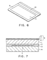
- the magnetic stripe may be any one commonly used in the conventional magnetic cards.
- a magnetic stripe 10 generally comprises a release layer 11, a magnetic layer 12, and an adhesive layer 13 provided in that order.
- a typical method for forming the magnetic stripe is as follows. As shown in Fig. 5B, after the release layer 11, the magnetic layer 12, and the adhesive layer 13 are formed on a substrate 14, the resultant laminate is slit into a predetermined width. The adhesive layer 12 of slit laminate is abutted against and heat-sealed to an adherend, and the substrate 14 is then peeled off.
- the substrate 14 is not particularly limited and may be any substrate commonly used in the conventional transfer sheet.
- Preferred specific examples of the substrate include films having high heat resistance, such as films of a polyester resin, a polyamide resin, a polyimide resin, and a polycarbonate.
- the thickness of the substrate is preferably 1 to 300 ⁇ m.
- the release layer 11 is formed of a release agent, such as a wax, a silicone wax, a silicone resin, a fluororesin, an acrylic resin.
- the release layer 11 may be formed by coating an ink of the above resin and necessary additives dissolved or dispersed in a suitable solvent onto the substrate 10 by known coating means and then drying the coating.
- the thickness of the release layer 11 is preferably 0.5 to 5 ⁇ m.
- Examples of magnetic materials for constituting the magnetic layer 12 include magnetic fine particles of ⁇ -Fe 2 O 3 , Co-coated ⁇ -Fe 2 O 3 , Fe 3 O 4 , Fe, Fe-Cr, Fe-Co, Co-Cr, Co-Ni, Ba ferrite and Sr ferrite.
- the magnetic layer 12 may be formed by coating a dispersion of the magnetic fine particles in a suitable resin or an ink vehicle by a known coating method such as gravure, roll, or knife edge coating.
- the resin or ink vehicle in which the magnetic fine particles are dispersed examples include butyral resin, vinyl chloride/vinyl acetate copolymer resin, urethane resin, polyester resin, cellulose resin, acrylic resin, styrene/malic acid copolymer resin. If necessary, rubbery resin, such as nitrile resin or urethane elastomer may be added thereto. Further, if necessary, a surfactant, a silane coupling agent, a plasticizer, a wax, a silicone oil, a pigment, such as carbon, may be added to the dispersion of magnetic fine particles in a resin or an ink vehicle.
- the thickness of the magnetic layer 12 formed by using the magnetic material, the resin or the ink vehicle is 1 to 100 ⁇ m, preferably 5 to 20 ⁇ m.
- the magnetic layer 12 may be formed by vacuum deposition, sputtering, plating or other method using a metal or an alloy, such as Fe, Fe-Cr, Fe-Co, or Co-Cr or an oxide of the above metal or alloy.
- the thickness is 0.01 ⁇ m (100 ⁇ ) to 1 ⁇ m, preferably 0.05 to 0.02 ⁇ m (500 to 2000 ⁇ ).
- the adhesive layer 13 may be formed of any conventional adhesive such as an acrylic resin, a vinyl resin, a polyester resin, a urethane resin, an amide resin, an epoxy resin, a rubbery resin, or an ionomer resin.
- the thickness of the adhesive layer 13 is 0.1 to 5 ⁇ m, preferably 1 to 10 ⁇ m.
- the radiation-curable resin for forming each layer constituting the surface hard layer comprises a functional monomer and/or a functional oligomer.
- the functional monomer include polyfunctional acrylates including monofunctional acrylates, (such as 2-ethylhexyl acrylate, 2-hydroxyethyl acrylate, 2-hydroxypropyl acrylate), difunctional acrylates (such as 1,3-butanediol diacrylate, 1,4-butanediol diacrylate, 1,6-hexanediol diacrylate, diethylene glycol diacrylate, neopentyl glycol diacrylate), trifunctional acrylates (such as pentaerythritol triacrylate, trimethylolpropane triacrylate), tetrafunctional acrylates (such as pentaerythritol tetraacrylate), pentafunctional acrylates (such as dipentaerythritol pentaacrylate), hexafunctional acrylates (such
- At least an organic polymer type leveling agent is added to all the layers constituting the surface hard layer except for the outermost layer.
- a leveling agent is indispensable in order to minimize surface defects, the addition of a suitable amount of a conventional silicone results in remarkably deteriorated adhesion of each layer in the surface hard layer.
- the organic polymer type leveling agent is as described above, and it is very important for the selected organic polymer type leveling agent to be soluble in the radiation-curable resin, to lower the surface tension of the radiation-curable resin, and not to lower the adhesion.
- a so-called "surfactant" may be used as the organic polymer type leveling agent. Since, however, this serves to lower the surface tension, solvents used are limited and, for example, aqueous coating, such as alcoholic or emulsion coating, are necessary. More specifically, organic polymer type leveling agents usable in this case include those manufactured by Miyoshi Oil & Fat Co., Ltd., Toho Chemical Industry Co., Ltd., and Nippon Oils & Fats Co., Ltd.
- silicone-modified copolymers and fluorine-modified copolymers may be used as the organic polymer type leveling agent.
- specific examples thereof include Chaline Series manufactured by Nissin Chemical Industry Co., Ltd.
- low-molecular weight cellulose and the like are also effective as the organic polymer leveling agent contemplated herein.
- Talen, Flowlen, and Polyflow which are organic copolymers, manufactured by Kyoeisha Chemical Co., Ltd. are also effective.
- a suitable amount of a silicone may be added.
- these agents in an excessive amount is likely to cause surface defects, such as dewetting, in the formation of a layer overlying the layer, to which the silicone has been added, or deteriorated adhesion to a magnetic stripe if a raw film for the transparent protective layer has a defect.
- the organic polymer type leveling agent in combination with at least either the internal curing type leveling agent or the silicone.
- the proportions of the organic polymer type leveling agent and silicone may be determined by taking into consideration the surface tension, the surface defect in the formation of the outer layer, and the adhesion to the magnetic stripe.
- the outermost layer in the surface hard layer there is no need to take the adhesion of the outer layer and the magnetic stripe into consideration. Basically, consideration to leveling suffices for the outermost layer, and a silicone may be added for this purpose. It is also possible to add an organic polymer type leveling agent or to add the organic polymer type leveling agent in combination with the silicone. The addition of the silicone can improve the slip property, resulting in increased apparent hardness. Although some organic polymer type leveling agents too can improve the slip property, they are basically inferior to the silicone in improvement in slip property. The organic polymer type leveling agent, however, is superior to the silicone in resistance to high viscous soils such as derived from fingerprints. Therefore, one of the silicone and the organic polymer type leveling agent or a combination of the silicone with the organic polymer type leveling agent are selected by taking into consideration the necessary slip property and resistance to soils which vary depending upon applications of the optical recording medium.
- the thickness of the surface hard layer provided on the magnetic stripe greatly has an effect on the output of magnetism.
- the selection of the material per se for constituting the magnetic layer 12 is important, the thickness of the surface of the surface hard layer on the magnetic stripe is preferably not more than 10 ⁇ m.
- the layer construction of the surface hard layer may be determined by taking into consideration the output of magnetism, surface hardness, and bending strength.
- the use of a radiation-curable resin having a low shrinkage on curing enables the warpage of the transparent protective layer to be suppressed on a small level even though the radiation-curable resin is coated in a large thickness on the transparent protective layer. Therefore, in this case, coating may be carried out in a thickness large enough to avoid the influence of the underlying transparent protective layer in a pencil hardness test. The coating in such a thickness can provide a pencil hardness of H to 2H.
- the radiation-curable resin having a low shrinkage on curing is flexible.
- the hard layer formed using such a resin has low resistance to abrasion such as Taber abrasion (a Taber abrasion test specified in ASTM D1044) and a falling sand abrasion test (specified in JIS T8147) although the pencil hardness can be improved by increasing the coating thickness of the radiation-curable resin.
- a radiation-curable resin having a large shrinkage on curing has excellent resistance to abrasion, such as Taber abrasion, although the warpage on shrinkage is large.
- a multilayered hard layer comprising layers formed by using radiation-curable resins in such a manner that the shrinkage on curing of the radiation-curable resins successively increases from the innermost layer toward the outermost layer can offer an optical card which has a lowered warpage and, by virtue of synergistic effect of the layers constituting the hard layer, has excellent pencil hardness and resistance to abrasion such as Taber abrasion.
- the radiation-curable resin has a molecular weight of about several thousands though it is an oligomer, and since the molecular weight of the organic polymer is larger than that of the radiation-curable resin, the addition of an organic polymer type leveling agent results in the prevention of dewetting during coating. Therefore, the addition of an organic polymer type leveling agent or a combination of an organic polymer type leveling agent with a silicone to at least radiation-curable resins for forming all the layers constituting the hard layer except for the outermost layer enables the radiation-curable resins to be satisfactorily coated and adhered to the underlying layer without dewetting even when a raw film for the transparent protective layer has distortion, deflection, protrusion or foreign matter.
- an organic polymer type leveling agent or a silicone or a combination of the organic polymer type leveling agent with the silicone may be optionally added to improve the slip property and the resistance to soils.
- the adhesion in the formation of an outer layer is taken into consideration, making it possible to provide a magnetic stripe on these layers.
- the selection of a suitable method for forming the outermost layer enables the outermost layer and the magnetic stripe to be provided so as to constitute an identical face or alternatively the magnetic stripe to be embedded in the surface hard layer.
- the adoption of such a layer construction can provide an optical card which has a magnetic stripe on the transparent protective layer side and possesses excellent surface hardness and bending strength and good surface smoothness and appearance.
- Fig. 6 is a perspective view of an embodiment of the optical card according to the present invention
- Fig. 7 a cross-sectional view of a portion including an optical recording layer.
- the optical card has the following construction.
- a pattern layer 2 and an optical recording layer 3 covering grooves of the pattern layer 2 are provided on the undersurface of a transparent protective layer 1.
- a card substrate 4 is laminated through an adhesive layer 5 so as to sandwich the optical recording layer 3 between the card substrate 4 and the pattern layer 2.
- a surface hard layer 9, having a three-layer structure, of a first layer 6, a second layer 7, and a third layer 8 is laminated on the transparent protective layer 1.
- the magnetic stripe 10 is provided in a predetermined position which does not overlap with the optical recording layer 3 in a planar relationship.
- Figs. 8 to 15 there are many embodiments on the form of provision of the magnetic stripe in the surface hard layer 9 or the transparent protective layer 1.
- the coercive force may be determined from the relationship with the magnetism R/W, and the magnetic stripe may be provided in such a form as will be compatible with the coercive force.
- the resin used for constituting the transparent protective layer 1 preferably has good optical properties. Specifically, the use of a resin having a light beam transmittance of not less than 90% (780 nm, 830 nm), an optical retardation of not more than 100 nm (single pass), or an optical elastic axis of not more than ⁇ 5% is preferred.
- the total thickness of the transparent protective layer and the hard layer 9 is preferably 380 ⁇ 20 ⁇ m.
- a polycarbonate resin (PC) is particularly preferred, and it is also possible to use an acrylic resin having the above optical properties.
- an extruded polycarbonate resin film for example, Panlite Film manufactured by Teijin Ltd. or Lexan Film manufactured by GE, may be used.
- the interface between the layers 1 and 2 disappears by use of injection or casting method.
- the pattern layer 2 provided on the undersurface of the transparent protective layer 1 may be generally formed by 2P, injection, casting, or other known methods.
- the resin used is a UV-curable resin.
- the resin used may be the same as that used in the transparent protective layer 1.
- the optical recording layer 3 may be formed of a commonly used metallic optical recording material, such as a tellurium- or bismuth-based material. It may also be formed of a dye optical recording material, such as phthalocyanine- or naphthoquinone-based recording material.
- the optical recording layer may be of ROM type as well as write-once read-many type.
- the card substrate 4 may be formed of polyvinyl chloride, polyethylene terephthalate, acrylic styrene (AS), polycarbonate, ABS or polypropylene.
- the layer construction may be of any of a three-layer type such as 0.05/0.20/0.05 mm, 0.05/0.24/0.05 mm, 0.05/0.26/0.05 mm, 0.05/0.30/0.05 mm, a two-layer type such as 0.20/0.10 mm, 0.24/0.10 mm, 0.26/0.10 mm, 0.30/0.10 mm, a single layer type such as 0.30 mm, 0.34 mm, 0.36 mm, or 0.40 mm.
- the card substrate In order to enhance the abrasion resistance of a print, it is preferred for the card substrate to have a two- or three-layer structure prepared by conducting printing on a pearlescent polyvinyl chloride and a transparent polyvinyl chloride is heat-sealed to the printed pearlescent polyvinyl chloride.
- Known adhesives such as urethane, epoxy, acrylic, vinyl, and amide adhesives, may be used as an adhesive for the adhesive layer 5. Since, however, the adhesive comes into direct contact with the optical recording layer 3, it preferably has high recording sensitivity and excellent temperature and moisture resistance.
- the thickness of the adhesive layer is preferably 10 to 100 ⁇ m, and gravure coating, spin coating, knife coating, silk screen coating, Mayer bar coating or T-die coating may be used to form the adhesive layer.
- the bonding may be carried out by hot pressing using a flat press or a roll press.
- a sensitizing layer may be provided between the optical recording layer 3 and the adhesive layer 5.
- the provision of the sensitizing layer is unnecessary when the recording sensitivity is satisfactory.
- the adhesive layer 5 is in contact with the optical recording layer 3. If the adhesive deteriorates the sensitivity of the optical recording layer 3, a transparent protective layer may be provided for avoiding this unfavorable phenomenon.
- the sensitizing layer is provided, the transparent protective layer is provided between the sensitizing layer and the adhesive layer 5.
- the transparent protective layer may serve also as the sensitizing layer.
- the adhesive layer is formed of a material which does not deteriorate the optical recording layer 3, there is no need to provide the transparent protective layer.
- the first layer 6 in the hard layer 9 is formed in a thickness of not less than 20 ⁇ m using a radiation-curable resin, having a low shrinkage on curing, containing a functional monomer and/or a functional oligomer and, as an additive, at least one kind of an organic polymer type leveling agent or a combination of an organic polymer type leveling agent with a silicone on the transparent protective layer 1.
- a radiation-curable resin having a shrinkage on curing of 12.3% on a 0.4 mm-thick PC sheet having a size of 200 mm x 200 mm and put on a desk
- the warpage of the PC sheet becomes 4.5 mm.
- the functional monomer and/or functional oligomer may be used in combination with N-vinylpyrrolidone as an agent for improving the adhesion to the polycarbonate and a reaction retardant, IrgacureTM 651 or 184 as an initiator (a benzoin, acetophenone, thioxanthone, peroxide or other initiator), and an organic polymer type leveling agent or a combination of an organic polymer type leveling agent with at least either an internal curing type silicone or a silicone is added thereto to prepare a radiation-curable resin having a shrinkage on curing of not more than 12%.
- N-vinylpyrrolidone as an agent for improving the adhesion to the polycarbonate and a reaction retardant
- IrgacureTM 651 or 184 as an initiator (a benzoin, acetophenone, thioxanthone, peroxide or other initiator)
- a photopolymerization initiation assistant an amine, quinone or other assistant
- a heat polymerization inhibitor an amine, quinone or other assistant
- a filler an inorganic or organic filler
- a thixotropic agent a plasticizer
- an unreactive polymer or a colorant may be added.
- the shrinkage on curing should be not more than 12% in order to form the first layer 6 in a thickness of not less than 20 ⁇ m, i.e., a thickness large enough to avoid the influence of the underlying layer, and, at the same time, to provide a low warpage and to ensure satisfactory hardness.
- a thickness of 20 to 30 ⁇ m is most preferred. When increasing the shrinkage on curing is contemplated, the thickness may be about 15 ⁇ m.
- the second layer 7 is formed using a radiation-curable resin of which the hardness and the shrinkage on curing are between those of the above first layer 6 and those of the third layer 8 described below. More specifically, a functional monomer and a functional oligomer may be selected so as for the shrinkage on curing of the radiation-curable resin to be 12 to 15%.
- An organic polymer type leveling agent or a combination of an organic polymer type leveling agent with at least either an internal curing type silicone or a silicone is added also to the radiation-curable resin for forming the second layer 7. A thickness of 1 to 10 ⁇ m is most preferred for the second layer 7.
- the third layer 8 is formed, on the second layer 7, using a radiation-curable resin, having a relatively high shrinkage on curing, comprising a tri- to hexafunctional monomer as a main agent and a minor amount of a functional oligomer added to the main agent, because it should have hardness high enough to be used as a surface layer.
- a radiation-curable resin having a relatively high shrinkage on curing, comprising a tri- to hexafunctional monomer as a main agent and a minor amount of a functional oligomer added to the main agent, because it should have hardness high enough to be used as a surface layer.
- An organic polymer type leveling agent, a conventional silicone, or a combination of an organic polymer type leveling agent with a conventional silicone may be added to the radiation-curable resin for forming the outermost layer.
- the leveling agent when added in such a manner, serves to improve the adhesion to the second layer 7, reduce surface defects and, at the same time, increase the apparent hard
- a photopolymerization initiation assistant an amine, quinone or other assistant
- a heat polymerization inhibitor an amine, quinone or other assistant
- a filler an inorganic or organic filler
- a thixotropic agent a plasticizer
- an unreactive polymer a colorant and the like
- the proportion of the functional oligomer may be increased.
- the resin used for constituting the second layer 7 may be incorporated in an amount of 0 to 30%. Further, the shrinkage on curing of the radiation-curable resin used is regulated to not less than 15%.
- the thickness of the third layer 8 is larger than 15 ⁇ m, the warpage of the optical card becomes large.
- the thickness is preferably 2 to 15 ⁇ m.
- a thickness of 2 to 5 ⁇ m is most preferred from the viewpoint of satisfying both the bending strength and hardness requirements.
- An antistatic agent may be added to the first layer 6, the second layer 7, and the third layer 8 for antistatic purposes.
- the magnetic stripe 10 When the magnetic stripe is provided on the transparent protective layer 1 or a layer other than the outermost layer in the surface hard layer 9, the magnetic stripe 10 is protruded from the surface of the layer. Therefore, the method for forming a layer(s) to be provided thereon is determined by a contemplated final laminate form.
- a 2P method using a specular PET or a slit reverse coating method wherein the resin is passed through a gap and enables an identical face to be formed is useful independently of irregularities on the underlying layer.
- all the first layer 6, the second layer 7, and the third layer 8 may be formed by gravure coating, roll coating, Karla coating, spin coating, knife coating, silk screen coating, T-die coating or slide coating. In this case, coating may be carried out after dilution with a solvent to a suitable extent. It should be noted that the first layer 6 and the second layer 7 may be formed by multicoat coating to have a multilayer structure.
- the addition of an organic polymer type leveling agent or a conventional silicone or the addition of an organic polymer type leveling agent with a conventional silicone is preferred in order to avoid the occurrence of surface defects or to improve the slip property of the surface of the layer.
- the hard layer may have a two-, four-, or five-layer structure.
- the formation of layers for constituting the hard layer using radiation-curable resins in such a manner that the shrinkage on curing of the radiation-curable resins increases from the innermost layer toward the outermost layer enables the hardness of the cured surface to be increased while preventing the warpage of the card. Further, good bending strength can be ensured when the thickness of the layers constituting the hard layer is reduced from the innermost layer toward the outermost layer.
- the warpage of the card varies depending upon the shrinkage on curing and the thickness of the layers, and the relationship between the layer construction and the thickness of the magnetic stripe 10 should be taken into consideration. Therefore, the final layer construction may be determined using the shrinkage on curing, the thickness of the layers, and the thickness of the magnetic stripe as parameters so as to minimize the warpage.
- a magnetic stripe 10 may be provided on the back side of the card substrate 4, and an IC chip may be provided on the same side as the optical recording face or on the opposite side of the optical recording face. It is also possible to provide at least one magnetic stripe 10 on the optical recording face and at least one magnetic stripe 10 on the back side of the card substrate 4.
- the maximum number of magnetic stripes 10, which can be provided in order to cope with conventional ATM, is four. In this case, different information may be recorded for each magnetic stripe.
- Figs. 16 to 18 two magnetic stripes 10 are provided on the optical recording face; in Fig. 17, one magnetic stripe 10 and one IC chip 15 are provided; and in Fig. 18, two magnetic stripes 10 and one IC chip 15 are provided.
- a 0.4 mm-thick extruded polycarbonate having a size of 200 mm x 200 mm was provided as a transparent protective layer, and a radiation-curable resin having the following composition was coated on one side of the transparent protective layer by means of a Mayer bar to a thickness of 30 ⁇ m, and the coating was then irradiated with ultraviolet (UV) light through a UV lamp (a microwave system, manufactured by Fusion) to cure the coating, thereby forming an intermediate layer.
- UV ultraviolet
- the shrinkage on UV curing of the radiation-curable resin was 9.6%, and the warpage was 2.5 mm at the time when the intermediate layer was formed on the transparent protective layer.
- Urethane acrylate oligomer (GohselacTM UV7500B, manufactured by Nippon Synthetic Chemical Industry Co., Ltd.) 100 parts Hexamethylene diacrylate (KayaradTM HDDA, manufactured by Nippon Kayaku Co., Ltd.) 3 parts Pentaerythritol triacrylate (AronixTM M-305, manufactured by Toa Gosei Chemical Industry Co., Ltd.) 3 parts Dipentaerythritol hexaacrylate (KayaradTM DPHA, manufactured by Nippon Kayaku Co., Ltd.) 3 parts N-Vinylpyrrolidone (AronixTM M-150, manufactured by Toa Gosei Chemical Industry Co., Ltd.) 50 parts 1-Hydroxycyclohexyl phenyl ketone (IrgacureTM 184, manufactured by Ciba-Geigy) 10 parts
- a composition prepared by dispersing 0.5 part by weight of a reactive silicone (X-22-5002, manufactured by Shin-Etsu Silicone Co., Ltd.) in 100 parts by weight of a radiation-curable resin (UV-3700, manufactured by Toa Gosei Chemical Industry Co., Ltd.) was coated on the intermediate layer by means of a Mayer bar to a thickness of 5 ⁇ m, and the coating was irradiated with ultraviolet (UV) light through a UV lamp (a microwave system, manufactured by Fusion) to cure the coating, thereby forming a surface hard layer.
- UV ultraviolet
- the Taber abrasion was 9.8% in terms of the haze as measured under conditions of CS-10, 1 kg load and 100 revolutions, and the pencil hardness (according to JIS K-5400) was H.
- a guide track pattern layer was formed by 2P method on the other side of the transparent protective layer remote from the intermediate layer and the surface hard layer. TeOx was sputtered thereon to form an optical recording material layer.
- silk offset printing was carried out on both sides of a 0.20 mm-thick core sheet of pearlescent polyvinyl chloride. This core sheet was then sandwiched between two 0.05 mm-thick overlay sheets, and heat fusing was carried out to prepare a card substrate having a three-layer structure. A magnetic tape of 650 oersted was previously formed on one side of the overlay sheet.
- the card substrate was bonded to the transparent protective layer with the aid of an adhesive (TU-4210, manufactured by Toray Industries, Inc.). After curing of the adhesive, a card (85.5 x 54 mm) was punched from the laminate, thereby preparing an optical card.
- optical card thus obtained was used to write and read data of 100 tracks by optical card R/W (3B3H-DJ-01, manufactured by Omron Corp.). As a result, the error rate was satisfactorily low and not more than 1 x 10 -4 . Further, the optical card had no problem associated with any of the bending strength, adhesion, transmission, and warpage and had good storage stability under service temperature and humidity conditions and thus was satisfactory for practical use as an optical card.
- Example 2 The same extruded polycarbonate as used in Example 1 was provided as a transparent protective layer, and a radiation-curable resin having the following composition was coated on one side of the transparent protective layer by means of a Mayer bar to a thickness of 20 ⁇ m, and the coating was then irradiated with ultraviolet (UV) light through a UV lamp (a microwave system, manufactured by Fusion) to cure the coating, thereby forming an intermediate layer.
- UV ultraviolet
- UV lamp a microwave system, manufactured by Fusion
- Urethane acrylate oligomer (GohselacTM UV7500B, manufactured by Nippon Synthetic Chemical Industry Co., Ltd.) 100 parts Pentaerythritol triacrylate (AronixTM M-305, manufactured by Toa Gosei Chemical Industry Co., Ltd) 10 parts Pentaerythritol tetraacrylate (AronixTM M-450, manufactured by Toa Gosei Chemical Industry Co., Ltd.) 10 parts Dipentaerythritol hexaacrylate (KayaradTM DPHA, manufactured by Nippon Kayaku Co., Ltd.) 3 parts N-Vinylpyrrolidone (AronixTM M-150, manufactured by Toa Gosei Chemical Industry Co., Ltd.) 50 parts 1-Hydroxycyclohexyl phenyl ketone (IrgacureTM 184, manufactured by Ciba-Geigy) 10 parts Reactive silicone (X-22-5002, manufactured by
- a radiation-curable resin having the following composition was coated on the intermediate layer by means of a Mayer bar to a thickness of 5 ⁇ m, and the coating was irradiated with ultraviolet (UV) light through a UV lamp (a microwave system, manufactured by Fusion) to cure the coating, thereby forming a surface hard layer.
- UV ultraviolet
- the Taber abrasion was 9.0% in terms of the haze as measured under conditions of CS-10, 1 kg load and 100 revolutions, and the pencil hardness was H.
- Example 1 Thereafter, the procedure of Example 1 was repeated to form a pattern layer and an optical recording material layer, and the laminate was laminated onto a card substrate, and a card was punched from the laminate, thereby preparing an optical card.
- the optical card thus obtained was used to write and read data of 100 tracks by optical card R/W (3B3H-DJ-01, manufactured by Omron Corp.). As a result, the error rate was satisfactorily low and not more than 1 x 10 -4 . Further, the optical card had no problem associated with any of the bending strength, adhesion, transmission, and warpage and good storage stability under service temperature and humidity conditions and thus was satisfactory for practical use as an optical card.
- a 0.4 mm-thick extruded polycarbonate having a size of 200 mm x 200 mm was provided as a transparent protective layer, and a radiation-curable resin having the following composition was coated on one side of the transparent protective layer by means of a Mayer bar to a thickness of 10 ⁇ m, and the coating was then irradiated with ultraviolet (UV) light through a UV lamp (a microwave system, manufactured by Fusion) to cure the coating, thereby forming a surface hard layer.
- UV ultraviolet
- the shrinkage on UV curing of the radiation-curable resin was 13.5%.
- Comparative Example A-1 The procedure of Comparative Example A-1 was repeated, except that the thickness of the surface hard layer was 25 ⁇ m. As a result, the Taber abrasion was 9.5% in terms of haze, and the pencil hardness was H. However, the warpage at this point was 4.8 mm, and a crack occurred in a bending test. Thus, when a radiation-curable resin having a large shrinkage was used, an increase in thickness resulted in increased warpage, deteriorating the bending strength.
- a polycarbonate resin is used as a transparent protective layer
- an intermediate layer having a thickness of not less than 20 ⁇ m, formed of a radiation-cured resin having a shrinkage of not more than 12% is provided on the transparent protective layer
- a surface hard layer is provided on the intermediate layer.
- a 0.4 mm-thick extruded polycarbonate having a size of 200 mm x 200 mm was provided as a transparent protective layer 1, and a radiation-curable resin having the following composition was coated on one side of the transparent protective layer by means of a Mayer bar to a thickness of 20 ⁇ m, and the coating was then irradiated with ultraviolet (UV) light through a UV lamp (a microwave system, manufactured by Fusion) to cure the coating, thereby forming a first layer 6.
- UV ultraviolet
- the shrinkage on UV curing of the radiation-curable resin was 9.6%, and the warpage was 2.5 mm at the time when the first layer 6 was formed on the transparent protective layer 1.
- Urethane acrylate oligomer (GohselacTM UV7500B, manufactured by Nippon Synthetic Chemical Industry Co., Ltd.) 100 parts Hexamethylene diacrylate (KayaradTM HDDA, manufactured by Nippon Kayaku Co., Ltd.) 3 parts Pentaerythritol triacrylate (AronixTM M-305, manufactured by Toa Gosei Chemical Industry Co., Ltd.) 3 parts Dipentaerythritol hexaacrylate (KayaradTM DPHA, manufactured by Nippon Kayaku Co., Ltd.) 3 parts N-Vinylpyrrolidone (AronixTM M-150, manufactured by Toa Gosei Chemical Industry Co., Ltd.) 50 parts 1-Hydroxycyclohexyl phenyl ketone (IrgacureTM 184, manufactured by Ciba-Geigy) 10 parts
- a radiation-curable resin having the following composition was coated on the first layer 6 by means of a Mayer bar to a thickness of 10 ⁇ m, and the coating was irradiated with ultraviolet (UV) light through a UV lamp (a microwave system, manufactured by Fusion) to cure the coating, thereby forming a second layer 7.
- UV ultraviolet
- the shrinkage on UV curing of the radiation-curable resin was 13.0%, and the warpage was 3.0 mm at the time when the second layer 7 was formed.
- Urethane acrylate oligomer (GohselacTM UV7500B, manufactured by Nippon Synthetic Chemical Industry Co., Ltd.) 80 parts Pentaerythritol triacrylate (AronixTM M-305, manufactured by Toa Gosei Chemical Industry Co., Ltd.) 10 parts Pentaerythritol tetraacrylate (AronixTM M-450, manufactured by Toa Gosei Chemical Industry Co., Ltd.) 10 parts Dipentaerythritol hexaacrylate (KayaradTM DPHA, manufactured by Nippon Kayaku Co., Ltd.) 3 parts N-Vinylpyrrolidone (AronixTM M-150, manufactured by Toa Gosei Chemical Industry Co,, Ltd.) 50 parts 1-Hydroxycyclohexyl phenyl ketone (IrgacureTM 184, manufactured by Ciba-Geigy) 10 parts
- UV ultraviolet
- the shrinkage on curing of the radiation-curable resin was 14.5%.
- the Taber abrasion was 9.8% in terms of the haze as measured under conditions of CS-10, 1 kg load and 100 revolutions, and the pencil hardness was H.
- a guide track pattern layer 2 was formed by 2P on the other side of the transparent protective layer 1 remote from the hard layer 9 formed of the first layer 6, the second layer 7, and the third layer 8. TeOx was sputtered thereon to form an optical recording layer 3.
- silk offset printing was carried out on both sides of a 0.20 mm-thick core sheet of pearlescent polyvinyl chloride. This core sheet was then sandwiched between two 0.05 mm-thick overlay sheets, and heat fusing was carried out to prepare a card substrate 4 having a three-layer structure. A magnetic tape of 650 oersted was previously formed on one side of the overlay sheet.
- the card substrate 4 was bonded to the transparent protective layer 1 with the aid of an adhesive (TU-4210, manufactured by Toray Industries, Inc.). After curing of the adhesive, a card (85.5 x 54 mm) was punched from the laminate, thereby preparing an optical card.
- an adhesive TU-4210, manufactured by Toray Industries, Inc.
- optical card thus obtained was used to write and read data of 100 tracks by optical card R/W (3B3H-DJ-01, manufactured by Omron Corp.). As a result, the error rate was satisfactorily low and not more than 1 x 10 -4 . Further, the optical card had no problem associated with any of the bending strength, adhesion, transmission, and warpage and good storage stability under service temperature and humidity conditions and thus was satisfactory for practical use as an optical card.
- Example 1 The procedure of Example 1 was repeated, except that a third layer 8 in a hard layer 9 was formed as follows. Specifically, a composition prepared by dispersing 0.5 part by weight of a reactive silicone (X-22-5002, manufactured by Shin-Etsu Silicone Co., Ltd.) in 100 parts by weight of a radiation-curable resin (UV-3700, manufactured by Toa Gosei Chemical Industry Co., Ltd.) and further mixing 20 parts by weight of the resin used in the intermediate layer 7 with the dispersion was coated on the second layer 7 by means of a Mayer bar to a thickness of 5 ⁇ m, and the coating was irradiated with ultraviolet (UV) light through a UV lamp (a microwave system, manufactured by Fusion) to cure the coating, thereby forming a third layer 8.
- UV ultraviolet
- the shrinkage on curing of the radiation-curable resin was 14.0%.
- the Taber abrasion was 15.8% in terms of the haze as measured under conditions of CS-10, 1 kg load and 100 revolutions, and the pencil hardness was H.
- an optical card was prepared in the same manner as in Example 1. The optical card thus obtained has better bending strength.
- Example 2 The same extruded polycarbonate as used in Example 1 was provided as a transparent protective layer 1, and a radiation-curable resin having the following composition was coated on one side of the transparent protective layer by means of a Mayer bar to a thickness of 20 ⁇ m, and the coating was then irradiated with ultraviolet (UV) light through a UV lamp (a microwave system, manufactured by Fusion) to cure the coating, thereby forming a first layer 6.
- UV ultraviolet
- the shrinkage on UV curing of the radiation-curable resin was 11.9%, and the warpage was 4.0 mm at the time when the first layer 6 was formed on the transparent protective layer 1.
- Urethane acrylate oligomer (GohselacTM UV7500B, manufactured by Nippon Synthetic Chemical Industry Co., Ltd.) 100 parts Pentaerythritol triacrylate (AronixTM M-305, manufactured by Toa Gosei Chemical Industry Co., Ltd.) 10 parts Pentaerythritol tetraacrylate (AronixTM M-450, manufactured by Toa Gosei Chemical Industry Co., Ltd.) 10 parts Dipentaerythritol hexaacrylate (KayaradTM DPHA, manufactured by Nippon Kayaku Co., Ltd.) 3 parts N-Vinylpyrrolidone (AronixTM M-150, manufactured by Toa Gosei Chemical Industry Co., Ltd.) 50 parts 1-Hydroxycyclohexyl phenyl ketone (IrgacureTM 184, manufactured by Ciba-Geigy) 10 parts Reactive silicone (X-22-5002, manufactured
- a radiation-curable resin having the following composition was coated on the first layer 6 by means of a Mayer bar to a thickness of 10 ⁇ m, and the coating was irradiated with ultraviolet (UV) light through a UV lamp (a microwave system, manufactured by Fusion) to cure the coating, thereby forming a first layer 6.
- UV ultraviolet
- the shrinkage on UV curing of the radiation-curable resin was 13.5%, and the warpage was 3.2 mm at the time when the second layer 7 was formed.
- Urethane acrylate oligomer (GohselacTM UV7500B, manufactured by Nippon Synthetic Chemical Industry Co., Ltd.) 70 parts Pentaerythritol triacrylate (AronixTM M-305, manufactured by Toa Gosei Chemical Industry Co., Ltd.) 10 parts Pentaerythritol tetraacrylate (AronixTM M-450, manufactured by Toa Gosei Chemical Industry Co., Ltd.) 10 parts Dipentaerythritol hexaacrylate (KayaradTM DPHA, manufactured by Nippon Kayaku Co., Ltd.) 3 parts N-Vinylpyrrolidone (AronixTM M-150, manufactured by Toa Gosei Chemical Industry Co., Ltd.) 50 parts 1-Hydroxycyclohexyl phenyl ketone (IrgacureTM 184, manufactured by Ciba-Geigy) 10 parts Reactive silicone (X-22-5002, manufactured
- a radiation-curable resin having the following composition was coated on the second layer 7 by means of a Mayer bar to a thickness of 5 ⁇ m, and the coating was irradiated with ultraviolet (UV) light through a UV lamp (a microwave system, manufactured by Fusion) to cure the coating, thereby forming a third layer 8.
- UV ultraviolet
- the shrinkage on curing was 14.3%.
- the Taber abrasion was 9.0% in terms of the haze as measured under conditions of CS-10, 1 kg load and 100 revolutions, and the pencil hardness was H.
- Example 1 Thereafter, the procedure of Example 1 was repeated to form a pattern layer 2 and an optical recording layer 3, and the laminate was laminated onto a card substrate 4, and a card was punched from the laminate, thereby preparing an optical card.
- the optical card thus obtained was used to write and read data of 100 tracks by optical card R/W (3B3H-DJ-01, manufactured by Omron Corp.). As a result, the error rate was satisfactorily low and not more than 1 x 10 -4 . Further, the optical card had no problem associated with any of the bending strength, adhesion, transmission, and warpage and good storage stability under service temperature and humidity conditions and thus was satisfactory for practical use as an optical card.
- a 0.4 mm-thick extruded polycarbonate having a size of 200 mm x 200 mm was provided as a transparent protective layer, and a radiation-curable resin having the following composition was coated on one side of the transparent protective layer by means of a Mayer bar to a thickness of 10 ⁇ m, and the coating was then irradiated with ultraviolet (UV) light through a UV lamp (a microwave system, manufactured by Fusion) to cure the coating, thereby forming a surface hard layer.
- UV ultraviolet
- the shrinkage on UV curing of the radiation-curable resin was 14.1%.
- Dipentaerythritol hexaacrylate (KayaradTM DPHA, manufactured by Nippon Kayaku Co., Ltd.) 10 parts Pentaerythritol tetraacrylate (AronixTM M-450, manufactured by Toa Gosei Chemical Industry Co., Ltd.) 10 parts Urethane acrylate oligomer (GohselacTM UV7500B, manufactured by Nippon Synthetic Chemical Industry Co., Ltd.) 2 parts N-Vinylpyrrolidone (AronixTM M-150, manufactured by Toa Gosei Chemical Industry Co., Ltd.) 5 parts 1-Hydroxycyclohexyl phenyl ketone IrgacureTM 184, manufactured by Ciba-Geigy) 0.5 parts
- the Taber abrasion was 9.5% in terms of the haze as measured under conditions of CS-10, 1 kg load and 100 revolutions with the pencil hardness being HB.
- the warpage was 3.5 mm. From the above, it is apparent that unsatisfactory thickness results in unsatisfactory pencil hardness.
- Comparative Example B-1 The procedure of Comparative Example B-1 was repeated, except that the thickness of the hard layer was 25 ⁇ m. As a result, the Taber abrasion was 9.5% in terms of haze, and the pencil hardness was H. However, the warpage at this point was 4.8 mm, and a crack occurred in a bending test. Thus, when a radiation-curable resin having a large shrinkage on curing was used, an increase in thickness resulted in increased warpage, deteriorating the bending strength.
- a multilayered hard layer comprised of layers formed by using radiation-curable resins in such a manner that the shrinkage on curing of the radiation-curable resins for forming the layers successively increases from the innermost layer toward the outermost layer is provided on the transparent protective layer, and, further, the thickness of the layers constituting the hard layer reduces from the innermost layer toward the outermost layer.
- An extruded polycarbonate having a thickness of 0.4 mm and a width of 400 mm was provided as a transparent protective layer.
- the following three radiation-curable resin compositions were diluted with IPA, and the resultant coating solutions were simultaneously coated by slide coating on one side of the transparent protective layer so that about 20 ⁇ m-thick, about 10 ⁇ m-thick, and about 5 ⁇ m-thick radiation-curable resin layers were put on top of one another.
- the resultant coatings were cured by irradiation with light through a high-pressure mercury lamp to form a first layer, a second layer, and a third layer.
- the shrinkages on curing of the radiation-curable resins used for the first, second, and third layers were respectively 9.6%, 13.0%, and 14.5%.
- the pencil hardnesses of the first, second, and third layers as measured on glass were respectively 2H, 4H, and 7H.
- the laminate as the final form had a pencil hardness of H and a Taber abrasion of 9.8% in terms of the haze as measured under conditions of CS-10, 1 kg load, and 100 revolutions.
- a guide track pattern layer was formed by 2P on the other side of the transparent protective layer remote from the hard layer formed of the first layer, the second layer, and the third layer. TeOx was sputtered thereon to form an optical recording layer.
- silk offset printing was carried out on both sides of a 0.20 mm-thick core sheet of pearlescent polyvinyl chloride. This core sheet was then sandwiched between two 0.05 mm-thick overlay sheets, and heat fusing was carried out to prepare a card substrate having a three-layer structure. A magnetic tape of 650 oersted was previously formed on one side of the overlay sheet.
- the card substrate was bonded to the transparent protective layer with the aid of an adhesive (TU-4210, manufactured by Toray Industries, Inc.). After curing of the adhesive, a card (85.5 x 54 mm) was punched from the laminate, thereby preparing an optical card.
- optical card thus obtained was used to write and read data of 100 tracks by optical card R/W (3B3H-DJ-01, manufactured by Omron Corp.). As a result, the error rate was satisfactorily low and not more than 1 x 10 -4 . Further, the optical card had no problem associated with any of the bending strength, adhesion, transmission, and warpage and good storage stability under service temperature and humidity conditions and thus was satisfactory for practical use as an optical card.
- a hard layer was formed in the same manner as in Example C-1, except that only the composition of the third layer was varied. Specifically, a composition prepared by dispersing 0.5 part by weight of a reactive silicone (X-22-5002, manufactured by Shin-Etsu Silicone Co., Ltd.) in 100 parts by weight of a radiation-curable resin (UV-3700, manufactured by Toa Gosei Chemical Industry Co., Ltd.) and further mixing 20 parts by weight of the resin used in the second layer with the dispersion was used. The shrinkage on curing of this composition was 14.0%. At this point, the Taber abrasion was 10.5% in terms of the haze as measured under conditions of CS-10, 1 kg load and 100 revolutions, and the pencil hardness was H. Thereafter, an optical card was prepared in the same manner as in Example 1. The optical card thus obtained has better bending strength.
- a reactive silicone X-22-5002, manufactured by Shin-Etsu Silicone Co., Ltd.
- UV-3700 UV-3700, manufactured by Toa Go
- Example C-1 The same extruded polycarbonate as used in Example C-1 was provided as a transparent protective layer.
- the following three radiation-curable resin compositions were diluted with toluene, and the resultant three coating solutions were simultaneously coated by slide coating on one side of the transparent protective layer so that 25 ⁇ m-thick, 12 ⁇ m-thick, and 4 ⁇ m-thick radiation-curable resin layers were put on top of one another.
- the resultant coatings were cured by irradiation with light through a high-pressure mercury lamp to form a first layer, a second layer, and a third layer.
- the shrinkages on curing of the radiation-curable resins used for the first, second, and third layers were respectively 11.9%, 13.5%, and 14.3%.
- the pencil hardnesses of the first, second, and third layers as measured on glass were respectively 2H, 4H, and 7H.
- the laminate as the final form had a pencil hardness of H and a Taber abrasion of 9.0% in terms of the haze as measured under conditions of CS-10, 1 kg load, and 100 revolutions.
- Example C-1 Thereafter, the procedure of Example C-1 was repeated to form a pattern layer and an optical recording layer, and the laminate was laminated onto a card substrate, and a card was punched from the laminate, thereby preparing an optical card.
- the optical card thus obtained was used to write and read data of 100 tracks by optical card R/W (3B3H-DJ-01, manufactured by Omron Corp.). As a result, the error rate was satisfactorily low and not more than 1 x 10 -4 . Further, the optical card had no problem associated with any of the bending strength, adhesion, transmission, and warpage and good storage stability under service temperature and humidity conditions and thus was satisfactory for practical use as an optical card.
- a 0.4 mm-thick extruded polycarbonate having a size of 200 mm x 200 mm was provided as a transparent protective layer, and a radiation-curable resin having the following composition was coated on one side of the transparent protective layer by means of a Mayer bar to a thickness of 10 ⁇ m, and the coating was then irradiated with ultraviolet (UV) light through a UV lamp (a microwave system, manufactured by Fusion) to cure the coating, thereby forming a surface hard layer.
- UV ultraviolet
- the shrinkage on UV curing of the radiation-curable resin was 13.5%.
- Dipentaerythritol hexaacrylate (KayaradTM DPHA, manufactured by Nippon Kayaku Co., Ltd.) 10 parts Pentaerythritol tetraacrylate (AronixTM M-450, manufactured by Toa Gosei Chemical Industry Co., Ltd.) 10 parts Urethane acrylate oligomer (GohselacTM UV7500B, manufactured by Nippon Synthetic Chemical Industry Co., Ltd.) 2 parts N-Vinylpyrrolidone (AronixTM M-150, manufactured by Toa Gosei Chemical Industry Co., Ltd.) 5 parts 1-Hydroxycyclohexyl phenyl ketone IrgacureTM 184, manufactured by Ciba-Geigy) 0.5 part
- Comparative Example C-1 The procedure of Comparative Example C-1 was repeated, except that the thickness of the surface hard layer was 25 ⁇ m. As a result, the Taber abrasion was 9.5% in terms of haze, and the pencil hardness was H. However, the warpage at this point was 4.8 mm, and a crack occurred in a bending test. Thus, when a radiation-curable resin having a large shrinkage on curing is used, an increase in thickness results in increased warpage, deteriorating the bending strength.
- the present invention having the above constitution has the following effects.
- the optical recording medium of the present invention has such a construction that the hardness of cured resin layers constituting a multilayered hard layer provided on a transparent protective layer continuously increases from the interface of the hard layer and the transparent protective layer toward the surface of the hard layer.
- a layer having a higher hardness i.e., a layer having a larger shrinkage on curing
- a layer having a lower hardness i.e., a layer having a lower shrinkage on curing being present on the internal side
- no interface is present between these layers with the hardness being continuously changed, so that the whole laminate has lowered warpage, very good bending strength, and excellent scratch resistance.
- the optical recording medium in the production of the optical recording medium, a plurality of curable resins different from each other or one another in shrinkage on curing are simultaneously fed so as to be put on top of the other or one another, and the resultant layers are collectively cured to form a hard layer on a transparent protective layer.
- Collective curing causes the resins constituting the layers to be delicately mixed together before curing, apparently eliminating the interface of the layers.
- the optical recording layer since the hardness increases from the interface of the hard layer and the transparent protective layer toward the surface of the hard layer, the optical recording layer has very good bending strength and, at the same time, excellent scratch resistance and warping resistance.
- a 0.4 mm-thick extruded polycarbonate having a size of 200 mm x 200 mm was provided as a transparent protective layer 1, and a radiation-curable resin having the following composition A was coated on one side of the transparent protective layer by means of a Mayer bar to a thickness of 20 ⁇ m, and the coating was then irradiated with ultraviolet (UV) light through a UV lamp (a microwave system, manufactured by Fusion) to cure the coating, thereby forming a first layer 6.
- UV ultraviolet
- the shrinkage on UV curing of the radiation-curable resin was 9.6%, and the warpage was 2.5 mm at the time when the first layer 6 was formed on the transparent protective layer 1.
- a radiation-curable resin having the following composition B was coated on the first layer 6 by means of a Mayer bar to a thickness of 10 ⁇ m, and the coating was irradiated with ultraviolet (UV) light through a UV lamp (a microwave system, manufactured by Fusion) to cure the coating, thereby forming a second layer 7.
- UV ultraviolet
- the shrinkage on UV curing of the radiation-curable resin was 13.0%, and the warpage was 3.0 mm at the time when the second layer 7 was formed.
- a composition prepared by dispersing 0.5 part by weight of a silicon hexaacrylate (EbecrilTM-1360, manufactured by Daicel UCB Co. ) in 100 parts by weight of a radiation-curable resin (UV-370, manufactured by Toa Gosei Chemical Industry Co., Ltd.) was coated on the second layer 7 by means of a Mayer bar to a thickness of 5 ⁇ m, and the coating was irradiated with ultraviolet (UV) light through a UV lamp (a microwave system, manufactured by Fusion) to cure the coating, thereby forming a third layer 8.
- UV lamp a microwave system, manufactured by Fusion
- a guide track pattern layer 2 was formed by 2P on the other side of the transparent protective layer 1 remote from the hard layer 9 formed of the first layer 6, the second layer 7, and the third layer 8. TeOx was sputtered thereon to form an optical recording layer 3.
- silk offset printing was carried out on both sides of a 0.20 mm-thick core sheet of pearlescent polyvinyl chloride. This core sheet was then sandwiched between two 0.05 mm-thick overlay sheets, and heat fusing was carried out to prepare a card substrate 4 having a three-layer structure. A magnetic tape of 650 oersted was previously formed on one side of the overlay sheet.
- the card substrate 4 was bonded to the transparent protective layer 1 with the aid of an adhesive (TU-4210, manufactured by Toray Industries, Inc.). After curing of the adhesive, a card (85.5 x 54 mm) was punched from the laminate, thereby preparing an optical card.
- an adhesive TU-4210, manufactured by Toray Industries, Inc.
- optical card thus obtained was used to write and read data of 100 tracks by optical card R/W (3B3H-DJ-01, manufactured by Omron Corp.). As a result, the error rate was satisfactorily low and not more than 1 x 10 -4 . Further, the optical card had no problem associated with any of the bending strength, adhesion, transmission, and warpage and good storage stability under service temperature and humidity conditions and thus was satisfactory for practical use as an optical card.
- Example D-1 The procedure of Example D-1 was repeated, except that a third layer 8 in a hard layer 9 was formed as follows. Specifically, a composition prepared by dispersing 0.5 part by weight of a silicon hexaacrylate (EbecrilTM-1360, manufactured by Daicel UCB Co.
- a composition prepared by dispersing 0.5 part by weight of a silicon hexaacrylate (EbecrilTM-1360, manufactured by Daicel UCB Co.
- UV-3700 manufactured by Toa Gosei Chemical Industry Co., Ltd.
- UV-3700 manufactured by Toa Gosei Chemical Industry Co., Ltd.
- UV lamp a microwave system, manufactured by Fusion
- the shrinkage on curing of the radiation-curable resin was 14.0%.
- the Taber abrasion was 10.5% in terms of the haze as measured under conditions of CS-10, 1 kg load and 100 revolutions, and the pencil hardness was H.
- an optical card was prepared in the same manner as in Example D-1. The optical card thus obtained has better bending strength.
- Example D-1 The same extruded polycarbonate as used in Example D-1 was provided as a transparent protective layer 1, and a radiation-curable resin having the following composition C was coated on one side of the transparent protective layer by means of a Mayer bar to a thickness of 20 ⁇ m, and the coating was then irradiated with ultraviolet (UV) light through a UV lamp (a microwave system, manufactured by Fusion) to cure the coating, thereby forming a first layer 6.
- UV ultraviolet
- UV lamp a microwave system, manufactured by Fusion
- a radiation-curable resin having the following composition D was coated on the first layer 6 by means of a Mayer bar to a thickness of 10 ⁇ m, and the coating was irradiated with ultraviolet (UV) light through a UV lamp (a microwave system, manufactured by Fusion) to cure the coating, thereby forming a second layer 7.
- UV ultraviolet
- the shrinkage on UV curing of the radiation-curable resin was 13.5%, and the warpage was 3.2 mm at the time when the second layer 7 was formed.
- a radiation-curable resin having the following composition E was coated on the second layer 7 by means of a Mayer bar to a thickness of 5 ⁇ m, and the coating was irradiated with ultraviolet (UV) light through a UV lamp (a microwave system, manufactured by Fusion) to cure the coating, thereby forming a third layer 8.
- UV ultraviolet
- the shrinkage on coating was 14.3%.
- the Taber abrasion was 9.0% in terms of the haze as measured under conditions of CS-10, 1 kg load and 100 revolutions, and the pencil hardness was H.
- Example D-1 Thereafter, the procedure of Example D-1 was repeated to form a pattern layer 2 and an optical recording layer 3, and the laminate was laminated onto a card substrate 4, and a card was punched from the laminate, thereby preparing an optical card.
- the optical card thus obtained was used to write and read data of 100 tracks by optical card R/W (3B3H-DJ-01, manufactured by Omron Corp.). As a result, the error rate was satisfactorily low and not more than 1 x 10 -4 . Further, the optical card had no problem associated with any of the bending strength, adhesion, transmission, and warpage and good storage stability under service temperature and humidity conditions and thus was satisfactory for practical use as an optical card.
- an optical recording medium of the present invention in an optical recording medium comprising at least a transparent protective layer and an optical recording layer laminated on top of the other, a multilayered hard layer comprised of layers formed by using radiation-curable resins in such a manner that the shrinkage on curing of the radiation-curable resins for forming the layers increases from the innermost layer toward the outermost layer is provided on the transparent protective layer, and at least one kind of an organic polymer leveling agent or a combination of an organic polymer type leveling agent with a silicone is added to all the layers constituting the hard layer except for the outermost layer.
- the optical recording medium has good adhesion between the layers, no significant surface defect, no significant warpage, and excellent bending strength and scratch resistance.
- the addition of an organic polymer leveling agent or a silicone or the addition of an organic polymer leveling agent in combination with a silicone results in improved slip property and resistance to soils.
- a 0.4 mm-thick extruded polycarbonate having a size of 200 mm x 200 mm was provided as a transparent protective layer, and a radiation-curable resin having the following composition A was coated on one side of the transparent protective layer by means of a Mayer bar to a thickness of 20 ⁇ m, and the coating was then irradiated with ultraviolet (UV) light through a UV lamp (a microwave system, manufactured by Fusion) to cure the coating, thereby forming a first layer.
- UV ultraviolet
- the shrinkage on UV curing of the radiation-curable resin was 9.6%, and the warpage was 2.5 mm at the time when the first layer was formed on the transparent protective layer.
- a previously formed magnetic stripe (width 6.5 mm, thickness 15 ⁇ m) of 650 oersted was thermally transferred onto the first layer.
- a radiation-curable resin having the following composition B was suitably diluted with a solvent, and the resultant coating solution was coated by means of a spinner on the first layer to a thickness of 10 ⁇ m so as to cover the magnetic stripe.
- the coating was irradiated with light through a UV lamp (a microwave system, manufactured by Fusion) to cure the coating, thereby forming the second layer.
- the shrinkage on UV curing of the radiation-curable resin was 13.0%, and the warpage was 2.8 mm at the time when the second layer was formed.
- a composition prepared by dispersing 0.5 part by weight of a silicon hexaacrylate (EbecrilTM-1360, manufactured by Daicel UCB Co. ) in 100 parts by weight of a radiation-curable resin (UV-3700, manufactured by Toa Gosei Chemical Industry Co., Ltd.) was coated on the second layer by means of a Mayer bar to a thickness of 6 ⁇ m, and the coating was irradiated with UV through a UV lamp (a microwave system, manufactured by Fusion) to cure the coating, thereby forming a third layer.
- the shrinkage on curing of the radiation-curable resin was 14.5%.
- the Taber abrasion was 9.8% in terms of the haze as measured under conditions of CS-10, 1 kg load and 100 revolutions, and the pencil hardness was H.
- a guide track pattern layer was formed by 2P on the other side of the transparent protective layer 1 remote from the surface hard layer formed of the first layer, the second layer, and the third layer. TeOx was sputtered thereon to form an optical recording layer.
- silk offset printing was carried out on both sides of a 0.20 mm-thick core sheet of pearlescent polyvinyl chloride. This core sheet was then sandwiched between two 0.05 mm-thick overlay sheets, and heat fusing was carried out to prepare a card substrate having a three-layer structure. A magnetic tape of 300 oersted was previously formed on one side of the overlay sheet.
- the card substrate was bonded to the transparent protective layer with the aid of an adhesive (TU-4210, manufactured by Toray Industries, Inc.). After curing of the adhesive, a card (85.5 x 54 mm) was punched from the laminate, thereby preparing an optical card.
- optical card thus obtained was used to write and read data of 100 tracks by optical card R/W (3B3H-DJ-01, manufactured by Omron Corp.). As a result, the error rate was satisfactorily low and not more than 1 x 10 -4 . Further, the optical card had no problem associated with any of the bending strength, adhesion, transmission, and warpage and good storage stability under service temperature and humidity conditions and thus was satisfactory for practical use as an optical card.
- Example E-1 The procedure of Example E-1 was repeated, except that a third layer in a surface hard layer was formed as follows. Specifically, a composition prepared by dispersing 0.5 part by weight of a silicon hexaacrylate (EbecrilTM-1360, manufactured by Daicel UCB Co.) in 100 parts by weight of a radiation-curable resin (UV-3700, manufactured by Toa Gosei Chemical Industry Co., Ltd.) and further mixing 20 parts by weight of the resin used in the second layer with the dispersion was coated on the second layer by means of a Mayer bar to a thickness of 3 ⁇ m, and the coating was irradiated with ultraviolet (UV) light through a UV lamp (a microwave system, manufactured by Fusion) to cure the coating, thereby forming a third layer.
- UV ultraviolet
- Example E-1 The same extruded polycarbonate as used in Example E-1 was provided as a transparent protective layer, and a radiation-curable resin having the following composition C was coated on one side of the transparent protective layer by means of a Mayer bar to a thickness of 25 ⁇ m, and the coating was then irradiated with ultraviolet (UV) light through a UV lamp (a microwave system, manufactured by Fusion) to cure the coating, thereby forming a first layer.
- UV ultraviolet
- the shrinkage on UV curing of the radiation-curable resin was 11.9%, and the warpage was 2.6 mm at the time when the first layer was formed on the transparent protective layer.
- a radiation-curable resin having the following composition D was coated by 2P using a specular PET to a thickness of 15 ⁇ m on the first layer so as to cover the magnetic stripe, and the coating was irradiated with UV through a UV lamp (a microwave system, manufactured by Fusion) to cure the coating, thereby forming a second layer.
- the shrinkage on UV curing of the radiation-curable resin was 13.5%, and the warpage was 3.1 mm at the time when the second layer 7 was formed.
- a radiation-curable resin having the following composition E was coated on the second layer by means of a Mayer bar to a thickness of 3 ⁇ m, and the coating was irradiated with ultraviolet (UV) light through a UV lamp (a microwave system, manufactured by Fusion) to cure the coating, thereby forming a third layer .
- UV ultraviolet
- the shrinkage on curing was 14.3%.
- the Taber abrasion was 9.8% in term of the haze as measured under condition of CS-10, 1 kg load and 100 revolutions, and the pencil hardness was H.
- Example E-1 Thereafter, the procedure of Example E-1 was repeated to form a pattern layer and an optical recording layer, and the laminate was laminated onto a card substrate, and a card was punched from the laminate, thereby preparing an optical card.
- the optical card thus obtained was used to write and read data of 100 tracks by optical card R/W (3B3H-DJ-01, manufactured by Omron Corp.). As a result, the error rate was satisfactorily low and not more than 1 x 10 -4 . Further, the optical card had no problem associated with any of the bending strength, adhesion, transmission, and warpage and possesses good storage stability under service temperature and humidity conditions and thus was satisfactory for practical use as an optical card.
- an optical card comprising a card substrate and, laminated on the card substrate, an optical recording member comprising a laminate of at least a transparent protective layer and an optical recording layer, a multilayered surface hard layer formed of a radiation-cured resin is formed on the transparent protective layer, and a magnetic stripe is provided on the surface hard layer.
- the formation of the outermost layer of the surface hard layer after the provision of a magnetic stripe on a layer(s) other than the outermost layer of the surface hard layer or on the transparent protective layer enables the magnetic stripe to be embedded so as for the outermost layer of the surface hard layer and the magnetic stripe together to constitute an identical face or so as not to be exposed from the surface hard layer, thus making it possible to provide an optical card, provided with a magnetic stripe, having a good appearance.
- the addition of at least an organic polymer type leveling agent to all the layers in the surface hard layer except for the outermost layer and the formation of the multilayered surface hard layer using radiation-curable resins in such a manner that the shrinkage on curing of the radiation-curable resin successively increases from the innermost layer toward the outermost layer make it possible to provide an optical card, provided with a magnetic stripe, having good adhesion between the layers, no significant defect, no significant warpage, and excellent bending strength and scratch resistance.
Landscapes
- Physics & Mathematics (AREA)
- General Physics & Mathematics (AREA)
- Engineering & Computer Science (AREA)
- Theoretical Computer Science (AREA)
- Optical Record Carriers And Manufacture Thereof (AREA)
- Credit Cards Or The Like (AREA)
Claims (37)
- Optisches Aufzeichnungsmedium, umfassend:ein Kartensubstrat;eine optische Aufzeichnungseinheit, laminiert auf dem Kartensubstrat, umfassend ein Laminat von mindestens einer transparenten Schutzschicht undeiner Schicht eines optischen Aufzeichnungsmaterials, dadurch gekennzeichnet, daß:die transparente Schutzschicht ein Polycarbonatharz umfaßt;eine Zwischenschicht, die ein durch Strahlung gehärtetes Harz umfaßt, auf der transparenten Schutzschicht angeordnet ist und eine Dicke von nichtweniger als 20 µm und eine Schrumpfung von nicht mehr als 12 % aufweist; undeine Oberflächen-Hartschicht auf der Zwischenschicht angeordnet ist.
- Optisches Aufzeichnungsmedium nach Anspruch 1, wobei die Oberflächen-Hartschicht eine Dicke von 2 bis 15 µm aufweist, aus einem durch Strahlung gehärteten Harz, das ein Verlaufmittel enthält, gebildet ist und eine größere Härte als die Zwischenschicht aufweist.
- Optisches Aufzeichnungsmedium nach Anspruch 1, wobei die Zwischenschicht und/oder die Oberflächen-Hartschicht weiter ein antistatisches Mittel umfaßt.
- Optisches Aufzeichnungsmedium nach Anspruch 1, welches ferner einen IC-Modul und/oder einen magnetischen Streifen, angeordnet auf einem Teil des Kartensubstrats, umfaßt.
- Optisches Aufzeichnungsmedium nach Anspruch 1, wobei die Zwischenschicht eine Mehrschichtstruktur aufweist.
- Optisches Aufzeichnungsmedium nach Anspruch 1, wobei die Oberflächen-Hartschicht aus einem durch Strahlung gehärteten Harz, das ein Verlaufmittel enthält, gebildet ist.
- Optisches Aufzeichnungsmedium nach Anspruch 1, wobei die Härte der Oberflächen-Hartschicht größer als diejenige der Zwischenschicht ist.
- Optisches Aufzeichnungsmedium nach Anspruch 1, umfassend mindestens eine transparente Schutzschicht und eine optische Aufzeichnungsschicht, die oben auf der anderen laminiert ist, dadurch gekennzeichnet, daß die transparente Schutzschicht eine mehrschichtige Hartschicht trägt, wobei die Schichten, welche die Hartschicht aufbauen, unter Verwendung von durch Strahlung härtbaren Harzen in einer solchen Weise gebildet worden sind, daß die Schrumpfung infolge der Härtung der durch Strahlung härtbaren Harze sukzessiv von der innersten Schicht hin zu der äußersten Schicht zunimmt, und wobei die Dicke der Schichten, welche die Hartschicht aufbauen, sukzessiv von der innersten Schicht hin zu der äußersten Schicht vermindert wird.
- Optisches Aufzeichnungsmedium nach Anspruch 8, wobei die äußerste Schicht der Hartschicht ein Verlaufmittel enthält.
- Optisches Aufzeichnungsmedium nach Anspruch 8, wobei mit Ausnahme der äußersten Schicht sämtliche Schichten, welche die Hartschicht aufbauen, ein Verlaufmittel vom Typ innerer Härtung enthalten.
- Optisches Aufzeichnungsmedium nach Anspruch 8, wobei jede Schicht, welche die Hartschicht aufbaut, ein antistatisches Mittel enthält.
- Optisches Aufzeichnungsmedium nach Anspruch 8, umfassend ein Laminat von mindestens einer transparenten Schutzschicht und einer optischen Aufzeichnungsschicht, wobei die transparente Schutzschicht eine Hartschicht trägt, die aus einem gehärteten Harz gebildet ist, und wobei die Härte der Hartschicht kontinuierlich von der Grenzfläche der Hartschicht und der transparenten Schutzschicht hin zu der äußeren Oberfläche der Hartschicht zunimmt.
- Optisches Aufzeichnungsmedium nach Anspruch 12, wobei die Hartschicht ein Verlaufmittel enthält.
- Optisches Aufzeichnungsmedium nach Anspruch 12, wobei die Hartschicht ein antistatisches Mittel enthält.
- Optisches Aufzeichnungsmedium nach Anspruch 8, wobei mit Ausnahme der innersten Schicht sämtliche Schichten, welche die Hartschicht aufbauen, ein Verlaufmittel vom organischen Polymer-Typ enthalten.
- Optisches Aufzeichnungsmedium nach Anspruch 15, wobei die äußerste Schicht in der Hartschicht ein Verlaufmittel vom organischen Polymer-Typ enthält.
- Optisches Aufzeichnungsmedium nach Anspruch 15, wobei die äußerste Schicht in der Hartschicht ein Silikon enthält.
- Optisches Aufzeichnungsmedium nach Anspruch 15, wobei die äußerste Schicht in der Hartschicht ein Verlaufmittel vom organischen Polymer-Typ in Kombination mit einem Silikon enthält.
- Optisches Aufzeichnungsmedium nach Anspruch 8, wobei mit Ausnahme der äußersten Schicht sämtliche Schichten, welche die Hartschicht aufbauen, ein Verlaufmittel vom organischen Polymer-Typ in Kombination mit einem Silikon enthalten.
- Optisches Aufzeichnungsmedium nach Anspruch 19, wobei die äußerste Schicht in der Hartschicht ein Verlaufmittel vom organischen Polymer-Typ enthält.
- Optisches Aufzeichnungsmedium nach Anspruch 19, wobei die äußerste Schicht der Hartschicht ein Silikon enthält.
- Optisches Aufzeichnungsmedium nach Anspruch 19, wobei die äußerste Schicht in der Hartschicht ein Verlaufmittel vom organischen Polymer-Typ in Kombination mit einem Silikon enthält.
- Optisches Aufzeichnungsmedium nach Anspruch 8, wobei ein magnetischer Streifen auf der Seite der transparenten Schutzschicht angeordnet ist.
- Optisches Aufzeichnungsmedium nach Anspruch 23, wobei die transparente Schutzschicht eine mehrschichtige Oberflächen-Hartschicht trägt, die Schichten, welche die Hartschicht aufbauen, jeweils aus einem durch Strahlung gehärteten Harz gebildet sind und der magnetische Streifen auf der Oberflächen-Hartschicht angeordnet ist.
- Optisches Aufzeichnungsmedium nach Anspruch 23, wobei mit Ausnahme der äußersten Schicht der magnetische Streifen auf sämtlichen Schichten, welche die Oberflächen-Hartschicht aufbauen, angeordnet ist.
- Optisches Aufzeichnungsmedium nach Anspruch 23, wobei der magnetische Streifen auf der transparenten Schutzschicht angeordnet ist.
- Optisches Aufzeichnungsmedium nach Anspruch 23, wobei die äußerste Schicht in der Oberflächen-Hartschicht und der magnetische Streifen zusammen eine Oberfläche aufbauen, welche eine identische Oberfläche mit keiner Unregelmäßigkeit ist.
- Optisches Aufzeichnungsmedium nach Anspruch 23, wobei der magnetische Streifen derart eingebettet ist, daß er nicht von der Oberflächen-Hartschicht exponiert ist.
- Optisches Aufzeichnungsmedium nach Anspruch 23, wobei mit Ausnahme der äußersten Schicht sämtliche Schichten, welche die Oberflächen-Hartschicht aufbauen, mindestens ein Verlaufmittel vom organischen Polymer-Typ enthalten.
- Optisches Aufzeichnungsmedium nach Anspruch 23, wobei die Schichten, welche die Oberflächen-Hartschicht aufbauen, unter Verwendung von durch Strahlung härtbaren Harzen in einer solchen Weise gebildet worden sind, daß die Schrumpfung infolge von Härtung der durch Strahlung härtbaren Harze zum Bilden der Schichten sukzessiv von der innersten Schicht hin zu der äußersten Schicht zunimmt
- Optisches Aufzeichnungsmedium nach Anspruch 23, wobei eine Vielzahl von magnetischen Streifen angeordnet ist.
- Optisches Aufzeichnungsmedium nach Anspruch 23, wobei mindestens ein magnetischer Streifen weiter auf der Seite des Kartensubstrats angeordnet ist.
- Optisches Aufzeichnungsmedium nach Anspruch 23, welches weiter einen IC-Chip umfaßt.
- Optisches Aufzeichnungsmedium nach Anspruch 1, 8, 12, 15, 19 oder 23, wobei weiter ein Thermotransferbild vom Sublimations- oder Schmelztyp und/oder Schriftzeicheninformation auf dem Kartensubstrat angeordnet ist.
- Verfahren zur Herstellung eines optischen Aufzeichnungsmediums, umfassen ein Laminat von mindestens einer transparenten Schutzschicht und einer optischen Aufzeichnungsschicht, wobei die transparente Schutzschicht eine aus einem gehärteten Harz gebildete Hartschicht trägt, dadurch gekennzeichnet, daß eine Mehrzahl von härtbaren Harzen, die jeweils voneinander oder zueinander in der Schrumpfung infolge von Härtung unterschiedlich sind, gleichzeitig in einer solchen Weise zugeführt werden, daß sie oben auf das andere oder zueinander aufgelegt werden, so daß die Schrumpfung infolge von Härtung der härtbaren Harze von der Grenzfläche des härtbaren Harzes und der transparenten Schutzschicht hin zu der äußeren Oberfläche des resultierenden Laminats zunimmt, wodurch ein Laminat aus einer Mehrzahl von Schichten gebildet wird, die jeweils voneinander oder zueinander in der Schrumpfung infolge von Härtung unterschiedlich sind, und die Mehrzahl der Schichten, welche das Laminat aufbauen, gemeinsam unter Bildung einer Hartschicht gehärtet werden.
- Verfahren nach Anspruch 35, wobei das härtbare Harz ein Verlaufmittel enthält.
- Verfahren nach Anspruch 35, wobei das härtbare Harz ein antistatisches Mittel enthält.
Applications Claiming Priority (15)
| Application Number | Priority Date | Filing Date | Title |
|---|---|---|---|
| JP6226330A JPH0896420A (ja) | 1994-09-21 | 1994-09-21 | 光カード |
| JP22633094 | 1994-09-21 | ||
| JP226330/94 | 1994-09-21 | ||
| JP12192/95 | 1995-01-30 | ||
| JP7012192A JPH08203121A (ja) | 1995-01-30 | 1995-01-30 | 光記録媒体 |
| JP1219295 | 1995-01-30 | ||
| JP7042638A JPH08235639A (ja) | 1995-03-02 | 1995-03-02 | 光記録媒体及びその作成方法 |
| JP42638/95 | 1995-03-02 | ||
| JP4263895 | 1995-03-02 | ||
| JP14020695 | 1995-06-07 | ||
| JP14020695 | 1995-06-07 | ||
| JP140206/95 | 1995-06-07 | ||
| JP7161830A JPH0917038A (ja) | 1995-06-28 | 1995-06-28 | 光カード |
| JP161830/95 | 1995-06-28 | ||
| JP16183095 | 1995-06-28 |
Publications (3)
| Publication Number | Publication Date |
|---|---|
| EP0703545A2 EP0703545A2 (de) | 1996-03-27 |
| EP0703545A3 EP0703545A3 (de) | 1999-01-07 |
| EP0703545B1 true EP0703545B1 (de) | 2001-11-28 |
Family
ID=27519373
Family Applications (1)
| Application Number | Title | Priority Date | Filing Date |
|---|---|---|---|
| EP19950306645 Expired - Lifetime EP0703545B1 (de) | 1994-09-21 | 1995-09-20 | Optisches Aufzeichnungsmedium |
Country Status (3)
| Country | Link |
|---|---|
| US (1) | US5698284A (de) |
| EP (1) | EP0703545B1 (de) |
| DE (1) | DE69524171T2 (de) |
Families Citing this family (8)
| Publication number | Priority date | Publication date | Assignee | Title |
|---|---|---|---|---|
| EP1143516B1 (de) * | 2000-04-04 | 2009-03-11 | NEC TOKIN Corporation | Halbleiterbaustein mit einem elektromagnetischen Geräuschunterdrücker und Verfahren zur Herstellung |
| US6697315B1 (en) * | 2000-07-27 | 2004-02-24 | Polytris Ltd. | Medium, system and method for optical recording |
| US6440518B1 (en) * | 2000-12-28 | 2002-08-27 | Brandon L. Upper | Coating for optical information disks |
| US7017064B2 (en) * | 2001-05-09 | 2006-03-21 | Mosaid Technologies, Inc. | Calculating apparatus having a plurality of stages |
| US7996318B2 (en) * | 2001-10-09 | 2011-08-09 | Robert Victor Marcon | Multi-function electronic transaction card |
| AU2003282694A1 (en) * | 2002-10-08 | 2004-05-04 | Scientific Games, Inc. | Methods for applying coating compositions to an article and articles produced thereof |
| US20040191687A1 (en) * | 2003-03-28 | 2004-09-30 | Tdk Corporation | Optical recording medium |
| US10248895B2 (en) * | 2015-08-25 | 2019-04-02 | Morphotrust Usa, Llc | Magnetic stripe card with increased durability |
Family Cites Families (9)
| Publication number | Priority date | Publication date | Assignee | Title |
|---|---|---|---|---|
| US4001024A (en) | 1976-03-22 | 1977-01-04 | Eastman Kodak Company | Method of multi-layer coating |
| JPS62256247A (ja) * | 1986-04-28 | 1987-11-07 | Toshiba Corp | 光カ−ドとその製造方法 |
| DE3619902A1 (de) | 1986-06-13 | 1988-03-03 | Biotechnolog Forschung Gmbh | Cmv-dna-strukturen, expressionsvektor dafuer, cmv-proteinstrukturen und deren verwendung |
| JP2545253B2 (ja) * | 1987-12-19 | 1996-10-16 | 藤森工業株式会社 | 光カードの光記録層保護用積層体 |
| IT1217661B (it) | 1988-05-20 | 1990-03-30 | Bendix Italia Spa | Valvola proporzionatrice idraulica,particolarmente per freni di autoveicoli |
| AU615582B2 (en) * | 1988-11-10 | 1991-10-03 | Kyodo Printing Co., Ltd. | Optical card |
| JP2789660B2 (ja) * | 1988-12-29 | 1998-08-20 | ソニー株式会社 | 情報記録表示カード |
| JPH0762919B2 (ja) * | 1989-05-18 | 1995-07-05 | 三菱化学株式会社 | 再生専用型光ディスク |
| CA2111646A1 (en) * | 1992-12-25 | 1994-06-26 | Shin Aihara | Optical recording medium |
-
1995
- 1995-09-18 US US08/529,471 patent/US5698284A/en not_active Expired - Fee Related
- 1995-09-20 EP EP19950306645 patent/EP0703545B1/de not_active Expired - Lifetime
- 1995-09-20 DE DE69524171T patent/DE69524171T2/de not_active Expired - Fee Related
Also Published As
| Publication number | Publication date |
|---|---|
| EP0703545A3 (de) | 1999-01-07 |
| EP0703545A2 (de) | 1996-03-27 |
| DE69524171T2 (de) | 2002-09-05 |
| US5698284A (en) | 1997-12-16 |
| DE69524171D1 (de) | 2002-01-10 |
Similar Documents
| Publication | Publication Date | Title |
|---|---|---|
| US5679440A (en) | Optical card | |
| US6638635B2 (en) | IC-mounted card substrate and IC-mounted personal-data certification card | |
| EP0609806B1 (de) | Plastikkarte mit Magnetstreifen | |
| EP0548933B1 (de) | Magnetische Karte | |
| EP0703545B1 (de) | Optisches Aufzeichnungsmedium | |
| JPH0917038A (ja) | 光カード | |
| EP1376547B1 (de) | Magnetisches aufzeichnungsmedium | |
| CA2276212C (en) | Optical recording medium | |
| JPH0896420A (ja) | 光カード | |
| JPH08235639A (ja) | 光記録媒体及びその作成方法 | |
| JPH0896422A (ja) | 光カード | |
| JPH08203121A (ja) | 光記録媒体 | |
| JP2002103860A (ja) | 磁気記録媒体 | |
| JP2812047B2 (ja) | 隠蔽カード | |
| JP2001325751A (ja) | 光記録媒体およびその製造方法 | |
| JP2001319318A (ja) | 磁気記録媒体 | |
| JPH0954984A (ja) | 光記録媒体 | |
| JPH02261694A (ja) | 光カード | |
| JPH0896421A (ja) | 光カード | |
| JP7409111B2 (ja) | 賦形磁気カード | |
| JPH09161327A (ja) | 光カード | |
| JP4660325B2 (ja) | ホログラム付き磁気記録層転写リボン | |
| JP2008262092A (ja) | 情報記録媒体 | |
| JPWO1999022370A1 (ja) | 光記録媒体 | |
| JP2000272275A (ja) | 磁気カード |
Legal Events
| Date | Code | Title | Description |
|---|---|---|---|
| PUAI | Public reference made under article 153(3) epc to a published international application that has entered the european phase |
Free format text: ORIGINAL CODE: 0009012 |
|
| AK | Designated contracting states |
Kind code of ref document: A2 Designated state(s): DE FR GB IT |
|
| PUAL | Search report despatched |
Free format text: ORIGINAL CODE: 0009013 |
|
| AK | Designated contracting states |
Kind code of ref document: A3 Designated state(s): DE FR GB IT |
|
| 17P | Request for examination filed |
Effective date: 19990224 |
|
| 17Q | First examination report despatched |
Effective date: 20000121 |
|
| GRAG | Despatch of communication of intention to grant |
Free format text: ORIGINAL CODE: EPIDOS AGRA |
|
| GRAG | Despatch of communication of intention to grant |
Free format text: ORIGINAL CODE: EPIDOS AGRA |
|
| GRAH | Despatch of communication of intention to grant a patent |
Free format text: ORIGINAL CODE: EPIDOS IGRA |
|
| GRAH | Despatch of communication of intention to grant a patent |
Free format text: ORIGINAL CODE: EPIDOS IGRA |
|
| GRAA | (expected) grant |
Free format text: ORIGINAL CODE: 0009210 |
|
| AK | Designated contracting states |
Kind code of ref document: B1 Designated state(s): DE FR GB IT |
|
| REG | Reference to a national code |
Ref country code: GB Ref legal event code: IF02 |
|
| REF | Corresponds to: |
Ref document number: 69524171 Country of ref document: DE Date of ref document: 20020110 |
|
| PGFP | Annual fee paid to national office [announced via postgrant information from national office to epo] |
Ref country code: GB Payment date: 20020830 Year of fee payment: 8 |
|
| PGFP | Annual fee paid to national office [announced via postgrant information from national office to epo] |
Ref country code: FR Payment date: 20020927 Year of fee payment: 8 |
|
| PLBE | No opposition filed within time limit |
Free format text: ORIGINAL CODE: 0009261 |
|
| STAA | Information on the status of an ep patent application or granted ep patent |
Free format text: STATUS: NO OPPOSITION FILED WITHIN TIME LIMIT |
|
| 26N | No opposition filed | ||
| PGFP | Annual fee paid to national office [announced via postgrant information from national office to epo] |
Ref country code: DE Payment date: 20021127 Year of fee payment: 8 |
|
| PG25 | Lapsed in a contracting state [announced via postgrant information from national office to epo] |
Ref country code: GB Free format text: LAPSE BECAUSE OF NON-PAYMENT OF DUE FEES Effective date: 20030920 |
|
| PG25 | Lapsed in a contracting state [announced via postgrant information from national office to epo] |
Ref country code: DE Free format text: LAPSE BECAUSE OF NON-PAYMENT OF DUE FEES Effective date: 20040401 |
|
| GBPC | Gb: european patent ceased through non-payment of renewal fee |
Effective date: 20030920 |
|
| PG25 | Lapsed in a contracting state [announced via postgrant information from national office to epo] |
Ref country code: FR Free format text: LAPSE BECAUSE OF NON-PAYMENT OF DUE FEES Effective date: 20040528 |
|
| REG | Reference to a national code |
Ref country code: FR Ref legal event code: ST |
|
| PG25 | Lapsed in a contracting state [announced via postgrant information from national office to epo] |
Ref country code: IT Free format text: LAPSE BECAUSE OF NON-PAYMENT OF DUE FEES;WARNING: LAPSES OF ITALIAN PATENTS WITH EFFECTIVE DATE BEFORE 2007 MAY HAVE OCCURRED AT ANY TIME BEFORE 2007. THE CORRECT EFFECTIVE DATE MAY BE DIFFERENT FROM THE ONE RECORDED. Effective date: 20050920 |