EP0698677A2 - Méthode pour le dorage de produits semi-finis en bandes, en particulier pour cadres de connexion - Google Patents
Méthode pour le dorage de produits semi-finis en bandes, en particulier pour cadres de connexion Download PDFInfo
- Publication number
- EP0698677A2 EP0698677A2 EP95111826A EP95111826A EP0698677A2 EP 0698677 A2 EP0698677 A2 EP 0698677A2 EP 95111826 A EP95111826 A EP 95111826A EP 95111826 A EP95111826 A EP 95111826A EP 0698677 A2 EP0698677 A2 EP 0698677A2
- Authority
- EP
- European Patent Office
- Prior art keywords
- current density
- gold
- layer
- partial layer
- thickness
- Prior art date
- Legal status (The legal status is an assumption and is not a legal conclusion. Google has not performed a legal analysis and makes no representation as to the accuracy of the status listed.)
- Granted
Links
- 238000000034 method Methods 0.000 title claims abstract description 17
- PCHJSUWPFVWCPO-UHFFFAOYSA-N gold Chemical compound [Au] PCHJSUWPFVWCPO-UHFFFAOYSA-N 0.000 title claims description 38
- 239000010931 gold Substances 0.000 title claims description 38
- 229910052737 gold Inorganic materials 0.000 title claims description 38
- 238000007747 plating Methods 0.000 title claims description 5
- 239000000463 material Substances 0.000 title 1
- 239000011265 semifinished product Substances 0.000 claims description 8
- 239000004065 semiconductor Substances 0.000 claims description 3
- 239000010410 layer Substances 0.000 description 22
- 238000000151 deposition Methods 0.000 description 6
- 230000008021 deposition Effects 0.000 description 5
- PXHVJJICTQNCMI-UHFFFAOYSA-N Nickel Chemical compound [Ni] PXHVJJICTQNCMI-UHFFFAOYSA-N 0.000 description 4
- 239000002344 surface layer Substances 0.000 description 4
- 230000002349 favourable effect Effects 0.000 description 3
- 238000004519 manufacturing process Methods 0.000 description 3
- 239000000126 substance Substances 0.000 description 3
- 239000011248 coating agent Substances 0.000 description 2
- 238000000576 coating method Methods 0.000 description 2
- 239000004020 conductor Substances 0.000 description 2
- 238000011161 development Methods 0.000 description 2
- 230000018109 developmental process Effects 0.000 description 2
- 239000000203 mixture Substances 0.000 description 2
- 229910052759 nickel Inorganic materials 0.000 description 2
- 238000000926 separation method Methods 0.000 description 2
- RYGMFSIKBFXOCR-UHFFFAOYSA-N Copper Chemical compound [Cu] RYGMFSIKBFXOCR-UHFFFAOYSA-N 0.000 description 1
- 229910000881 Cu alloy Inorganic materials 0.000 description 1
- 229910045601 alloy Inorganic materials 0.000 description 1
- 239000000956 alloy Substances 0.000 description 1
- NHFMFALCHGVCPP-UHFFFAOYSA-M azanium;gold(1+);sulfite Chemical compound [NH4+].[Au+].[O-]S([O-])=O NHFMFALCHGVCPP-UHFFFAOYSA-M 0.000 description 1
- 230000004888 barrier function Effects 0.000 description 1
- 238000004140 cleaning Methods 0.000 description 1
- 229910052802 copper Inorganic materials 0.000 description 1
- 239000010949 copper Substances 0.000 description 1
- 230000007547 defect Effects 0.000 description 1
- 230000001419 dependent effect Effects 0.000 description 1
- 238000009792 diffusion process Methods 0.000 description 1
- 238000009713 electroplating Methods 0.000 description 1
- 239000007788 liquid Substances 0.000 description 1
- 229910052751 metal Inorganic materials 0.000 description 1
- 239000002184 metal Substances 0.000 description 1
- XTFKWYDMKGAZKK-UHFFFAOYSA-N potassium;gold(1+);dicyanide Chemical compound [K+].[Au+].N#[C-].N#[C-] XTFKWYDMKGAZKK-UHFFFAOYSA-N 0.000 description 1
- 238000004080 punching Methods 0.000 description 1
- 238000003466 welding Methods 0.000 description 1
Images
Classifications
-
- C—CHEMISTRY; METALLURGY
- C25—ELECTROLYTIC OR ELECTROPHORETIC PROCESSES; APPARATUS THEREFOR
- C25D—PROCESSES FOR THE ELECTROLYTIC OR ELECTROPHORETIC PRODUCTION OF COATINGS; ELECTROFORMING; APPARATUS THEREFOR
- C25D5/00—Electroplating characterised by the process; Pretreatment or after-treatment of workpieces
- C25D5/60—Electroplating characterised by the structure or texture of the layers
- C25D5/623—Porosity of the layers
-
- C—CHEMISTRY; METALLURGY
- C25—ELECTROLYTIC OR ELECTROPHORETIC PROCESSES; APPARATUS THEREFOR
- C25D—PROCESSES FOR THE ELECTROLYTIC OR ELECTROPHORETIC PRODUCTION OF COATINGS; ELECTROFORMING; APPARATUS THEREFOR
- C25D5/00—Electroplating characterised by the process; Pretreatment or after-treatment of workpieces
- C25D5/10—Electroplating with more than one layer of the same or of different metals
-
- C—CHEMISTRY; METALLURGY
- C25—ELECTROLYTIC OR ELECTROPHORETIC PROCESSES; APPARATUS THEREFOR
- C25D—PROCESSES FOR THE ELECTROLYTIC OR ELECTROPHORETIC PRODUCTION OF COATINGS; ELECTROFORMING; APPARATUS THEREFOR
- C25D5/00—Electroplating characterised by the process; Pretreatment or after-treatment of workpieces
- C25D5/60—Electroplating characterised by the structure or texture of the layers
- C25D5/605—Surface topography of the layers, e.g. rough, dendritic or nodular layers
Definitions
- the invention relates to a method for the continuous, selective, galvanic gilding of band-shaped semi-finished products, in particular for lead frames for semiconductor technology.
- bond flags the surface of which is designed to be bondable, for example by galvanic gold plating is.
- Bonding is a friction welding process, with which thin wires are connected to the bonding lugs.
- the requirements for galvanic gold plating are, for example, in the MIL Specif. G-45204B.
- the gold layer that is bonded to is usually deposited from high-purity fine gold baths on a nickel underlayer.
- the present invention is based on the object of demonstrating a way in which reliable high-quality bondable surfaces can be obtained under series production conditions, namely with strip electroplating running at high speed, which enable more reliable bond connections.
- the semi-finished product is in a first step with a gold bath at a higher current density and then in a further step with a gold bath treated at a lower current density. It has been shown that gold surfaces are obtained in this way which are outstandingly suitable for wire bonding and which lead to failures in the bond connections much less frequently. It is a further great advantage of the method according to the invention that the surface properties of the gold layer can be set independently of their volume properties. However, this in no way means that the only thing that matters for the bondability is the surface properties. The surface properties and the volume properties of the gold layer rather both influence the bondability in combination.
- the layer growth is slow. This is undesirable for efficient series production.
- the prior art therefore works with the highest possible separation speed and therefore with the highest possible current density (high speed conditions).
- the use of a deposition step at a low current density does not result in the process becoming uneconomical, because the majority of the layer structure still takes place at a high current density and therefore at a correspondingly high deposition speed.
- Preferably about 75 to 90% of the thickness of the gold layer is produced at a higher current density, only the rest at a lower current density; in terms of numbers a layer structure is preferred in which 0.6 to 1.2 ⁇ m gold are deposited at a high current density and 0.15 to 0.4 ⁇ m gold at a low current density.
- a layer structure in which 0.8 ⁇ m is deposited at a high current density and 0.2 ⁇ m at a low current density has proven particularly useful.
- the thicker partial layer deposited first influences the bondability primarily through its hardness, thickness and purity, while the surface layer deposited next determines the bondability primarily through its surface structure, roughness, the coefficient of friction with the bonding wire and also through it Purity. Volume properties and surface properties can be set independently of one another, thereby optimizing the bondability.
- a gold layer deposited with a high current density is not only economical to deposit, but also has a low hardness which is favorable for bonding. It is disadvantageous, however, that more undesirable foreign substances are also deposited and embedded in the gold layer at high speed and that the layer is more porous than a gold layer deposited slowly with a low current density.
- the surface layer deposited at low speed is denser, has fewer defects and is characterized by fewer foreign inclusions, which is favorable for bonding, and shows a different friction behavior which is more favorable for bonding.
- the current density with which the lower sub-layer is deposited is preferably a factor of 10 to 30 above the current density with which the thinner surface layer is deposited.
- the deposition can be carried out in such a way that the strip-shaped semifinished product passes through the same bath twice, the bath being operated with a high current density the first time and with a low current density the second time.
- Suitable devices for coating are, for example, the device disclosed in DE-A-40 19 643 for depositing gold strips on strips of metal, the position and width of the gold strips being determined by mask strips, or a device for spot gilding in which one to be coated Band lies with this mask band running along, which has individual windows which determine the position and size of the spots to be separated.
- the coating apparatus shown in EP 370 239 which has an elongated nozzle head, over which a felt is stretched, which is impregnated with the gold bath liquid, and over which the band-shaped semi-finished product is pulled away for selective gilding.
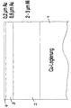
- the accompanying drawing shows schematically the typical structure of a bond flag, consisting of a carrier 1 made of a copper-based alloy, which is first nickel-plated in a conventional manner with a layer thickness of 2 to 3 ⁇ m; the nickel layer is designated by the reference number 2 and serves as a diffusion barrier between the copper alloy and the gold layer, which is applied in two steps according to the invention: in a first step, at a current density of 3 to 100 A / dm 2, preferably at a current density of 5 to 7 A / dm2, a 0.8 .mu.m thick gold layer 3, onto which a 0 in a second step at a lower current density, for example at 0.3 to 1 A / dm2, preferably at a current density of 0.6 A / dm2 , 2 ⁇ m thick surface layer 4 of gold is deposited.
- the separation takes place from a Fine gold bath of conventional composition, for example from a bath based on potassium gold cyanide or from a cyanide-free bath based
Landscapes
- Chemical & Material Sciences (AREA)
- Engineering & Computer Science (AREA)
- Chemical Kinetics & Catalysis (AREA)
- Electrochemistry (AREA)
- Materials Engineering (AREA)
- Metallurgy (AREA)
- Organic Chemistry (AREA)
- Electroplating Methods And Accessories (AREA)
- Battery Electrode And Active Subsutance (AREA)
Applications Claiming Priority (4)
| Application Number | Priority Date | Filing Date | Title |
|---|---|---|---|
| DE4426862 | 1994-07-28 | ||
| DE4426862 | 1994-07-28 | ||
| DE4436071A DE4436071C2 (de) | 1994-07-28 | 1994-10-10 | Verfahren zum Vergolden von bandförmigem Halbzeug, insbesondere für Leadframes und nach dem Verfahren vergoldete Leadframes |
| DE4436071 | 1994-10-10 |
Publications (3)
| Publication Number | Publication Date |
|---|---|
| EP0698677A2 true EP0698677A2 (fr) | 1996-02-28 |
| EP0698677A3 EP0698677A3 (fr) | 1998-08-26 |
| EP0698677B1 EP0698677B1 (fr) | 2002-10-09 |
Family
ID=25938782
Family Applications (1)
| Application Number | Title | Priority Date | Filing Date |
|---|---|---|---|
| EP95111826A Expired - Lifetime EP0698677B1 (fr) | 1994-07-28 | 1995-07-28 | Méthode pour le dorage de produits semi-finis en bandes, en particulier pour cadres de connexion |
Country Status (2)
| Country | Link |
|---|---|
| EP (1) | EP0698677B1 (fr) |
| ES (1) | ES2184776T3 (fr) |
Family Cites Families (3)
| Publication number | Priority date | Publication date | Assignee | Title |
|---|---|---|---|---|
| GB2147311B (en) * | 1983-09-29 | 1987-10-21 | Hara J B O | Electrodepositing precious metal alloys |
| DE3683595D1 (de) * | 1985-11-11 | 1992-03-05 | Electroplating Eng | Vorrichtung zum selektiven metallbeschichten von steckverbinderkontaktstiften. |
| DE3839223C2 (de) * | 1988-11-19 | 1994-10-20 | Degussa | Vorrichtung zur selektiven galvanischen Beschichtung |
-
1995
- 1995-07-28 ES ES95111826T patent/ES2184776T3/es not_active Expired - Lifetime
- 1995-07-28 EP EP95111826A patent/EP0698677B1/fr not_active Expired - Lifetime
Non-Patent Citations (1)
| Title |
|---|
| None |
Also Published As
| Publication number | Publication date |
|---|---|
| EP0698677B1 (fr) | 2002-10-09 |
| EP0698677A3 (fr) | 1998-08-26 |
| ES2184776T3 (es) | 2003-04-16 |
Similar Documents
| Publication | Publication Date | Title |
|---|---|---|
| DE3688840T2 (de) | Verfahren und vorrichtung zur elektroplattierung eines kupferblattes. | |
| DE19640256B4 (de) | Anschlußrahmen, Verfahren zur Edelmetallplattierung des Anschlußrahmens und Halbleitereinrichtung mit Anschlußrahmen | |
| DE69025500T2 (de) | Verfahren zur Herstellung eines kupferkaschierten Laminats | |
| DE2419157C3 (de) | Metallischer Träger für Halbleiterbauelemente und Verfahren zu seiner Herstellung | |
| DE69023858T2 (de) | Integrierte Schaltungsanordnung mit verbesserten Verbindungen zwischen den Steckerstiften und den Halbleitermaterial-Chips. | |
| DE3305952A1 (de) | Verfahren zum anbringen einer platte mit integrierter schaltung auf einem substrat | |
| DE69003333T2 (de) | Thermokompressionsverbindung für I.C.-Verpackung. | |
| DE102004019877A1 (de) | Klebeschicht zum Kleben von Harz auf eine Kupferoberfläche | |
| CH664107A5 (de) | Elektrode fuer drahtschneide-funkenerosion. | |
| DE3312713A1 (de) | Silberbeschichtete elektrische materialien und verfahren zu ihrer herstellung | |
| DE10136890B4 (de) | Verfahren und Vorrichtung zum Erzeugen eines kristallstrukturell texturierten Bandes aus Metall sowie Band | |
| DE3100634A1 (de) | "vorrichtung zum galvanisieren eines bands" | |
| EP0698677B1 (fr) | Méthode pour le dorage de produits semi-finis en bandes, en particulier pour cadres de connexion | |
| DE4436071C2 (de) | Verfahren zum Vergolden von bandförmigem Halbzeug, insbesondere für Leadframes und nach dem Verfahren vergoldete Leadframes | |
| DE4123911C1 (fr) | ||
| CH635871A5 (de) | Verfahren zum teilgalvanisieren. | |
| DE3618751A1 (de) | Kupferband (leiterrahmenband) | |
| DE3151557C2 (fr) | ||
| EP0859071B1 (fr) | Procédé de revêtement sélectif galvanique d'éléments de contact électrique | |
| EP0088220B1 (fr) | Elément de contact et méthode pour sa fabrication | |
| DE3029277C2 (de) | Aufbau von Metallschichten | |
| WO2001086018A2 (fr) | Procede de fabrication de pieces qui servent a conduire du courant electrique et qui sont couvertes d'une matiere principalement metallique | |
| DE102019119348B4 (de) | Beschichtetes Trägerband und Verwendung desselben zum Bonden einer Leistungselektronik | |
| DD273862A5 (de) | Kupferfolie mit zweiseitiger matter oberflaeche und verfahren zur herstellung einer kupfefolie | |
| DE2730625A1 (de) | Verfahren zur herstellung von stark verzinnten kupferdraehten |
Legal Events
| Date | Code | Title | Description |
|---|---|---|---|
| PUAI | Public reference made under article 153(3) epc to a published international application that has entered the european phase |
Free format text: ORIGINAL CODE: 0009012 |
|
| AK | Designated contracting states |
Kind code of ref document: A2 Designated state(s): DE DK ES FR GB IT SE |
|
| RAP1 | Party data changed (applicant data changed or rights of an application transferred) |
Owner name: DODUCO GMBH + CO DR. EUGEN DUERRWAECHTER I.K. |
|
| RAP1 | Party data changed (applicant data changed or rights of an application transferred) |
Owner name: DODUCO GMBH |
|
| PUAL | Search report despatched |
Free format text: ORIGINAL CODE: 0009013 |
|
| AK | Designated contracting states |
Kind code of ref document: A3 Designated state(s): DE DK ES FR GB IT SE |
|
| 17P | Request for examination filed |
Effective date: 19981005 |
|
| RAP1 | Party data changed (applicant data changed or rights of an application transferred) |
Owner name: AMI DODUCO GMBH |
|
| 17Q | First examination report despatched |
Effective date: 19991026 |
|
| GRAG | Despatch of communication of intention to grant |
Free format text: ORIGINAL CODE: EPIDOS AGRA |
|
| GRAG | Despatch of communication of intention to grant |
Free format text: ORIGINAL CODE: EPIDOS AGRA |
|
| GRAH | Despatch of communication of intention to grant a patent |
Free format text: ORIGINAL CODE: EPIDOS IGRA |
|
| GRAH | Despatch of communication of intention to grant a patent |
Free format text: ORIGINAL CODE: EPIDOS IGRA |
|
| GRAA | (expected) grant |
Free format text: ORIGINAL CODE: 0009210 |
|
| AK | Designated contracting states |
Kind code of ref document: B1 Designated state(s): DE DK ES FR GB IT SE |
|
| REG | Reference to a national code |
Ref country code: GB Ref legal event code: FG4D Free format text: NOT ENGLISH |
|
| REF | Corresponds to: |
Ref document number: 59510414 Country of ref document: DE Date of ref document: 20021114 |
|
| PG25 | Lapsed in a contracting state [announced via postgrant information from national office to epo] |
Ref country code: SE Free format text: LAPSE BECAUSE OF FAILURE TO SUBMIT A TRANSLATION OF THE DESCRIPTION OR TO PAY THE FEE WITHIN THE PRESCRIBED TIME-LIMIT Effective date: 20030109 Ref country code: DK Free format text: LAPSE BECAUSE OF FAILURE TO SUBMIT A TRANSLATION OF THE DESCRIPTION OR TO PAY THE FEE WITHIN THE PRESCRIBED TIME-LIMIT Effective date: 20030109 |
|
| GBT | Gb: translation of ep patent filed (gb section 77(6)(a)/1977) |
Effective date: 20030120 |
|
| ET | Fr: translation filed | ||
| REG | Reference to a national code |
Ref country code: ES Ref legal event code: FG2A Ref document number: 2184776 Country of ref document: ES Kind code of ref document: T3 |
|
| PLBE | No opposition filed within time limit |
Free format text: ORIGINAL CODE: 0009261 |
|
| STAA | Information on the status of an ep patent application or granted ep patent |
Free format text: STATUS: NO OPPOSITION FILED WITHIN TIME LIMIT |
|
| 26N | No opposition filed |
Effective date: 20030710 |
|
| PGFP | Annual fee paid to national office [announced via postgrant information from national office to epo] |
Ref country code: GB Payment date: 20050628 Year of fee payment: 11 |
|
| PGFP | Annual fee paid to national office [announced via postgrant information from national office to epo] |
Ref country code: DE Payment date: 20050701 Year of fee payment: 11 |
|
| PGFP | Annual fee paid to national office [announced via postgrant information from national office to epo] |
Ref country code: FR Payment date: 20050719 Year of fee payment: 11 |
|
| PGFP | Annual fee paid to national office [announced via postgrant information from national office to epo] |
Ref country code: ES Payment date: 20050721 Year of fee payment: 11 |
|
| PG25 | Lapsed in a contracting state [announced via postgrant information from national office to epo] |
Ref country code: GB Free format text: LAPSE BECAUSE OF NON-PAYMENT OF DUE FEES Effective date: 20060728 |
|
| PGFP | Annual fee paid to national office [announced via postgrant information from national office to epo] |
Ref country code: IT Payment date: 20060731 Year of fee payment: 12 |
|
| PG25 | Lapsed in a contracting state [announced via postgrant information from national office to epo] |
Ref country code: DE Free format text: LAPSE BECAUSE OF NON-PAYMENT OF DUE FEES Effective date: 20070201 |
|
| GBPC | Gb: european patent ceased through non-payment of renewal fee |
Effective date: 20060728 |
|
| REG | Reference to a national code |
Ref country code: FR Ref legal event code: ST Effective date: 20070330 |
|
| REG | Reference to a national code |
Ref country code: ES Ref legal event code: FD2A Effective date: 20060729 |
|
| PG25 | Lapsed in a contracting state [announced via postgrant information from national office to epo] |
Ref country code: ES Free format text: LAPSE BECAUSE OF NON-PAYMENT OF DUE FEES Effective date: 20060729 |
|
| PG25 | Lapsed in a contracting state [announced via postgrant information from national office to epo] |
Ref country code: FR Free format text: LAPSE BECAUSE OF NON-PAYMENT OF DUE FEES Effective date: 20060731 |
|
| PG25 | Lapsed in a contracting state [announced via postgrant information from national office to epo] |
Ref country code: IT Free format text: LAPSE BECAUSE OF NON-PAYMENT OF DUE FEES Effective date: 20070728 |