EP0698677B1 - Méthode pour le dorage de produits semi-finis en bandes, en particulier pour cadres de connexion - Google Patents
Méthode pour le dorage de produits semi-finis en bandes, en particulier pour cadres de connexion Download PDFInfo
- Publication number
- EP0698677B1 EP0698677B1 EP95111826A EP95111826A EP0698677B1 EP 0698677 B1 EP0698677 B1 EP 0698677B1 EP 95111826 A EP95111826 A EP 95111826A EP 95111826 A EP95111826 A EP 95111826A EP 0698677 B1 EP0698677 B1 EP 0698677B1
- Authority
- EP
- European Patent Office
- Prior art keywords
- gold
- current density
- layer
- thickness
- leadframes
- Prior art date
- Legal status (The legal status is an assumption and is not a legal conclusion. Google has not performed a legal analysis and makes no representation as to the accuracy of the status listed.)
- Expired - Lifetime
Links
- PCHJSUWPFVWCPO-UHFFFAOYSA-N gold Chemical compound [Au] PCHJSUWPFVWCPO-UHFFFAOYSA-N 0.000 title claims description 39
- 239000010931 gold Substances 0.000 title claims description 39
- 229910052737 gold Inorganic materials 0.000 title claims description 39
- 238000000034 method Methods 0.000 title claims description 13
- 238000007747 plating Methods 0.000 title claims description 5
- 239000000463 material Substances 0.000 title 1
- 239000011265 semifinished product Substances 0.000 claims description 8
- 239000004065 semiconductor Substances 0.000 claims description 3
- 239000010410 layer Substances 0.000 description 22
- PXHVJJICTQNCMI-UHFFFAOYSA-N Nickel Chemical compound [Ni] PXHVJJICTQNCMI-UHFFFAOYSA-N 0.000 description 4
- 230000008021 deposition Effects 0.000 description 4
- 239000002344 surface layer Substances 0.000 description 4
- 238000004519 manufacturing process Methods 0.000 description 3
- 239000000126 substance Substances 0.000 description 3
- 239000011248 coating agent Substances 0.000 description 2
- 238000000576 coating method Methods 0.000 description 2
- 238000011161 development Methods 0.000 description 2
- 230000018109 developmental process Effects 0.000 description 2
- 230000002349 favourable effect Effects 0.000 description 2
- 239000000203 mixture Substances 0.000 description 2
- 229910052759 nickel Inorganic materials 0.000 description 2
- 238000000926 separation method Methods 0.000 description 2
- RYGMFSIKBFXOCR-UHFFFAOYSA-N Copper Chemical compound [Cu] RYGMFSIKBFXOCR-UHFFFAOYSA-N 0.000 description 1
- 229910000881 Cu alloy Inorganic materials 0.000 description 1
- 229910045601 alloy Inorganic materials 0.000 description 1
- 239000000956 alloy Substances 0.000 description 1
- NHFMFALCHGVCPP-UHFFFAOYSA-M azanium;gold(1+);sulfite Chemical compound [NH4+].[Au+].[O-]S([O-])=O NHFMFALCHGVCPP-UHFFFAOYSA-M 0.000 description 1
- 230000004888 barrier function Effects 0.000 description 1
- 238000004140 cleaning Methods 0.000 description 1
- 239000004020 conductor Substances 0.000 description 1
- 229910052802 copper Inorganic materials 0.000 description 1
- 239000010949 copper Substances 0.000 description 1
- 230000007547 defect Effects 0.000 description 1
- 230000001419 dependent effect Effects 0.000 description 1
- 238000009792 diffusion process Methods 0.000 description 1
- 238000009713 electroplating Methods 0.000 description 1
- 239000007788 liquid Substances 0.000 description 1
- 230000000873 masking effect Effects 0.000 description 1
- 229910052751 metal Inorganic materials 0.000 description 1
- 239000002184 metal Substances 0.000 description 1
- XTFKWYDMKGAZKK-UHFFFAOYSA-N potassium;gold(1+);dicyanide Chemical compound [K+].[Au+].N#[C-].N#[C-] XTFKWYDMKGAZKK-UHFFFAOYSA-N 0.000 description 1
- 238000004080 punching Methods 0.000 description 1
- 238000003466 welding Methods 0.000 description 1
Images
Classifications
-
- C—CHEMISTRY; METALLURGY
- C25—ELECTROLYTIC OR ELECTROPHORETIC PROCESSES; APPARATUS THEREFOR
- C25D—PROCESSES FOR THE ELECTROLYTIC OR ELECTROPHORETIC PRODUCTION OF COATINGS; ELECTROFORMING; APPARATUS THEREFOR
- C25D5/00—Electroplating characterised by the process; Pretreatment or after-treatment of workpieces
- C25D5/60—Electroplating characterised by the structure or texture of the layers
- C25D5/623—Porosity of the layers
-
- C—CHEMISTRY; METALLURGY
- C25—ELECTROLYTIC OR ELECTROPHORETIC PROCESSES; APPARATUS THEREFOR
- C25D—PROCESSES FOR THE ELECTROLYTIC OR ELECTROPHORETIC PRODUCTION OF COATINGS; ELECTROFORMING; APPARATUS THEREFOR
- C25D5/00—Electroplating characterised by the process; Pretreatment or after-treatment of workpieces
- C25D5/10—Electroplating with more than one layer of the same or of different metals
-
- C—CHEMISTRY; METALLURGY
- C25—ELECTROLYTIC OR ELECTROPHORETIC PROCESSES; APPARATUS THEREFOR
- C25D—PROCESSES FOR THE ELECTROLYTIC OR ELECTROPHORETIC PRODUCTION OF COATINGS; ELECTROFORMING; APPARATUS THEREFOR
- C25D5/00—Electroplating characterised by the process; Pretreatment or after-treatment of workpieces
- C25D5/60—Electroplating characterised by the structure or texture of the layers
- C25D5/605—Surface topography of the layers, e.g. rough, dendritic or nodular layers
Definitions
- the invention relates to a method for continuous, selective, galvanic gold plating of band-shaped semi-finished products, especially for lead frames for semiconductor technology.
- bond flags their surface e.g. bondable through galvanic gold plating is. Bonding is a friction welding process with which thin wires are connected to the flags.
- the requirements for galvanic gold plating are e.g. in the MIL specif. G-45204B.
- the Gold layer on which is bonded is usually from high-purity fine gold baths on a nickel underlayer deposited.
- the present invention is based on the object to show you a way how to do it under mass production conditions, namely when running at high speed Strip electroplating, reliable in terms of quality higher quality bondable surfaces, which is more reliable Enable bond connections.
- the semi-finished product is in a first Step with a gold bath at higher current density and then in a further step with a gold bath treated at a lower current density. It has it has been shown that this is how gold surfaces receives, which are ideal for wire bonding and failures are much less common with bond connections to lead. It is another great advantage of the invention Process that the surface properties the gold layer regardless of its volume properties can be adjusted. That means but in no way that it depends on the bondability alone the surface properties would matter. The surface properties and the volume properties of the gold layer rather influence both in combination the bondability.
- the bondability determines first Line through its surface structure, roughness, the Friction coefficient to the bond wire and also by their Purity. Volume properties and surface properties can be set independently and thereby the bondability can be optimized. Fortunately, is deposited with a high current density Not only to deposit gold layer economically, but also has a low low for bonding Hardness. The disadvantage here is that at high Speed more unwanted foreign substances also deposited and embedded in the gold layer and that the layer is more porous than a slow one, gold layer deposited with low current density. The one deposited at low speed In contrast, the surface layer is denser, has fewer defects and is characterized by less Foreign inclusions from what is favorable for bonding, and shows another friction behavior that is more favorable for bonding.
- the current density with which the lower sub-layer deposits is preferably around one Factor 10 to 30 over the current density with which the thinner surface layer is deposited.
- the deposition can take place in such a way that the band-shaped Semi-finished product passes through the same bath twice, the bathroom the first time with high and operated the second time with low current density becomes. But it is also quite possible to use the band-shaped Semi-finished products in a gear two in a row arranged to pass through gold baths, whereby the gold baths have the same chemical composition, for the targeted adjustment of layer properties, however can also be composed differently.
- Coating apparatus are suitable e.g.
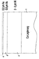
- the attached drawing shows schematically the typical structure of a bond flag, consisting of a carrier 1 made of a copper-based alloy, which is first nickel-plated in a conventional manner with a layer thickness of 2 to 3 ⁇ m; the nickel layer is designated by the reference number 2 and serves as a diffusion barrier between the copper alloy and the gold layer, which is applied in two steps according to the invention: in a first step at a current density of 3 to 100 A / dm 2 , preferably at a current density of 5 up to 7 A / dm 2 , a 0.8 ⁇ m thick gold layer 3 is formed, onto which in a second step at a lower current density, for example at 0.3 to 1 A / dm 2 , preferably at a current density of 0.6 A / dm 2, a 0.2 ⁇ m thick surface layer 4 made of gold is deposited.
- the deposition takes place from a fine gold bath of the usual composition, for example from a bath based on potassium gold cyanide or from a cyanide
Landscapes
- Chemical & Material Sciences (AREA)
- Engineering & Computer Science (AREA)
- Chemical Kinetics & Catalysis (AREA)
- Electrochemistry (AREA)
- Materials Engineering (AREA)
- Metallurgy (AREA)
- Organic Chemistry (AREA)
- Electroplating Methods And Accessories (AREA)
- Battery Electrode And Active Subsutance (AREA)
Claims (11)
- Procédé pour la dorure galvanique, sélective, continue de produits semi-finis en forme de rubans, en particulier pour des micropoutres pour la technologie des semi-conducteurs, caractérisé en ce que le produit semi-fini est traité dans une première étape avec un bain d'or à une densité de courant supérieure et ensuite dans une étape ultérieure avec un bain d'or à une densité de courant inférieure.
- Procédé selon la revendication 1, caractérisé en ce que la majeure partie de la couche d'or est réalisée avec la densité de courant supérieure.
- Procédé selon la revendication 1, caractérisé en ce qu'on obtient de 75 % à 90 % de l'épaisseur de la couche d'or avec la densité de courant supérieure.
- Procédé selon la revendication 1, caractérisé en ce qu'on obtient au maximum 0,4 µm, de préférence seulement 0,2 µm de l'épaisseur de la couche d'or avec la densité de courant inférieure.
- Procédé selon l'une quelconque des revendications précédentes, caractérisé en ce que les deux bains d'or utilisés dans les deux étapes sont identiques.
- Procédé selon la revendication 1, caractérisé en ce que, dans la première étape, la densité de courant se situe entre 3 A/dm2 et 100 A/dm2 et dans la deuxième étape la densité de courant se situe entre 0,3 A/dm2 et 1 A/dm2.
- Procédé selon la revendication 1, caractérisé en ce que, dans la première étape la densité de courant se situe entre 3 A/dm2 et 10 A/dm2 et dans la deuxième étape la densité de courant se situe entre 0,3 A/dm2 et 1 A/dm2.
- Micropoutre soumise à une dorure sélective pour la technologie des semi-conducteurs, caractérisée en ce que la couche d'or dans la couche partielle située à la surface présente une pureté supérieure et/ou une dureté supérieure à celles de la couche partielle sous-jacente, et en ce que les deux couches partielles de la couche d'or sont constituées d'or fin.
- Micropoutre selon la revendication 6, 7 ou 8, caractérisée en ce que la couche partielle située à la surface possède une épaisseur maximale de 0,3 µm, de préférence de seulement 0,2 µm.
- Micropoutre selon la revendication 8, caractérisée en ce que la couche partielle située à la surface représente de 10 % à 25 % de l'épaisseur de la couche d'or totale.
- Micropoutre selon l'une quelconque des revendications 8 à 10, caractérisée en ce que la couche partielle supérieure possède une épaisseur entre 0,15 et 0,4 µm, et la couche partielle inférieure possède une épaisseur entre 0,6 et 1,2 µm.
Applications Claiming Priority (4)
| Application Number | Priority Date | Filing Date | Title |
|---|---|---|---|
| DE4426862 | 1994-07-28 | ||
| DE4426862 | 1994-07-28 | ||
| DE4436071A DE4436071C2 (de) | 1994-07-28 | 1994-10-10 | Verfahren zum Vergolden von bandförmigem Halbzeug, insbesondere für Leadframes und nach dem Verfahren vergoldete Leadframes |
| DE4436071 | 1994-10-10 |
Publications (3)
| Publication Number | Publication Date |
|---|---|
| EP0698677A2 EP0698677A2 (fr) | 1996-02-28 |
| EP0698677A3 EP0698677A3 (fr) | 1998-08-26 |
| EP0698677B1 true EP0698677B1 (fr) | 2002-10-09 |
Family
ID=25938782
Family Applications (1)
| Application Number | Title | Priority Date | Filing Date |
|---|---|---|---|
| EP95111826A Expired - Lifetime EP0698677B1 (fr) | 1994-07-28 | 1995-07-28 | Méthode pour le dorage de produits semi-finis en bandes, en particulier pour cadres de connexion |
Country Status (2)
| Country | Link |
|---|---|
| EP (1) | EP0698677B1 (fr) |
| ES (1) | ES2184776T3 (fr) |
Family Cites Families (3)
| Publication number | Priority date | Publication date | Assignee | Title |
|---|---|---|---|---|
| GB2147311B (en) * | 1983-09-29 | 1987-10-21 | Hara J B O | Electrodepositing precious metal alloys |
| DE3683595D1 (de) * | 1985-11-11 | 1992-03-05 | Electroplating Eng | Vorrichtung zum selektiven metallbeschichten von steckverbinderkontaktstiften. |
| DE3839223C2 (de) * | 1988-11-19 | 1994-10-20 | Degussa | Vorrichtung zur selektiven galvanischen Beschichtung |
-
1995
- 1995-07-28 ES ES95111826T patent/ES2184776T3/es not_active Expired - Lifetime
- 1995-07-28 EP EP95111826A patent/EP0698677B1/fr not_active Expired - Lifetime
Also Published As
| Publication number | Publication date |
|---|---|
| EP0698677A3 (fr) | 1998-08-26 |
| ES2184776T3 (es) | 2003-04-16 |
| EP0698677A2 (fr) | 1996-02-28 |
Similar Documents
| Publication | Publication Date | Title |
|---|---|---|
| DE19640256B4 (de) | Anschlußrahmen, Verfahren zur Edelmetallplattierung des Anschlußrahmens und Halbleitereinrichtung mit Anschlußrahmen | |
| DE69723327T2 (de) | Elektrolytische Kupferfolie für eine gedruckte Schaltungsplatte und verfahren zu ihrer Herstellung | |
| DE69025500T2 (de) | Verfahren zur Herstellung eines kupferkaschierten Laminats | |
| DE102006017042B4 (de) | Zuleitungsrahmen für ein Halbleiterbauteil | |
| DE2419157C3 (de) | Metallischer Träger für Halbleiterbauelemente und Verfahren zu seiner Herstellung | |
| DE3417541C2 (de) | Verfahren zur Herstellung eines isolierten rechteckigen Drahtes | |
| DE69023858T2 (de) | Integrierte Schaltungsanordnung mit verbesserten Verbindungen zwischen den Steckerstiften und den Halbleitermaterial-Chips. | |
| EP0621633A2 (fr) | Cadre de connexion pour circuits intégrés | |
| DE69003333T2 (de) | Thermokompressionsverbindung für I.C.-Verpackung. | |
| DE3305952A1 (de) | Verfahren zum anbringen einer platte mit integrierter schaltung auf einem substrat | |
| EP0698677B1 (fr) | Méthode pour le dorage de produits semi-finis en bandes, en particulier pour cadres de connexion | |
| CH664107A5 (de) | Elektrode fuer drahtschneide-funkenerosion. | |
| DE4431847C5 (de) | Substrat mit bondfähiger Beschichtung | |
| DE4436071C2 (de) | Verfahren zum Vergolden von bandförmigem Halbzeug, insbesondere für Leadframes und nach dem Verfahren vergoldete Leadframes | |
| DE4123911C1 (fr) | ||
| DE4425943B4 (de) | Verfahren zur Herstellung eines mehrschichtigen Leiter- bzw. Anschlusselements und Leiter- bzw. Anschlusselement | |
| DE3618751A1 (de) | Kupferband (leiterrahmenband) | |
| DE3704200C2 (fr) | ||
| DE19962431A1 (de) | Verfahren zum Herstellen einer Halbleiteranordnung | |
| EP3105786A1 (fr) | Procédé de réalisation d'un revêtement soudable sur une bande substrat | |
| DE69533866T2 (de) | Leiterrahmen und Leiterrahmenmaterial | |
| EP0966045B1 (fr) | Procédé de fabrication d'une électrode métallique dans un dispositif semi-conducteur avec un transistor MOS | |
| DE4409340C2 (de) | Verfahren zur Herstellung einer Nut oder eines Kanals | |
| DE19827521C1 (de) | Verfahren zur Herstellung einer gebondeten, aluminiumhaltiges Material enthaltenden Vorrichtung | |
| DE7026304U (de) | Halbleiterscheibe mit vorgeformten goldenen loetbereichen. |
Legal Events
| Date | Code | Title | Description |
|---|---|---|---|
| PUAI | Public reference made under article 153(3) epc to a published international application that has entered the european phase |
Free format text: ORIGINAL CODE: 0009012 |
|
| AK | Designated contracting states |
Kind code of ref document: A2 Designated state(s): DE DK ES FR GB IT SE |
|
| RAP1 | Party data changed (applicant data changed or rights of an application transferred) |
Owner name: DODUCO GMBH + CO DR. EUGEN DUERRWAECHTER I.K. |
|
| RAP1 | Party data changed (applicant data changed or rights of an application transferred) |
Owner name: DODUCO GMBH |
|
| PUAL | Search report despatched |
Free format text: ORIGINAL CODE: 0009013 |
|
| AK | Designated contracting states |
Kind code of ref document: A3 Designated state(s): DE DK ES FR GB IT SE |
|
| 17P | Request for examination filed |
Effective date: 19981005 |
|
| RAP1 | Party data changed (applicant data changed or rights of an application transferred) |
Owner name: AMI DODUCO GMBH |
|
| 17Q | First examination report despatched |
Effective date: 19991026 |
|
| GRAG | Despatch of communication of intention to grant |
Free format text: ORIGINAL CODE: EPIDOS AGRA |
|
| GRAG | Despatch of communication of intention to grant |
Free format text: ORIGINAL CODE: EPIDOS AGRA |
|
| GRAH | Despatch of communication of intention to grant a patent |
Free format text: ORIGINAL CODE: EPIDOS IGRA |
|
| GRAH | Despatch of communication of intention to grant a patent |
Free format text: ORIGINAL CODE: EPIDOS IGRA |
|
| GRAA | (expected) grant |
Free format text: ORIGINAL CODE: 0009210 |
|
| AK | Designated contracting states |
Kind code of ref document: B1 Designated state(s): DE DK ES FR GB IT SE |
|
| REG | Reference to a national code |
Ref country code: GB Ref legal event code: FG4D Free format text: NOT ENGLISH |
|
| REF | Corresponds to: |
Ref document number: 59510414 Country of ref document: DE Date of ref document: 20021114 |
|
| PG25 | Lapsed in a contracting state [announced via postgrant information from national office to epo] |
Ref country code: SE Free format text: LAPSE BECAUSE OF FAILURE TO SUBMIT A TRANSLATION OF THE DESCRIPTION OR TO PAY THE FEE WITHIN THE PRESCRIBED TIME-LIMIT Effective date: 20030109 Ref country code: DK Free format text: LAPSE BECAUSE OF FAILURE TO SUBMIT A TRANSLATION OF THE DESCRIPTION OR TO PAY THE FEE WITHIN THE PRESCRIBED TIME-LIMIT Effective date: 20030109 |
|
| GBT | Gb: translation of ep patent filed (gb section 77(6)(a)/1977) |
Effective date: 20030120 |
|
| ET | Fr: translation filed | ||
| REG | Reference to a national code |
Ref country code: ES Ref legal event code: FG2A Ref document number: 2184776 Country of ref document: ES Kind code of ref document: T3 |
|
| PLBE | No opposition filed within time limit |
Free format text: ORIGINAL CODE: 0009261 |
|
| STAA | Information on the status of an ep patent application or granted ep patent |
Free format text: STATUS: NO OPPOSITION FILED WITHIN TIME LIMIT |
|
| 26N | No opposition filed |
Effective date: 20030710 |
|
| PGFP | Annual fee paid to national office [announced via postgrant information from national office to epo] |
Ref country code: GB Payment date: 20050628 Year of fee payment: 11 |
|
| PGFP | Annual fee paid to national office [announced via postgrant information from national office to epo] |
Ref country code: DE Payment date: 20050701 Year of fee payment: 11 |
|
| PGFP | Annual fee paid to national office [announced via postgrant information from national office to epo] |
Ref country code: FR Payment date: 20050719 Year of fee payment: 11 |
|
| PGFP | Annual fee paid to national office [announced via postgrant information from national office to epo] |
Ref country code: ES Payment date: 20050721 Year of fee payment: 11 |
|
| PG25 | Lapsed in a contracting state [announced via postgrant information from national office to epo] |
Ref country code: GB Free format text: LAPSE BECAUSE OF NON-PAYMENT OF DUE FEES Effective date: 20060728 |
|
| PGFP | Annual fee paid to national office [announced via postgrant information from national office to epo] |
Ref country code: IT Payment date: 20060731 Year of fee payment: 12 |
|
| PG25 | Lapsed in a contracting state [announced via postgrant information from national office to epo] |
Ref country code: DE Free format text: LAPSE BECAUSE OF NON-PAYMENT OF DUE FEES Effective date: 20070201 |
|
| GBPC | Gb: european patent ceased through non-payment of renewal fee |
Effective date: 20060728 |
|
| REG | Reference to a national code |
Ref country code: FR Ref legal event code: ST Effective date: 20070330 |
|
| REG | Reference to a national code |
Ref country code: ES Ref legal event code: FD2A Effective date: 20060729 |
|
| PG25 | Lapsed in a contracting state [announced via postgrant information from national office to epo] |
Ref country code: ES Free format text: LAPSE BECAUSE OF NON-PAYMENT OF DUE FEES Effective date: 20060729 |
|
| PG25 | Lapsed in a contracting state [announced via postgrant information from national office to epo] |
Ref country code: FR Free format text: LAPSE BECAUSE OF NON-PAYMENT OF DUE FEES Effective date: 20060731 |
|
| PG25 | Lapsed in a contracting state [announced via postgrant information from national office to epo] |
Ref country code: IT Free format text: LAPSE BECAUSE OF NON-PAYMENT OF DUE FEES Effective date: 20070728 |