EP0698677B1 - Method for gold plating of stripped material, especially for leadframes - Google Patents
Method for gold plating of stripped material, especially for leadframes Download PDFInfo
- Publication number
- EP0698677B1 EP0698677B1 EP95111826A EP95111826A EP0698677B1 EP 0698677 B1 EP0698677 B1 EP 0698677B1 EP 95111826 A EP95111826 A EP 95111826A EP 95111826 A EP95111826 A EP 95111826A EP 0698677 B1 EP0698677 B1 EP 0698677B1
- Authority
- EP
- European Patent Office
- Prior art keywords
- gold
- current density
- layer
- thickness
- leadframes
- Prior art date
- Legal status (The legal status is an assumption and is not a legal conclusion. Google has not performed a legal analysis and makes no representation as to the accuracy of the status listed.)
- Expired - Lifetime
Links
- PCHJSUWPFVWCPO-UHFFFAOYSA-N gold Chemical compound [Au] PCHJSUWPFVWCPO-UHFFFAOYSA-N 0.000 title claims description 39
- 239000010931 gold Substances 0.000 title claims description 39
- 229910052737 gold Inorganic materials 0.000 title claims description 39
- 238000000034 method Methods 0.000 title claims description 13
- 238000007747 plating Methods 0.000 title claims description 5
- 239000000463 material Substances 0.000 title 1
- 239000011265 semifinished product Substances 0.000 claims description 8
- 239000004065 semiconductor Substances 0.000 claims description 3
- 239000010410 layer Substances 0.000 description 22
- PXHVJJICTQNCMI-UHFFFAOYSA-N Nickel Chemical compound [Ni] PXHVJJICTQNCMI-UHFFFAOYSA-N 0.000 description 4
- 230000008021 deposition Effects 0.000 description 4
- 239000002344 surface layer Substances 0.000 description 4
- 238000004519 manufacturing process Methods 0.000 description 3
- 239000000126 substance Substances 0.000 description 3
- 239000011248 coating agent Substances 0.000 description 2
- 238000000576 coating method Methods 0.000 description 2
- 238000011161 development Methods 0.000 description 2
- 230000018109 developmental process Effects 0.000 description 2
- 230000002349 favourable effect Effects 0.000 description 2
- 239000000203 mixture Substances 0.000 description 2
- 229910052759 nickel Inorganic materials 0.000 description 2
- 238000000926 separation method Methods 0.000 description 2
- RYGMFSIKBFXOCR-UHFFFAOYSA-N Copper Chemical compound [Cu] RYGMFSIKBFXOCR-UHFFFAOYSA-N 0.000 description 1
- 229910000881 Cu alloy Inorganic materials 0.000 description 1
- 229910045601 alloy Inorganic materials 0.000 description 1
- 239000000956 alloy Substances 0.000 description 1
- NHFMFALCHGVCPP-UHFFFAOYSA-M azanium;gold(1+);sulfite Chemical compound [NH4+].[Au+].[O-]S([O-])=O NHFMFALCHGVCPP-UHFFFAOYSA-M 0.000 description 1
- 230000004888 barrier function Effects 0.000 description 1
- 238000004140 cleaning Methods 0.000 description 1
- 239000004020 conductor Substances 0.000 description 1
- 229910052802 copper Inorganic materials 0.000 description 1
- 239000010949 copper Substances 0.000 description 1
- 230000007547 defect Effects 0.000 description 1
- 230000001419 dependent effect Effects 0.000 description 1
- 238000009792 diffusion process Methods 0.000 description 1
- 238000009713 electroplating Methods 0.000 description 1
- 239000007788 liquid Substances 0.000 description 1
- 230000000873 masking effect Effects 0.000 description 1
- 229910052751 metal Inorganic materials 0.000 description 1
- 239000002184 metal Substances 0.000 description 1
- XTFKWYDMKGAZKK-UHFFFAOYSA-N potassium;gold(1+);dicyanide Chemical compound [K+].[Au+].N#[C-].N#[C-] XTFKWYDMKGAZKK-UHFFFAOYSA-N 0.000 description 1
- 238000004080 punching Methods 0.000 description 1
- 238000003466 welding Methods 0.000 description 1
Images
Classifications
-
- C—CHEMISTRY; METALLURGY
- C25—ELECTROLYTIC OR ELECTROPHORETIC PROCESSES; APPARATUS THEREFOR
- C25D—PROCESSES FOR THE ELECTROLYTIC OR ELECTROPHORETIC PRODUCTION OF COATINGS; ELECTROFORMING; APPARATUS THEREFOR
- C25D5/00—Electroplating characterised by the process; Pretreatment or after-treatment of workpieces
- C25D5/60—Electroplating characterised by the structure or texture of the layers
- C25D5/623—Porosity of the layers
-
- C—CHEMISTRY; METALLURGY
- C25—ELECTROLYTIC OR ELECTROPHORETIC PROCESSES; APPARATUS THEREFOR
- C25D—PROCESSES FOR THE ELECTROLYTIC OR ELECTROPHORETIC PRODUCTION OF COATINGS; ELECTROFORMING; APPARATUS THEREFOR
- C25D5/00—Electroplating characterised by the process; Pretreatment or after-treatment of workpieces
- C25D5/10—Electroplating with more than one layer of the same or of different metals
-
- C—CHEMISTRY; METALLURGY
- C25—ELECTROLYTIC OR ELECTROPHORETIC PROCESSES; APPARATUS THEREFOR
- C25D—PROCESSES FOR THE ELECTROLYTIC OR ELECTROPHORETIC PRODUCTION OF COATINGS; ELECTROFORMING; APPARATUS THEREFOR
- C25D5/00—Electroplating characterised by the process; Pretreatment or after-treatment of workpieces
- C25D5/60—Electroplating characterised by the structure or texture of the layers
- C25D5/605—Surface topography of the layers, e.g. rough, dendritic or nodular layers
Definitions
- the invention relates to a method for continuous, selective, galvanic gold plating of band-shaped semi-finished products, especially for lead frames for semiconductor technology.
- bond flags their surface e.g. bondable through galvanic gold plating is. Bonding is a friction welding process with which thin wires are connected to the flags.
- the requirements for galvanic gold plating are e.g. in the MIL specif. G-45204B.
- the Gold layer on which is bonded is usually from high-purity fine gold baths on a nickel underlayer deposited.
- the present invention is based on the object to show you a way how to do it under mass production conditions, namely when running at high speed Strip electroplating, reliable in terms of quality higher quality bondable surfaces, which is more reliable Enable bond connections.
- the semi-finished product is in a first Step with a gold bath at higher current density and then in a further step with a gold bath treated at a lower current density. It has it has been shown that this is how gold surfaces receives, which are ideal for wire bonding and failures are much less common with bond connections to lead. It is another great advantage of the invention Process that the surface properties the gold layer regardless of its volume properties can be adjusted. That means but in no way that it depends on the bondability alone the surface properties would matter. The surface properties and the volume properties of the gold layer rather influence both in combination the bondability.
- the bondability determines first Line through its surface structure, roughness, the Friction coefficient to the bond wire and also by their Purity. Volume properties and surface properties can be set independently and thereby the bondability can be optimized. Fortunately, is deposited with a high current density Not only to deposit gold layer economically, but also has a low low for bonding Hardness. The disadvantage here is that at high Speed more unwanted foreign substances also deposited and embedded in the gold layer and that the layer is more porous than a slow one, gold layer deposited with low current density. The one deposited at low speed In contrast, the surface layer is denser, has fewer defects and is characterized by less Foreign inclusions from what is favorable for bonding, and shows another friction behavior that is more favorable for bonding.
- the current density with which the lower sub-layer deposits is preferably around one Factor 10 to 30 over the current density with which the thinner surface layer is deposited.
- the deposition can take place in such a way that the band-shaped Semi-finished product passes through the same bath twice, the bathroom the first time with high and operated the second time with low current density becomes. But it is also quite possible to use the band-shaped Semi-finished products in a gear two in a row arranged to pass through gold baths, whereby the gold baths have the same chemical composition, for the targeted adjustment of layer properties, however can also be composed differently.
- Coating apparatus are suitable e.g.
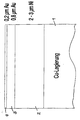
- the attached drawing shows schematically the typical structure of a bond flag, consisting of a carrier 1 made of a copper-based alloy, which is first nickel-plated in a conventional manner with a layer thickness of 2 to 3 ⁇ m; the nickel layer is designated by the reference number 2 and serves as a diffusion barrier between the copper alloy and the gold layer, which is applied in two steps according to the invention: in a first step at a current density of 3 to 100 A / dm 2 , preferably at a current density of 5 up to 7 A / dm 2 , a 0.8 ⁇ m thick gold layer 3 is formed, onto which in a second step at a lower current density, for example at 0.3 to 1 A / dm 2 , preferably at a current density of 0.6 A / dm 2, a 0.2 ⁇ m thick surface layer 4 made of gold is deposited.
- the deposition takes place from a fine gold bath of the usual composition, for example from a bath based on potassium gold cyanide or from a cyanide
Landscapes
- Chemical & Material Sciences (AREA)
- Engineering & Computer Science (AREA)
- Chemical Kinetics & Catalysis (AREA)
- Electrochemistry (AREA)
- Materials Engineering (AREA)
- Metallurgy (AREA)
- Organic Chemistry (AREA)
- Electroplating Methods And Accessories (AREA)
- Battery Electrode And Active Subsutance (AREA)
Description
Die Erfindung befaßt sich mit einem Verfahren zum fortlaufenden, selektiven, galvanischen Vergolden von bandförmigem Halbzeug, insbesondere für Leadframes für die Halbleitertechnologie.The invention relates to a method for continuous, selective, galvanic gold plating of band-shaped semi-finished products, especially for lead frames for semiconductor technology.
Bei elektronischen und mikromechanischen Bauelementen besteht häufig die Aufgabe, sie durch Drähte mit Leiterbahnen zu verbinden, die Bestandteil ihrer Träger oder Gehäuse sind. Dazu besitzen diese Leiterbahnen sogenannte Bondfahnen, deren Oberfläche z.B. durch galvanische Vergoldung bondbar ausgebildet ist. Das Bonden ist ein Reibschweißverfahren, mit welchem dünne Drähte mit den Bondfahnen verbunden werden. Die Anforderungen an die galvanische Vergoldung sind z.B. in der MIL-Specif. G-45204B festgelegt. Die Goldschicht, auf welcher gebondet wird, wird üblicherweise aus hochreinen Feingoldbädern auf einer Nickel-Unterschicht abgeschieden.For electronic and micromechanical components there is often the task of using them with wires Connect interconnects that are part of their Carrier or housing are. In addition, these have conductor tracks so-called bond flags, their surface e.g. bondable through galvanic gold plating is. Bonding is a friction welding process with which thin wires are connected to the flags. The requirements for galvanic gold plating are e.g. in the MIL specif. G-45204B. The Gold layer on which is bonded is usually from high-purity fine gold baths on a nickel underlayer deposited.
Trotz Erfüllung der MIL-Specification gibt es in der industriellen Serienfertigung immer wieder schwer zu erklärende Probleme mit der Festigkeit der Bondverbindungen.Despite meeting the MIL specification, there is in the industrial series production always difficult explanatory problems with the strength of the bond connections.
Der vorliegenden Erfindung liegt die Aufgabe zugrunde, einen Weg aufzuzeigen, wie man unter Serienfertigungsbedingungen, nämlich bei mit hoher Geschwindigkeit ablaufender Bandgalvanik, prozeßsicher zu qualitativ hochwertigeren bondbaren Oberflächen kommt, welche zuverlässigere Bondverbindungen ermöglichen.The present invention is based on the object to show you a way how to do it under mass production conditions, namely when running at high speed Strip electroplating, reliable in terms of quality higher quality bondable surfaces, which is more reliable Enable bond connections.
Diese Aufgabe wird gelöst durch ein Verfahren mit den im Anspruch 1 angegebenen Merkmalen. Vorteilhafte Weiterbildungen der Erfindung sind Gegenstand der abhängigen Ansprüche.This problem is solved by a method with the features specified in claim 1. advantageous Developments of the invention are the subject of the dependent Expectations.
Erfindungsgemäss wird das Halbzeug in einem ersten Schritt mit einem Goldbad bei höherer Stromdichte und danach in einem weiteren Schritt mit einem Goldbad bei einer niedrigeren Stromdichte behandelt. Es hat sich gezeigt, dass man auf diese Weise Goldoberflächen erhält, die sich hervorragend für das Drahtbonden eignen und bei den Bondverbindungen viel seltener zu Ausfällen führen. Es ist ein weiterer großer Vorteil des erfindungsgemässen Verfahrens, dass die Oberflächeneigenschaften der Goldschicht unabhängig von ihren Volumeneigenschaften eingestellt werden können. Das bedeutet aber keineswegs, dass es für die Bondbarkeit allein auf die Oberflächeneigenschaften ankäme. Die Oberflächeneigenschaften und die Volumeneigenschaften der Goldschicht beeinflussen vielmehr beide in Kombination die Bondbarkeit.According to the invention, the semi-finished product is in a first Step with a gold bath at higher current density and then in a further step with a gold bath treated at a lower current density. It has it has been shown that this is how gold surfaces receives, which are ideal for wire bonding and failures are much less common with bond connections to lead. It is another great advantage of the invention Process that the surface properties the gold layer regardless of its volume properties can be adjusted. That means but in no way that it depends on the bondability alone the surface properties would matter. The surface properties and the volume properties of the gold layer rather influence both in combination the bondability.
Beim Arbeiten mit niedrigerer Stromdichte erfolgt das Schichtwachstum nur langsam. Für eine rationelle Serienfertigung ist das unerwünscht. Beim Stand der Technik arbeitet man deshalb mit möglichst hoher Abscheidegeschwindigkeit und deshalb mit möglichst hoher Stromdichte (high speed-Bedingungen). Erfindungsgemäss führt die Anwendung eines Abscheideschrittes bei niedriger Stromdichte aber nicht dazu, dass das Verfahren unwirtschaftlich wird, weil der größte Teil des Schichtaufbaus nach wie vor bei hoher Stromdichte und deshalb bei entsprechend hoher Abscheidegeschwindigkeit erfolgt. Vorzugsweise werden etwa 75 bis 90% der Dicke der Goldschicht bei höherer Stromdichte erzeugt, lediglich der Rest bei niedriger Stromdichte; zahlenmässig ausgedrückt wird ein Schichtaufbau bevorzugt, bei welchem 0,6 bis 1,2 µm Gold bei hoher Stromdichte und 0,15 bis 0,4 µm Gold bei niedriger Stromdichte abgeschieden werden. Besonders bewährt hat sich ein Schichtaufbau, bei welchem 0,8 µm bei hoher Stromdichte und 0,2 µm bei niedriger Stromdichte abgeschieden werden.This happens when working with a lower current density Layer growth is slow. For efficient series production it is undesirable. In the state of the art therefore one works with the highest possible separation speed and therefore with the highest possible current density (high speed conditions). According to the invention leads the application of a deposition step at lower Current density does not make the process uneconomical is because most of the layer structure still with high current density and therefore at a correspondingly high separation speed. Preferably about 75 to 90% of the thickness of the gold layer generated at higher current density, only the Rest at low current density; in terms of numbers a layer structure is preferred in which 0.6 to 1.2 µm gold at high current density and 0.15 to 0.4 µm Gold can be deposited at low current density. A layer structure, in which 0.8 µm at high current density and 0.2 µm at low current density.
Bei einem erfindungsgemässen Aufbau der Goldschicht beeinflußt die zuerst abgeschiedene dickere Teilschicht die Bondbarkeit vor allem durch ihre Härte, Dicke und Reinheit, die als nächstes abgeschiedene Oberflächenschicht hingegen bestimmt die Bondbarkeit in erster Linie durch ihre Oberflächenstruktur, Rauhigkeit, den Reibungskoeffizienten zum Bonddraht und auch durch ihre Reinheit. Volumeneigenschaften und Oberflächeneigenschaften können unabhängig voneinander eingestellt und dadurch die Bondbarkeit optimiert werden. Erfreulicherweise ist eine mit hoher Stromdichte abgeschiedene Goldschicht nicht nur wirtschaftlich abzuscheiden, sondern hat auch eine für das Bonden günstige niedrige Härte. Nachteilig dabei ist jedoch, dass bei hoher Geschwindigkeit mehr unerwünschte Fremdsubstanzen mit abgeschieden und in die Goldschicht eingelagert werden und dass die Schicht poröser ist als eine langsam, mit niedriger Stromdichte abgeschiedene Goldschicht. Die mit niedriger Geschwindigkeit abgeschiedene Oberflächenschicht ist demgegenüber dichter, hat weniger Fehlstellen und zeichnet sich durch weniger Fremdeinschlüsse aus, was für das Bonden günstig ist, und zeigt ein anderes für das Bonden günstigeres Reibverhalten. When the gold layer is built up according to the invention affects the thicker partial layer deposited first the bondability mainly due to its hardness, thickness and Purity, the next deposited surface layer however, the bondability determines first Line through its surface structure, roughness, the Friction coefficient to the bond wire and also by their Purity. Volume properties and surface properties can be set independently and thereby the bondability can be optimized. Fortunately, is deposited with a high current density Not only to deposit gold layer economically, but also has a low low for bonding Hardness. The disadvantage here is that at high Speed more unwanted foreign substances also deposited and embedded in the gold layer and that the layer is more porous than a slow one, gold layer deposited with low current density. The one deposited at low speed In contrast, the surface layer is denser, has fewer defects and is characterized by less Foreign inclusions from what is favorable for bonding, and shows another friction behavior that is more favorable for bonding.
Die Stromdichte, mit welcher man die untere Teilschicht abscheidet, liegt vorzugsweise um einen Faktor 10 bis 30 über der Stromdichte, mit welcher die dünnere Oberflächenschicht abgeschieden wird. Die Abscheidung kann so erfolgen, dass das bandförmige Halbzeug ein und dasselbe Bad zweimal durchläuft, wobei das Bad beim ersten Mal mit hoher und beim zweiten Mal mit niedriger Stromdichte betrieben wird. Es ist aber auch durchaus möglich, das bandförmige Halbzeug in einem Gang zwei hintereinander angeordnete Goldbäder durchlaufen zu lassen, wobei die Goldbäder in der chemischen Zusammensetzung gleich, zur gezielten Einstellung von Schichteigenschaften aber auch unterschiedlich zusammengesetzt sein können. Als Beschichtungsapparat eignen sich z.B. die in der DE-A-40 19 643 offenbarte Vorrichtung zum Abscheiden von Goldstreifen auf Bänder aus Metall, wobei die Lage und Breite der Goldstreifen durch Maskenbänder bestimmt wird, oder ein Apparat zur Spotvergoldung, bei der auf einem zu beschichtenden Band ein mit diesem mitlaufendes Maskenband liegt, welches einzelne Fenster hat, die die Lage und Größe der abzuscheidenden Spots bestimmen. Ferner eignet sich der in der EP 370 239 dargestellte Beschichtungsapparat, welcher einen langgestreckten Düsenkopf hat, über welchen ein Filz gespannt ist, der mit der Goldbadflüssigkeit getränkt ist und über welchen das bandförmige Halbzeug zum selektiven Vergolden hinweggezogen wird. Schließlich sind auch Kombinationen der Arbeitsweisen mit den vorgenannten Apparaten möglich. The current density with which the lower sub-layer deposits, is preferably around one Factor 10 to 30 over the current density with which the thinner surface layer is deposited. The deposition can take place in such a way that the band-shaped Semi-finished product passes through the same bath twice, the bathroom the first time with high and operated the second time with low current density becomes. But it is also quite possible to use the band-shaped Semi-finished products in a gear two in a row arranged to pass through gold baths, whereby the gold baths have the same chemical composition, for the targeted adjustment of layer properties, however can also be composed differently. As Coating apparatus are suitable e.g. that in DE-A-40 19 643 disclosed apparatus for separating Gold stripes on metal bands, the location and Width of the gold stripes determined by masking tapes is, or a device for spot gilding, on the a belt to be coated with it Mask tape lies, which has individual windows, which determine the location and size of the spots to be separated. The one shown in EP 370 239 is also suitable Coating apparatus, which has an elongated Nozzle head, over which a felt is stretched which is soaked in the gold bath liquid and over which the band-shaped semi-finished product for selective gilding is pulled away. After all, there are also combinations the ways of working with the aforementioned Apparatus possible.
In vorteilhafter Weiterbildung des erfindungsgemässen Verfahrens ist es auch möglich, zwischen der mit hoher Stromdichte erfolgenden Abscheidung und der mit niedriger Stromdichte erfolgenden Abscheidung mechanische Bearbeitungen am Halbzeug vorzunehmen, z.B. Stanzvorgänge; Fremdsubstanzen, die dadurch auf oder in die Goldschicht gelangen und sich durch übliche Reinigungsverfahren nicht vollständig entfernen lassen, können durch die nachträgliche dünne Vergoldung, welche mit niedriger Stromdichte erfolgt, überdeckt werden, so dass auch in diesem Fall Goldschichten erhalten werden, die sich hervorragend zum Drahtbonden eignen.In an advantageous development of the inventive It is also possible to choose between those with high Current density and the lower Current-tight deposition mechanical processing on the semi-finished product, e.g. Punching operations; Foreign substances that are thereby on or in the Go gold layer and get through usual cleaning procedures cannot be removed completely through the subsequent thin gilding, which with low current density is covered, so that gold layers are obtained in this case too, which are ideal for wire bonding.
Die beigefügte Zeichnung zeigt schematisch den typischen
Aufbau einer Bondfahne, bestehend aus einem Träger 1
aus einer Kupfer-Basislegierung, welche zunächst auf
übliche Weise mit einer Schichtdicke von 2 bis 3 µm
vernickelt wird; die Nickelschicht ist mit der Bezugszahl
2 bezeichnet und dient als Diffusionsbarriere zwischen
der Kupferlegierung und der Goldschicht, welche
erfindungsgemäss in zwei Schritten aufgetragen wird:
In einem ersten Schritt wird bei einer Stromdichte von
3 bis 100 A/dm2, vorzugsweise bei einer Stromdichte von
5 bis 7 A/dm2, eine 0,8 µm dicke Goldschicht 3 gebildete,
auf welche in einem zweiten Schritt bei einer
niedrigeren Stromdichte, z.B. bei 0,3 bis 1 A/dm2,
vorzugsweise bei einer Stromdichte von 0,6 A/dm2
eine 0,2 µm dicke Oberflächenschicht 4 aus Gold abgeschieden
wird. Die Abscheidung erfolgt aus einem
Feingoldbad üblicher Zusammensetzung, z.B. aus einem
Bad auf Kalium-Goldzyanid-Basis oder aus einem zyanidfreien
Bad auf Ammonium-Goldsulfit-Basis.The attached drawing shows schematically the typical structure of a bond flag, consisting of a carrier 1 made of a copper-based alloy, which is first nickel-plated in a conventional manner with a layer thickness of 2 to 3 μm; the nickel layer is designated by the
Claims (11)
- Method for the continuous, selective, galvanic gold-plating of ribbonshaped semi-finished products, especially for leadframes for semiconductor technology,
characterised in that the semi-finished product is treated, in a first step, in a gold bath at higher current density and thereafter, in a further step, in a gold bath at lower current density. - The method as defined in Claim 1, characterised in that the larger part of the gold layer is produced at the higher current density.
- The method as defined in Claim 1, characterised in that 75 % to 90 % of the thickness of the gold layer is produced at the higher current density.
- The method as defined in Claim 1, characterised in that a maximum of 0.4 µm, preferably only 0.2 µm, of the thickness of the gold layer is produced at the lower current density.
- The method as defined in any of the preceding Claims, characterised in that the gold baths used for the two steps are identical.
- The method as defined in Claim 1, characterised in that the current density is between 3 A/dm2 and 100 A/dm2 in the first step and between 0.3 A/dm2 and 1 A/dm2 in the second step.
- The method as defined in Claim 1, characterised in that the current density is between 3 A/dm2 and 10 A/dm2 in the first step and between 0.3 A/dm2 and 1 A/dm2 in the second step.
- Selectively gold-plated leadframes for semiconductor technology, characterised in that the gold layer has a higher purity and/or a greater hardness in a partial layer near the surface, as compared with the lower partial layer, and that the two partial layers of the gold layer consist of fine gold.
- Leadframe as defined in Claim 6, 7 or 8, characterised in that the partial layer at the surface has a thickness of maximally 0.3 µm, preferably only 0.2 µm.
- Leadframe as defined in Claim 8, characterised in that the thickness of the partial layer at the surface is 10 % to 25 % of the thickness of the entire gold layer.
- Leadframe as defined in any of Claims 8 to 10, characterised in that the upper partial layer has a thickness of between 0.15 and 0.4 µm, while the lower partial layer has a thickness of between 0.6 and 1.2 µm.
Applications Claiming Priority (4)
| Application Number | Priority Date | Filing Date | Title |
|---|---|---|---|
| DE4426862 | 1994-07-28 | ||
| DE4426862 | 1994-07-28 | ||
| DE4436071A DE4436071C2 (en) | 1994-07-28 | 1994-10-10 | Process for gilding band-shaped semi-finished products, in particular for lead frames, and lead frames gold-plated according to the process |
| DE4436071 | 1994-10-10 |
Publications (3)
| Publication Number | Publication Date |
|---|---|
| EP0698677A2 EP0698677A2 (en) | 1996-02-28 |
| EP0698677A3 EP0698677A3 (en) | 1998-08-26 |
| EP0698677B1 true EP0698677B1 (en) | 2002-10-09 |
Family
ID=25938782
Family Applications (1)
| Application Number | Title | Priority Date | Filing Date |
|---|---|---|---|
| EP95111826A Expired - Lifetime EP0698677B1 (en) | 1994-07-28 | 1995-07-28 | Method for gold plating of stripped material, especially for leadframes |
Country Status (2)
| Country | Link |
|---|---|
| EP (1) | EP0698677B1 (en) |
| ES (1) | ES2184776T3 (en) |
Family Cites Families (3)
| Publication number | Priority date | Publication date | Assignee | Title |
|---|---|---|---|---|
| GB2147311B (en) * | 1983-09-29 | 1987-10-21 | Hara J B O | Electrodepositing precious metal alloys |
| EP0222232B1 (en) * | 1985-11-11 | 1992-01-22 | Electroplating Engineers of Japan Limited | Plating device for minute portions of connector terminals |
| DE3839223C2 (en) * | 1988-11-19 | 1994-10-20 | Degussa | Selective electroplating device |
-
1995
- 1995-07-28 EP EP95111826A patent/EP0698677B1/en not_active Expired - Lifetime
- 1995-07-28 ES ES95111826T patent/ES2184776T3/en not_active Expired - Lifetime
Also Published As
| Publication number | Publication date |
|---|---|
| EP0698677A3 (en) | 1998-08-26 |
| EP0698677A2 (en) | 1996-02-28 |
| ES2184776T3 (en) | 2003-04-16 |
Similar Documents
| Publication | Publication Date | Title |
|---|---|---|
| DE19640256B4 (en) | Lead frame, method for precious metal plating of the lead frame and semiconductor device with lead frame | |
| DE69723327T2 (en) | Electrolytic copper foil for a printed circuit board and process for its production | |
| DE69735588T2 (en) | MANUFACTURE OF A COMPONENT FOR A SEMICONDUCTOR CIRCUIT | |
| DE2419157C3 (en) | Metallic carrier for semiconductor components and process for its manufacture | |
| DE3417541C2 (en) | Method of making an insulated rectangular wire | |
| DE69023858T2 (en) | Integrated circuit arrangement with improved connections between the connector pins and the semiconductor material chips. | |
| EP0621633A2 (en) | Leadframe for integrated circuits | |
| DE3305952A1 (en) | Method of mounting an integrated circuit panel on a substrate | |
| DE10011368A1 (en) | Semiconductor device has copper-tin alloy layer formed on junction portion of solder ball consisting of tin, and wiring consisting of copper | |
| EP0698677B1 (en) | Method for gold plating of stripped material, especially for leadframes | |
| CH664107A5 (en) | ELECTRODE FOR WIRE CUTTING SPARK EDM. | |
| DE4431847C5 (en) | Substrate with bondable coating | |
| DE4436071C2 (en) | Process for gilding band-shaped semi-finished products, in particular for lead frames, and lead frames gold-plated according to the process | |
| DE4123911C1 (en) | ||
| DE4425943B4 (en) | Method for producing a multilayer conductor element or connecting element and conductor or connection element | |
| DE3618751A1 (en) | COPPER TAPE (LADDER FRAME TAPE) | |
| DE3704200C2 (en) | ||
| DE10222670B4 (en) | An electric device having a plurality of metal pads on which a metal wiring is bonded, and a manufacturing method thereof | |
| DE19962431A1 (en) | Method of manufacturing a semiconductor device | |
| EP0088220B1 (en) | Contact member and method for its manufacture | |
| DE3047671C2 (en) | Process for the continuous molten coating of metal parts with a solderable layer of tin or tin-lead alloy and apparatus for carrying out such a process | |
| DE69533866T2 (en) | Lead frame and lead frame material | |
| EP0966045B1 (en) | Method of manufacturing a metal electrode in a semiconductor device having a MOS transistor | |
| DE4409340C2 (en) | Method of making a groove or a channel | |
| DE19827521C1 (en) | Aluminum wire bonded to a substrate having a bondable metallic coating |
Legal Events
| Date | Code | Title | Description |
|---|---|---|---|
| PUAI | Public reference made under article 153(3) epc to a published international application that has entered the european phase |
Free format text: ORIGINAL CODE: 0009012 |
|
| AK | Designated contracting states |
Kind code of ref document: A2 Designated state(s): DE DK ES FR GB IT SE |
|
| RAP1 | Party data changed (applicant data changed or rights of an application transferred) |
Owner name: DODUCO GMBH + CO DR. EUGEN DUERRWAECHTER I.K. |
|
| RAP1 | Party data changed (applicant data changed or rights of an application transferred) |
Owner name: DODUCO GMBH |
|
| PUAL | Search report despatched |
Free format text: ORIGINAL CODE: 0009013 |
|
| AK | Designated contracting states |
Kind code of ref document: A3 Designated state(s): DE DK ES FR GB IT SE |
|
| 17P | Request for examination filed |
Effective date: 19981005 |
|
| RAP1 | Party data changed (applicant data changed or rights of an application transferred) |
Owner name: AMI DODUCO GMBH |
|
| 17Q | First examination report despatched |
Effective date: 19991026 |
|
| GRAG | Despatch of communication of intention to grant |
Free format text: ORIGINAL CODE: EPIDOS AGRA |
|
| GRAG | Despatch of communication of intention to grant |
Free format text: ORIGINAL CODE: EPIDOS AGRA |
|
| GRAH | Despatch of communication of intention to grant a patent |
Free format text: ORIGINAL CODE: EPIDOS IGRA |
|
| GRAH | Despatch of communication of intention to grant a patent |
Free format text: ORIGINAL CODE: EPIDOS IGRA |
|
| GRAA | (expected) grant |
Free format text: ORIGINAL CODE: 0009210 |
|
| AK | Designated contracting states |
Kind code of ref document: B1 Designated state(s): DE DK ES FR GB IT SE |
|
| REG | Reference to a national code |
Ref country code: GB Ref legal event code: FG4D Free format text: NOT ENGLISH |
|
| REF | Corresponds to: |
Ref document number: 59510414 Country of ref document: DE Date of ref document: 20021114 |
|
| PG25 | Lapsed in a contracting state [announced via postgrant information from national office to epo] |
Ref country code: SE Free format text: LAPSE BECAUSE OF FAILURE TO SUBMIT A TRANSLATION OF THE DESCRIPTION OR TO PAY THE FEE WITHIN THE PRESCRIBED TIME-LIMIT Effective date: 20030109 Ref country code: DK Free format text: LAPSE BECAUSE OF FAILURE TO SUBMIT A TRANSLATION OF THE DESCRIPTION OR TO PAY THE FEE WITHIN THE PRESCRIBED TIME-LIMIT Effective date: 20030109 |
|
| GBT | Gb: translation of ep patent filed (gb section 77(6)(a)/1977) |
Effective date: 20030120 |
|
| ET | Fr: translation filed | ||
| REG | Reference to a national code |
Ref country code: ES Ref legal event code: FG2A Ref document number: 2184776 Country of ref document: ES Kind code of ref document: T3 |
|
| PLBE | No opposition filed within time limit |
Free format text: ORIGINAL CODE: 0009261 |
|
| STAA | Information on the status of an ep patent application or granted ep patent |
Free format text: STATUS: NO OPPOSITION FILED WITHIN TIME LIMIT |
|
| 26N | No opposition filed |
Effective date: 20030710 |
|
| PGFP | Annual fee paid to national office [announced via postgrant information from national office to epo] |
Ref country code: GB Payment date: 20050628 Year of fee payment: 11 |
|
| PGFP | Annual fee paid to national office [announced via postgrant information from national office to epo] |
Ref country code: DE Payment date: 20050701 Year of fee payment: 11 |
|
| PGFP | Annual fee paid to national office [announced via postgrant information from national office to epo] |
Ref country code: FR Payment date: 20050719 Year of fee payment: 11 |
|
| PGFP | Annual fee paid to national office [announced via postgrant information from national office to epo] |
Ref country code: ES Payment date: 20050721 Year of fee payment: 11 |
|
| PG25 | Lapsed in a contracting state [announced via postgrant information from national office to epo] |
Ref country code: GB Free format text: LAPSE BECAUSE OF NON-PAYMENT OF DUE FEES Effective date: 20060728 |
|
| PGFP | Annual fee paid to national office [announced via postgrant information from national office to epo] |
Ref country code: IT Payment date: 20060731 Year of fee payment: 12 |
|
| PG25 | Lapsed in a contracting state [announced via postgrant information from national office to epo] |
Ref country code: DE Free format text: LAPSE BECAUSE OF NON-PAYMENT OF DUE FEES Effective date: 20070201 |
|
| GBPC | Gb: european patent ceased through non-payment of renewal fee |
Effective date: 20060728 |
|
| REG | Reference to a national code |
Ref country code: FR Ref legal event code: ST Effective date: 20070330 |
|
| REG | Reference to a national code |
Ref country code: ES Ref legal event code: FD2A Effective date: 20060729 |
|
| PG25 | Lapsed in a contracting state [announced via postgrant information from national office to epo] |
Ref country code: ES Free format text: LAPSE BECAUSE OF NON-PAYMENT OF DUE FEES Effective date: 20060729 |
|
| PG25 | Lapsed in a contracting state [announced via postgrant information from national office to epo] |
Ref country code: FR Free format text: LAPSE BECAUSE OF NON-PAYMENT OF DUE FEES Effective date: 20060731 |
|
| PG25 | Lapsed in a contracting state [announced via postgrant information from national office to epo] |
Ref country code: IT Free format text: LAPSE BECAUSE OF NON-PAYMENT OF DUE FEES Effective date: 20070728 |