EP0696060A2 - Herstellungsverfahren von einer Verdrahtung und einer Kontaktstruktur einer Halbleitervorrichtung - Google Patents
Herstellungsverfahren von einer Verdrahtung und einer Kontaktstruktur einer Halbleitervorrichtung Download PDFInfo
- Publication number
- EP0696060A2 EP0696060A2 EP95112334A EP95112334A EP0696060A2 EP 0696060 A2 EP0696060 A2 EP 0696060A2 EP 95112334 A EP95112334 A EP 95112334A EP 95112334 A EP95112334 A EP 95112334A EP 0696060 A2 EP0696060 A2 EP 0696060A2
- Authority
- EP
- European Patent Office
- Prior art keywords
- layer
- insulating film
- wiring
- wiring layer
- conductive material
- Prior art date
- Legal status (The legal status is an assumption and is not a legal conclusion. Google has not performed a legal analysis and makes no representation as to the accuracy of the status listed.)
- Granted
Links
Images


Classifications
-
- H—ELECTRICITY
- H10—SEMICONDUCTOR DEVICES; ELECTRIC SOLID-STATE DEVICES NOT OTHERWISE PROVIDED FOR
- H10D—INORGANIC ELECTRIC SEMICONDUCTOR DEVICES
- H10D64/00—Electrodes of devices having potential barriers
- H10D64/01—Manufacture or treatment
- H10D64/011—Manufacture or treatment of electrodes ohmically coupled to a semiconductor
-
- H—ELECTRICITY
- H10—SEMICONDUCTOR DEVICES; ELECTRIC SOLID-STATE DEVICES NOT OTHERWISE PROVIDED FOR
- H10W—GENERIC PACKAGES, INTERCONNECTIONS, CONNECTORS OR OTHER CONSTRUCTIONAL DETAILS OF DEVICES COVERED BY CLASS H10
- H10W20/00—Interconnections in chips, wafers or substrates
- H10W20/01—Manufacture or treatment
- H10W20/031—Manufacture or treatment of conductive parts of the interconnections
- H10W20/0698—Local interconnections
Definitions
- the present invention relates to a semiconductor device and a method for manufacturing the same, and more specifically to a semiconductor device having a fine wiring and contact structure, and a method for manufacturing the same.
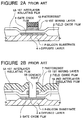
- FIG. 1D there is shown a conventional wiring and contact structure.
- a conventional method for forming the conventional wiring and contact structure will be described with reference to Figures 1A to 1D illustrating a process of the conventional method.
- a field oxide film 2 is formed on a p-type silicon substrate 1 by means of a conventional LOCOS (local oxidation of silicon) process, and after a gate oxide film 3 is formed on the substrate, an n-type diffused layer 4 is formed by ion-implanting for example arsenic.
- LOCOS local oxidation of silicon
- a silicon oxide film is deposited by for example a CVD (chemical vapor deposition) process so as to form a first interlayer insulating film 5A covering the field oxide film 2 and the gate oxide film 3, and then, for example, a tungsten silicide is deposited as a first wiring layer forming material.
- a photoresist 12 having a predetermined pattern is formed, and an etching is performed using the photoresist 12 as a mask, so as to form a first wiring layer 10. The photoresist 12 is removed.
- a silicon oxide film is deposited by for example the CVD process so as to form a second interlayer insulating film 18 covering the first wiring layer 10, the field oxide film 2 and the gate oxide film 3.
- a photoresist 7 having a predetermined pattern is formed, and the second and first interlayer insulating films 18 and 5A are selectively etched using the photoresist 7 as a mask, so as to form a contact hole 5B on the n-type diffused layer 4.
- a polysilicon film is deposited as a second wiring layer forming material filling the contact hole and covering the second interlayer insulating film 18. Then, a photoresist 19 having a predetermined pattern is formed, and the polysilicon film is etched using the photoresist 19 as a mask, so as to form a second wiring layer 14 electrically connected through the contact hole 5B on the n-type diffused layer 4.
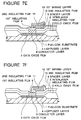
- JP-A-63-299142 shows one example of the improved wiring and contact structures.
- Figure 2E there is shown a sectional view of the improved wiring and contact structure proposed by JP-A-63-299142.
- Figures 2A to 2E are sectional views illustrating the process for manufacturing the improved wiring and contact structure.
- a field oxide film 2 is formed on a p-type silicon substrate 1 by means of a conventional LOCOS process, and then, a gate oxide film 3 is formed on the substrate. Furthermore, an n-type diffused layer 4 is formed by ion-implanting for example arsenic.
- a silicon oxide film is deposited by for example a CVD process so as to form a first interlayer insulating film 5A covering the field oxide film 2 and the gate oxide film 3, and then, for example, a tungsten silicide is deposited as a first wiring layer forming material. Furthermore, a photoresist 12 having a predetermined pattern is formed, and the silicide is patterned using the photoresist 12 as a mask, so as to form a first wiring layer 10. The photoresist 12 is removed.
- a silicon oxide film is deposited by for example the CVD process so as to form a second interlayer insulating film 18 covering the first wiring layer 10, the field oxide film 2 and the gate oxide film 3.
- a photoresist 7 having a predetermined pattern is formed, and the second interlayer insulating film 18, the first wiring layer 10, the first interlayer insulating film 5A and the gate oxide film 3 are selectively etched using the photoresist 7 as a mask, so as to form a contact hole 5B which causes a surface of the n-type diffused layer 4 to expose.
- a silicon oxide film is deposited by for example the CVD process so as to form an insulating film 20, and an anisotropic etching is formed to cause the insulating film 20 to remain only on a side surface of the contact hole 5B, as shown in Figure 2D.
- a polysilicon film is deposited as a second wiring layer forming material filling the contact hole and covering the second interlayer insulating film 18, and then, a photoresist 19 having a predetermined pattern is formed. Furthermore, the polysilicon film is etched using the photoresist 19 as a mask, so as to form a second wiring layer 14 electrically connected through the contact hole 5B on the n-type diffused layer 4 but electrically insulated from the first wiring layer 10.
- the photoresist process for forming the pad must be newly added, and since there is required an alignment margin between the first wiring layer 10 and the contact hole connecting the second wiring layer 14 to the pad, it is not satisfactory in structure to realize a high integration density.
- Another object of the present invention is to provide a wiring and contact structure having a reduced contact resistance and capable of realizing microminiaturization, and a method for forming the wiring and contact structure without an additional photoresist mask process.
- a semiconductor device comprising a semiconductor substrate, a conducting layer formed in the semiconductor substrate, an interlayer insulating layer formed above the conducting layer, a contact hole formed in the interlayer insulating layer to expose a surface of the conducting layer, a conductive material layer filled in the contact hole, a first wiring layer formed to have a part overlapping a part of the conductive material layer, a first insulating film formed between the conductive material layer and the first wiring layer, a second insulating film formed on an upper surface of the first wiring layer having the same pattern as that of the first wiring layer, a side wall insulating film formed on a side surface of the first wiring layer, and a second wiring layer formed in contact with the conductive material layer but insulated from the first wiring layer by the second insulating film and the side wall insulating film.
- a method for manufacturing a semiconductor device comprising: the step of depositing an interlayer insulating film on a semiconductor substrate; the step of selectively etching the interlayer insulating film so as to form a contact hole in which a surface of an underlying conducting layer is exposed; the step of forming a conductive material layer filling the contact hole; the step of forming a first insulating film covering an exposed surface of the conductive material layer; the step of depositing a first wiring material layer and a second insulating film in the named order, and patterning a stacked layer of the first wiring material layer and the second insulating film, so as to form a first wiring layer which has its part overlapping a part of the conductive material layer and which has its upper surface covered with the second insulating film; the step of depositing a third insulating film on a whole surface and etching back the deposited third insulating film so as to form a side wall insulating film covering a side surface of the first
- FIG. 4 there is shown a diagrammatic sectional view illustrating a first embodiment of the wring and contact structure in accordance with the present invention.
- the first embodiment includes a p-type silicon substrate 1 having an n-type diffused layer 4 formed in a surface region defined by a field oxide film 2 also formed on the substrate 1.
- a contact hole is formed to pass through an gate oxide film 3 and an interlayer insulating film 5 which are formed on the n-type diffused layer 4 in the named order.
- the contact hole is filled with a conductive material layer 8, which projects upward from an upper surface of the interlayer insulating film 5.
- first wiring layer 10 On the conductive material layer 8, there is formed a first wiring layer 10 having its part covering a part of the conductive material layer 8 through a first insulating layer 9. An an upper surface of the first wiring layer 10 is covered with a second insulating layer 11 having the same pattern as that of the first wiring layer 10, and a side surface of the first wiring layer 10 is covered with a third insulating film 13 formed as a side wall. On the conductive material layer 8 and the first wiring layer 10, there is formed a second wiring layer 14 which is in contact with the conductive material layer 8 but which is insulated from the first wiring layer 10 by the second insulating layer 11 and the third insulating film 13.
- the first wiring layer in such a manner that a part of the first wiring layer overlaps the contact portion, and (2) it is no longer necessary to consider an alignment margin between the contact hole and the first wiring layer and an alignment margin between the first wiring layer and the second wiring layer. Therefore, it is possible to further microminiaturize the connection structure in comparison with the prior art structures mentioned hereinbefore.
- the second wiring layer since the second wiring layer is in contact with not only the upper surface but also the side surface of the conductive material layer, the contact resistance can be maintained small.
- a field oxide film 2 having a thickness of about 4000 ⁇ is formed by means of a conventional LOCOS process, and then, a gate oxide film 3 having a thickness of about 150 ⁇ is formed by a thermal oxidation. Furthermore, an n-type diffused layer 4 is formed by ion-implanting for example arsenic under an energy of 50 KeV and a dose of 1.0 ⁇ 1015cm ⁇ 2.
- a silicon oxide film having a thickness of about 3000 ⁇ is deposited by for example a CVD process so as to form an interlayer insulating film 5, and then, a silicon nitride film having a thickness of about 2000 ⁇ , having a film property different from that of the interlayer insulating film 5, is deposited by for example a CVD process so as to form a spacer layer 6.
- a photoresist 7 having a predetermined pattern is formed, and the spacer layer 6, the interlayer insulating film 5 and the gate oxide film 3 are selectively etched using the photoresist 7 as a mask, so as to form a contact hole 5B in which a surface of the n-type diffused layer 4 is exposed, as shown in Figure 5A.
- a polysilicon film having a thickness of about 3000 ⁇ is grown, and the grown polysilicon film is etched back by an anisotropic etching so as to form a conductive material layer 8 filling the contact hole 5B.
- the spacer layer (silicon nitride) 6 is removed by an etching. Furthermore, as shown in Figure 5D, a surface of a portion of the polysilicon film (conductive material layer 8) projecting from the interlayer insulating film 5 is thermally oxidized to form a silicon oxide film having a thickness of about 500 ⁇ , as a first insulating film 9.
- a tungsten silicide film having a thickness of about 2000 ⁇ is deposited as a first wiring material layer 10A by a sputtering, and furthermore, a silicon nitride film having a thickness of about 1000 ⁇ is grown as a second insulating film 11 by the CVD process. Thereafter, a photoresist mask 12 is formed on a first wiring layer forming position by a photolithography.
- an anisotropic etching is performed to pattern the second insulating film 11 and the first wiring material layer 10A, so that a first wiring layer 10 is formed. Then, the photoresist mask 12 is removed.
- a silicon nitride film having a thickness of about 800 ⁇ is grown as a third insulating film 13 by the CVD process, and succeedingly, as shown in Figure 5H, an anisotropic etching is performed for the third insulating film 13 so that the third insulating film 13 remains as a side wall on only a side surface of the first wiring layer 10.
- an exposed first insulting film 9 is removed by an isotopic etching.
- a polysilicon film having a thickness of about 3000 ⁇ is grown, and the grown polysilicon film is patterned so as to form a second wiring layer 14.
- the required photoresist mask process includes only three steps, namely, the contact hole forming step, the first wiring layer patterning step and the second wiring layer patterning step. Accordingly, the number of required photoresist mask steps is the same as that required in the conventional example shown in Figure 1.
- the second embodiment is characterized in that the spacer layer 6 is left under the first wiring layer 10, and therefore, since the first wiring layer can be formed on a planarized surface, even if the first wiring layer is thin in film thickness, it is possible to reduce possibility that the first wiring layer becomes open-circuited at a step portion.
- a field oxide film 2 having a thickness of about 4000 ⁇ is formed on a p-type silicon substrate 1 by means of a conventional LOCOS process, and then, a gate oxide film 3 having a thickness of about 150 ⁇ is formed by a thermal oxidation. Furthermore, an n-type diffused layer 4 is formed by ion-implanting for example arsenic under an energy of 50 KeV and a dose of 1.0 ⁇ 1015cm ⁇ 2.
- a silicon oxide film having a thickness of about 3000 ⁇ is deposited by for example a CVD process so as to form an interlayer insulating film 5, and then, a silicon nitride film having a thickness of about 2000 ⁇ and having a film property different from that of the interlayer insulating film 5, is deposited by for example a CVD process so as to form a spacer layer 6.
- a photoresist 7 having a predetermined pattern is formed, and the spacer layer 6, the interlayer insulating film 5 and the gate oxide film 3 are selectively etched using the photoresist 7 as a mask, so as to form a contact hole 5B in which a surface of the n-type diffused layer 4 is exposed, as shown in Figure 7A.
- a polysilicon film having a thickness of about 3000 ⁇ is grown, and the grown polysilicon film is etched back by an anisotropic etching so as to form a conductive material layer 8 filling the contact hole 5B.
- a thermal oxidation is performed to form a silicon oxide film having a thickness of about 500 ⁇ , on an exposed surface of the polysilicon film (conductive material layer 8), as a first insulating film 9.
- a tungsten silicide film having a thickness of about 2000 ⁇ is deposited as a first wiring material layer by a sputtering, and furthermore, a silicon nitride film having a thickness of about 2000 ⁇ is grown as a second insulating film 11 by the CVD process.
- a photoresist mask 12 is formed on a first wiring layer forming position by a photolithography, and an anisotropic etching is performed to pattern the second insulating film 11 and the first wiring material layer, so that a first wiring layer 10 is formed. Then, the photoresist mask 12 is removed.
- a silicon oxide film having a thickness of about 1000 ⁇ is grown as a third insulating film 13 by the CVD process, and succeedingly, as shown in Figure 7F, an anisotropic etching is performed so that the third insulating film 13 and the first insulating film 9 are removed on a planar portion, and on the other hand, a portion of the third insulating film 13 remains as a side wall on only a side surface of the first wiring layer 10. In this process, the film thickness of the second insulting film 11 is considerably reduced.
- an exposed spacer layer 6 is removed by etching using the first, second and third insulating films as a mask
- a polysilicon film having a thickness of about 3000 ⁇ is grown, and the grown polysilicon film is patterned so as to form a second wiring layer 14.
- Figures 8A to 8D are diagrammatic sectional views illustrating a processing for forming a third embodiment of the wring and contact structure in accordance with the present invention.
- elements similar to those shown in Figures 5A to 5J are given the same Reference Numerals.
- a field oxide film 2 and a gate oxide film 3 are formed in the named order, and an n-type diffused layer 4 is formed in a surface of the substrate.
- an interlayer insulating film 5 composed of a silicon oxide film having a thickness of about 3000 ⁇
- a spacer layer 6 composed of a silicon nitride film having a thickness of about 2000 ⁇ , are deposited in the named order.
- the spacer layer 6, the interlayer insulating film 5 and the gate oxide film 3 are selectively etched so as to form a contact hole in which a surface of the n-type diffused layer 4 is exposed.
- a tungsten (W) is selectively grown within the contact hole so as to form a conductive material layer 8 as shown in Figure 8A.
- a silicon nitride film having a thickness of about 1000 ⁇ is grown by the CVD process so as to form a first insulating film 9, as shown in Figure 8B.
- a tungsten silicide film having a thickness of about 2000 ⁇ is deposited as a first wiring material layer by a sputtering, and furthermore, a silicon oxide film having a thickness of about 1000 ⁇ is grown as a second insulating film 11 by the CVD process. Thereafter, these deposited films are patterned by a photolithography, so that a first wiring layer 10 having the second insulating film 11 deposited thereon is formed.
- a silicon oxide film having a thickness of about 1000 ⁇ is grown as a third insulating film 13 by the CVD process, and succeedingly, an anisotropic etching is performed for the third insulating film 13 so that a portion of the third insulating film 13 remains as a side wall on only a side surface of the first wiring layer 10, as shown in Figure 8C.
- an exposed first insulting film 9 is etched using the second and third insulating films as a mask, and furthermore, an aluminum layer is deposited and patterned so as to form a second wiring layer 14.
- an aluminum layer is deposited and patterned so as to form a second wiring layer 14.
- FIG. 9 there is shown a diagrammatic sectional view illustrating a fourth embodiment of the wring and contact structure in accordance with the present invention.
- elements similar to those shown in Figure 4 are given the same Reference Numerals, and explanation thereof will be omitted for simplification of description.
- the fourth embodiment is characterized in that a capacitor lower electrode 15 composed of polysilicon is formed in place of the second wiring layer 14, and furthermore, a capacitor dielectric film 16 is formed on the capacitor lower electrode 15 and a capacitor upper electrode 17 is formed on the capacitor dielectric film 16.
- a capacitor is formed. Therefore, it could be understood that the present invention can be applied to a memory cell of a DRAM (dynamic random access memory).
- DRAM dynamic random access memory
- the contact is formed for the n-type diffused layer, but the present invention is not limited to these embodiments.
- the wiring and contact structure of the present invention can be equally applied to a p-type diffused layer and other wiring layer.
- the first and second wiring layers may be connected to other n-type diffused layers, or other wiring conductors.
- the present invention can be applied to not only a MOS type of semiconductor device but also other types of semiconductor device.
Landscapes
- Internal Circuitry In Semiconductor Integrated Circuit Devices (AREA)
- Semiconductor Memories (AREA)
- Semiconductor Integrated Circuits (AREA)
Applications Claiming Priority (3)
| Application Number | Priority Date | Filing Date | Title |
|---|---|---|---|
| JP20284394 | 1994-08-04 | ||
| JP6202843A JP2616706B2 (ja) | 1994-08-04 | 1994-08-04 | 半導体装置およびその製造方法 |
| JP202843/94 | 1994-08-04 |
Publications (3)
| Publication Number | Publication Date |
|---|---|
| EP0696060A2 true EP0696060A2 (de) | 1996-02-07 |
| EP0696060A3 EP0696060A3 (de) | 1997-07-09 |
| EP0696060B1 EP0696060B1 (de) | 2001-11-07 |
Family
ID=16464118
Family Applications (1)
| Application Number | Title | Priority Date | Filing Date |
|---|---|---|---|
| EP95112334A Expired - Lifetime EP0696060B1 (de) | 1994-08-04 | 1995-08-04 | Herstellungsverfahren für eine Verdrahtung und eine Kontaktstruktur einer Halbleitervorrichtung |
Country Status (5)
| Country | Link |
|---|---|
| US (2) | US5581124A (de) |
| EP (1) | EP0696060B1 (de) |
| JP (1) | JP2616706B2 (de) |
| KR (1) | KR0174069B1 (de) |
| DE (1) | DE69523682T9 (de) |
Cited By (1)
| Publication number | Priority date | Publication date | Assignee | Title |
|---|---|---|---|---|
| EP1058304A1 (de) * | 1999-05-31 | 2000-12-06 | STMicroelectronics S.r.l. | Verfahren zur Selbstausrichtung überlappender Leiterbahnen in integrierten elektronischen Schaltungen |
Families Citing this family (4)
| Publication number | Priority date | Publication date | Assignee | Title |
|---|---|---|---|---|
| JP3602896B2 (ja) * | 1995-09-29 | 2004-12-15 | アルプス電気株式会社 | シート状スイッチ |
| US5973385A (en) * | 1996-10-24 | 1999-10-26 | International Business Machines Corporation | Method for suppressing pattern distortion associated with BPSG reflow and integrated circuit chip formed thereby |
| KR100745057B1 (ko) * | 2001-06-27 | 2007-08-01 | 주식회사 하이닉스반도체 | 반도체 소자의 제조 방법 |
| JP2007273871A (ja) * | 2006-03-31 | 2007-10-18 | Toshiba Corp | 設計データ作成方法、設計データ作成プログラム、及び半導体装置の製造方法 |
Citations (1)
| Publication number | Priority date | Publication date | Assignee | Title |
|---|---|---|---|---|
| JPS63299142A (ja) | 1987-05-28 | 1988-12-06 | Nec Corp | 多層配線構造を有する半導体装置の製造方法 |
Family Cites Families (11)
| Publication number | Priority date | Publication date | Assignee | Title |
|---|---|---|---|---|
| US4409722A (en) * | 1980-08-29 | 1983-10-18 | International Business Machines Corporation | Borderless diffusion contact process and structure |
| JPS57120295A (en) * | 1981-01-17 | 1982-07-27 | Mitsubishi Electric Corp | Semiconductor memory device |
| US4617193A (en) * | 1983-06-16 | 1986-10-14 | Digital Equipment Corporation | Planar interconnect for integrated circuits |
| JPH0618257B2 (ja) * | 1984-04-28 | 1994-03-09 | 富士通株式会社 | 半導体記憶装置の製造方法 |
| US4948755A (en) * | 1987-10-08 | 1990-08-14 | Standard Microsystems Corporation | Method of manufacturing self-aligned conformal metallization of semiconductor wafer by selective metal deposition |
| JPH02211651A (ja) * | 1989-02-10 | 1990-08-22 | Mitsubishi Electric Corp | 半導体装置およびその製造方法 |
| US5172202A (en) * | 1989-05-31 | 1992-12-15 | Nec Corporation | Semiconductor memory cell having high density structure |
| JPH04226054A (ja) * | 1990-03-02 | 1992-08-14 | Toshiba Corp | 多層配線構造を有する半導体装置及びその製造方法 |
| US5061646A (en) * | 1990-06-29 | 1991-10-29 | Motorola, Inc. | Method for forming a self-aligned bipolar transistor |
| JPH0555466A (ja) * | 1991-01-23 | 1993-03-05 | Matsushita Electric Ind Co Ltd | 半導体記憶装置およびその製造方法 |
| JP2906807B2 (ja) * | 1992-03-04 | 1999-06-21 | 日本電気株式会社 | 半導体メモリセルとその製造方法 |
-
1994
- 1994-08-04 JP JP6202843A patent/JP2616706B2/ja not_active Expired - Fee Related
-
1995
- 1995-08-03 KR KR1019950023919A patent/KR0174069B1/ko not_active Expired - Fee Related
- 1995-08-04 EP EP95112334A patent/EP0696060B1/de not_active Expired - Lifetime
- 1995-08-04 US US08/511,301 patent/US5581124A/en not_active Expired - Fee Related
- 1995-08-04 DE DE69523682T patent/DE69523682T9/de not_active Expired - Fee Related
- 1995-12-22 US US08/577,860 patent/US5536682A/en not_active Expired - Fee Related
Patent Citations (1)
| Publication number | Priority date | Publication date | Assignee | Title |
|---|---|---|---|---|
| JPS63299142A (ja) | 1987-05-28 | 1988-12-06 | Nec Corp | 多層配線構造を有する半導体装置の製造方法 |
Cited By (2)
| Publication number | Priority date | Publication date | Assignee | Title |
|---|---|---|---|---|
| EP1058304A1 (de) * | 1999-05-31 | 2000-12-06 | STMicroelectronics S.r.l. | Verfahren zur Selbstausrichtung überlappender Leiterbahnen in integrierten elektronischen Schaltungen |
| US6350671B1 (en) | 1999-05-31 | 2002-02-26 | Stmicroelectronics S.R.L. | Method for autoaligning overlapped lines of a conductive material in integrated electronic circuits |
Also Published As
| Publication number | Publication date |
|---|---|
| DE69523682T2 (de) | 2002-08-01 |
| KR0174069B1 (ko) | 1999-04-01 |
| DE69523682T9 (de) | 2004-09-09 |
| JPH0851146A (ja) | 1996-02-20 |
| US5536682A (en) | 1996-07-16 |
| EP0696060A3 (de) | 1997-07-09 |
| DE69523682D1 (de) | 2001-12-13 |
| US5581124A (en) | 1996-12-03 |
| JP2616706B2 (ja) | 1997-06-04 |
| EP0696060B1 (de) | 2001-11-07 |
| KR960009021A (ko) | 1996-03-22 |
Similar Documents
| Publication | Publication Date | Title |
|---|---|---|
| US6251790B1 (en) | Method for fabricating contacts in a semiconductor device | |
| US20020024093A1 (en) | Semiconductor device with self-aligned contact structure employing dual spacers and method of manufacturing the same | |
| JPH0917978A (ja) | 高集積dram素子及びその製造方法 | |
| JP3022744B2 (ja) | 半導体装置及びその製造方法 | |
| US6197670B1 (en) | Method for forming self-aligned contact | |
| US6511879B1 (en) | Interconnect line selectively isolated from an underlying contact plug | |
| JP2578577B2 (ja) | コンタクトホール形成方法 | |
| JP3757143B2 (ja) | 半導体装置の製造方法及び半導体装置 | |
| KR100277377B1 (ko) | 콘택트홀/스루홀의형성방법 | |
| US5827770A (en) | Method of making a semiconductor device having improved contacts to a thin conductive layer | |
| US5554864A (en) | Semiconductor device having improved coverage with increased wiring layers | |
| US6953744B2 (en) | Methods of fabricating integrated circuit devices providing improved short prevention | |
| KR100273987B1 (ko) | 디램 장치 및 제조 방법 | |
| US20010024854A1 (en) | Semiconductor storage device and method of fabricating thereof | |
| CN118943128A (zh) | 金属-绝缘体-金属电容及其形成方法 | |
| KR100294755B1 (ko) | 반도체장치및그제조방법 | |
| KR20030076246A (ko) | 아날로그 커패시터를 갖는 반도체 소자 및 그 제조방법 | |
| US6284619B1 (en) | Integration scheme for multilevel metallization structures | |
| EP0827195A1 (de) | Verbesserungen an Halbleiteranordnungen | |
| US5536682A (en) | Method for manufacturing a semiconductor device | |
| US20040018754A1 (en) | Conductive contact structure and process | |
| JP3120750B2 (ja) | 半導体装置およびその製造方法 | |
| JP2914303B2 (ja) | 半導体装置の製造方法 | |
| JP3288910B2 (ja) | 半導体装置の製造方法 | |
| KR20000026376A (ko) | 다층 배선 형성을 위한 다마신 방법 |
Legal Events
| Date | Code | Title | Description |
|---|---|---|---|
| PUAI | Public reference made under article 153(3) epc to a published international application that has entered the european phase |
Free format text: ORIGINAL CODE: 0009012 |
|
| AK | Designated contracting states |
Kind code of ref document: A2 Designated state(s): DE FR GB |
|
| PUAL | Search report despatched |
Free format text: ORIGINAL CODE: 0009013 |
|
| AK | Designated contracting states |
Kind code of ref document: A3 Designated state(s): DE FR GB |
|
| 17P | Request for examination filed |
Effective date: 19970530 |
|
| 17Q | First examination report despatched |
Effective date: 19990616 |
|
| GRAG | Despatch of communication of intention to grant |
Free format text: ORIGINAL CODE: EPIDOS AGRA |
|
| GRAG | Despatch of communication of intention to grant |
Free format text: ORIGINAL CODE: EPIDOS AGRA |
|
| GRAH | Despatch of communication of intention to grant a patent |
Free format text: ORIGINAL CODE: EPIDOS IGRA |
|
| GRAH | Despatch of communication of intention to grant a patent |
Free format text: ORIGINAL CODE: EPIDOS IGRA |
|
| GRAH | Despatch of communication of intention to grant a patent |
Free format text: ORIGINAL CODE: EPIDOS IGRA |
|
| GRAA | (expected) grant |
Free format text: ORIGINAL CODE: 0009210 |
|
| AK | Designated contracting states |
Kind code of ref document: B1 Designated state(s): DE FR GB |
|
| REF | Corresponds to: |
Ref document number: 69523682 Country of ref document: DE Date of ref document: 20011213 |
|
| REG | Reference to a national code |
Ref country code: GB Ref legal event code: IF02 |
|
| ET | Fr: translation filed | ||
| PLBE | No opposition filed within time limit |
Free format text: ORIGINAL CODE: 0009261 |
|
| STAA | Information on the status of an ep patent application or granted ep patent |
Free format text: STATUS: NO OPPOSITION FILED WITHIN TIME LIMIT |
|
| 26N | No opposition filed | ||
| REG | Reference to a national code |
Ref country code: GB Ref legal event code: 732E |
|
| PGFP | Annual fee paid to national office [announced via postgrant information from national office to epo] |
Ref country code: GB Payment date: 20030730 Year of fee payment: 9 |
|
| PGFP | Annual fee paid to national office [announced via postgrant information from national office to epo] |
Ref country code: FR Payment date: 20030808 Year of fee payment: 9 |
|
| PGFP | Annual fee paid to national office [announced via postgrant information from national office to epo] |
Ref country code: DE Payment date: 20030814 Year of fee payment: 9 |
|
| REG | Reference to a national code |
Ref country code: FR Ref legal event code: TP |
|
| PG25 | Lapsed in a contracting state [announced via postgrant information from national office to epo] |
Ref country code: GB Free format text: LAPSE BECAUSE OF NON-PAYMENT OF DUE FEES Effective date: 20040804 |
|
| PG25 | Lapsed in a contracting state [announced via postgrant information from national office to epo] |
Ref country code: DE Free format text: LAPSE BECAUSE OF NON-PAYMENT OF DUE FEES Effective date: 20050301 |
|
| GBPC | Gb: european patent ceased through non-payment of renewal fee |
Effective date: 20040804 |
|
| PG25 | Lapsed in a contracting state [announced via postgrant information from national office to epo] |
Ref country code: FR Free format text: LAPSE BECAUSE OF NON-PAYMENT OF DUE FEES Effective date: 20050429 |
|
| REG | Reference to a national code |
Ref country code: FR Ref legal event code: ST |