EP0696056A2 - Doppelmasken, hermetische Passivierungsstruktur - Google Patents
Doppelmasken, hermetische Passivierungsstruktur Download PDFInfo
- Publication number
- EP0696056A2 EP0696056A2 EP95304787A EP95304787A EP0696056A2 EP 0696056 A2 EP0696056 A2 EP 0696056A2 EP 95304787 A EP95304787 A EP 95304787A EP 95304787 A EP95304787 A EP 95304787A EP 0696056 A2 EP0696056 A2 EP 0696056A2
- Authority
- EP
- European Patent Office
- Prior art keywords
- passivation layer
- forming
- integrated circuit
- portions
- pads
- Prior art date
- Legal status (The legal status is an assumption and is not a legal conclusion. Google has not performed a legal analysis and makes no representation as to the accuracy of the status listed.)
- Granted
Links
Images

Classifications
-
- H10P74/23—
-
- H10W20/494—
-
- H10W74/137—
-
- Y—GENERAL TAGGING OF NEW TECHNOLOGICAL DEVELOPMENTS; GENERAL TAGGING OF CROSS-SECTIONAL TECHNOLOGIES SPANNING OVER SEVERAL SECTIONS OF THE IPC; TECHNICAL SUBJECTS COVERED BY FORMER USPC CROSS-REFERENCE ART COLLECTIONS [XRACs] AND DIGESTS
- Y10—TECHNICAL SUBJECTS COVERED BY FORMER USPC
- Y10S—TECHNICAL SUBJECTS COVERED BY FORMER USPC CROSS-REFERENCE ART COLLECTIONS [XRACs] AND DIGESTS
- Y10S438/00—Semiconductor device manufacturing: process
- Y10S438/958—Passivation layer
Definitions
- This invention relates in general to passivation structures, and more particularly to double mask hermetic passivation structures.
- Modern memory integrated circuits particularly read/write circuits, such as static random access memories (SRAMs) and dynamic random access memories (DRAMs), are being quite large in physical size and in the density of memory locations therein.
- SRAMs static random access memories
- DRAMs dynamic random access memories
- SRAMs static random access memories
- DRAMs dynamic random access memories
- Substitution of one of the spare rows or columns is conventionally accomplished by the opening of linking structures, such as fusible links, in decoder circuitry, so that access is made to the spare row or column upon receipt of the address for the defective row or column in the primary memory array.
- linking structures such as fusible links
- Conventional fuses include polysilicon fuses, which can be opened by a laser beam. Avalanche-type fuses and anti-fuses may also be used to provide the proper connections.
- a third alternative is to eliminate the masking of the integrated circuit with the first passivation layer, such that the entire surface of the integrated circuit is exposed during the test for identifying defective rows and columns. Using this method, the testing and laser disconnect steps are performed without the benefit of a protective film covering the majority of the integrated circuit, thereby subjecting the integrated circuit to contamination during this phase.
- a passivation structure is created over an integrated circuit by forming a first passivation layer over the integrated circuit and removing portions of the first passivation layer to expose pads and fusible links of the integrated circuit. After testing the integrated circuit and disconnecting one or more of the fusible links, a second passivation structure is formed over the surface of the integrated circuit and a protective overcoat is formed over the second passivation layer. Portions of the protective overcoats surrounding the pads are removed, thereby exposing portions of the second passivation layer. The exposed portions of the second passivation layer are removed using the protective overcoat as a mask.
- the present invention provides significant advantages over the prior art. Importantly, the masking levels associated with the passivation structure are reduced over the prior art, without affecting the reliability of the devices.
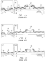
- FIGUREs 1-4 of the drawings like numerals being used for like and corresponding parts of the various drawings.
- Figures 1a-e illustrate five stages of the formation of a prior art passivation structure which uses two passivation layers, one formed prior to testing and one formed after laser repair, and a protective overcoat.
- This prior art structure requires three masking levels to form the passivation structure.
- steps of forming the devices on the integrated circuit are not shown.
- Devices (shown generally at block 11) are formed at the surface of substrate 12 using well-known techniques.
- One or more interconnect layers are formed to connect the devices as desired.
- a metal pad 10 (generally part of one of the interconnect layers 13) is provided as a connection to the circuitry formed on the surface of the substrate 12.
- a polysilicon gate 14 is formed above the substrate 12 for use as a fusible link. Although not shown to scale for illustration purposes, the polysilicon gate 14 is typically formed at a level below pad 10.
- a first passivation layer 16 is formed over the surface of the wafer.
- the first passivation layer 16 is etched to provide an opening 18 to the polysilicon gate 14 and an opening 20 over the pad 10.
- a dielectric layer (not shown) having a thickness of 2000-8000 Angstroms is left over the polysilicon gate 14 to assist with the laser repair step described below in connection with Figure 1c.
- the first passivation layer 16 may be formed, for example, by deposit of a dielectric film followed by pattern and etching to form the openings 18 and 20. The pattern and etch is the first masking step used in this process to form the passivation structure. While Figure 1a shows a single gate 14 and pad 10, it should be noted that there are a plurality of gates 14 and pads 10 formed over the integrated circuit.
- the integrated circuit may be tested by probing the circuit at the pads 10. This test will determine which rows and/or columns should be disconnected to form a defect-free circuit. Once the proper rows and/or columns are detected, the associated polysilicon gates 14 are vaporized using a laser. Figure 1c shows a disconnected portion 22 in the polysilicon gate 14.
- a second passivation layer 24 is formed over the entire surface of the wafer, thereby sealing the disconnected portion 22 in the polysilicon gate 14. This layer forms a hermetic seal over all such disconnected portions 22.
- the second passivation layer 24 is etched to form a window 26 over the pad 10.
- the second passivation layer 24 could comprise, for example, a deposited silicon nitride layer.
- the silicon nitride layer could be etched using a plasma etch after a masking step to expose the pads 10. This is the second masking step used in the verification of the passivation structure.
- Figure 1e illustrates a cross-sectional sideview of the passivation structure after a fifth stage wherein a protection overcoat (also referred to as a "die coat") 30 is formed over the entire wafer.
- the protective overcoat is patterned and etched to expose the area surrounding the pads 10. This step comprises the third masking step used in the process.
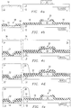
- Figure 2 illustrates a prior art structure made in the process similar to that shown in Figures 1a-e, except the step shown in Figure 1d is eliminated. Consequently, the second passivation layer, which in the structure of Figures 1a-1e covers the disconnected portions 22 of the polysilicon gate 14 after the laser repair step, is eliminated from the structure and the protective overcoat 30 fills the disconnected portions 22. While only two masking levels are used in this process, one masking level to form the openings 18 and 20 in the first passivation layer 16 and one to pattern the protective overcoat 30, the disconnected portions 22 are not hermetically sealed. Consequently, the openings formed by laser repair in the polysilicon gate 14 are points of possible moisture entry.
- PSG polysilicon glass
- Figure 3 illustrates a third prior art embodiment of forming a passivation structure in which the number of masking levels is reduced by testing the integrated circuit without the benefit of a protective layer (i.e., passivation layer 16) to protect the integrated circuit during testing.
- a protective layer i.e., passivation layer 16
- yield loss can occur from a number of sources.
- Figures 4a-e illustrate cross-sectional sideviews of a passivation structure after respective stages of processing.
- Figure 4a shows an initial stage wherein the polysilicon fuse 14 and pad 10 have been formed over substrate 12.
- the pads 10 are connected to the devices previously formed at the face of substrate 12.
- Various devices are coupled through one or more interconnect layers, typically using metal layers formed over the devices (and separated therefrom by dielectric layers) and using common bitlines and wordlines formed as part of the devices.
- a first passivation layer 16 is formed over the wafer and is etched to form the openings 18 and 20, as shown in connection with Figure 1b.
- the first passivation layer 16 may comprise, for example, a dielectric film of approximately 2k angstroms to 15k angstroms.
- the material for the passivation layer may be a silicon oxide, PSG, or silicon oxynitride (Si x O y N z ).
- the devices on the wafer are tested to identify defective elements using well-known techniques. Thereafter, laser repair is performed by forming disconnected regions 22 in the polysilicon gate 14, as shown in connection with Figure 1c.
- a second dielectric film 32 of approximately 200-5,000 Angstroms is deposited over the surface of the wafer.
- This second passivation layer 32 may comprise, for example, silicon oxide, PSG, silicon oxynitride, or silicon nitride.
- the second passivation layer should be a different material than the first passivation layer 16, since a selective etch will be used in a later step.
- the same material could be used for both passivation layers, and a timed etch could remove the second passivation layer 32, while leaving a sufficient thickness of the first passivation layer 16.
- the second passivation layer 32 is not patterned and masked. Instead, the protective overcoat, for example, a polyimide, 34 is formed over the entire wafer. A mask 36 is patterned over the protective overcoat layer 34 using photolithographic techniques.
- the protective overcoat for example, a polyimide
- the protective overcoat 34 is etched using an organic or other suitable etch which is selective to the second passivation layer 32. The etch removes portions of the protective overcoat surrounding the pads 10.
- the remaining portions of the protective overcoat 34 are used as a mask for the second passivation layer 32.
- a plasma etch which is selective to the protective overcoat 34 and the first passivation layer 16
- the portions of the second passivation layer 32 surrounding the pads 10 are removed, thereby exposing the opening 20 to the pad.
- the leads can be attached to the pads 10 and the integrated circuits can be encapsulated for packaging.
- a passivation structure is shown with complete hermetic sealing by using two passivation layers and a protective overcoat layer, performed using only two masking steps. Consequently, the cost of producing the passivation structure is reduced without affecting the reliability of the underlying devices.
Landscapes
- Design And Manufacture Of Integrated Circuits (AREA)
Applications Claiming Priority (2)
| Application Number | Priority Date | Filing Date | Title |
|---|---|---|---|
| US28282994A | 1994-07-29 | 1994-07-29 | |
| US282829 | 1994-07-29 |
Publications (3)
| Publication Number | Publication Date |
|---|---|
| EP0696056A2 true EP0696056A2 (de) | 1996-02-07 |
| EP0696056A3 EP0696056A3 (de) | 1996-09-11 |
| EP0696056B1 EP0696056B1 (de) | 2000-01-19 |
Family
ID=23083308
Family Applications (1)
| Application Number | Title | Priority Date | Filing Date |
|---|---|---|---|
| EP95304787A Expired - Lifetime EP0696056B1 (de) | 1994-07-29 | 1995-07-10 | Verfahren zum Testen und Reparieren eines integrierten Schaltkreises und zum Herstellen einer Passivierungsstruktur |
Country Status (3)
| Country | Link |
|---|---|
| US (2) | US5698456A (de) |
| EP (1) | EP0696056B1 (de) |
| DE (1) | DE69514588T2 (de) |
Families Citing this family (14)
| Publication number | Priority date | Publication date | Assignee | Title |
|---|---|---|---|---|
| US6046101A (en) * | 1997-12-31 | 2000-04-04 | Intel Corporation | Passivation technology combining improved adhesion in passivation and a scribe street without passivation |
| US6875681B1 (en) * | 1997-12-31 | 2005-04-05 | Intel Corporation | Wafer passivation structure and method of fabrication |
| DE19800566A1 (de) * | 1998-01-09 | 1999-07-15 | Siemens Ag | Verfahren zum Herstellen eines Halbleiterbauelementes und ein derart hergestelltes Halbleiterbauelement |
| US6352940B1 (en) * | 1998-06-26 | 2002-03-05 | Intel Corporation | Semiconductor passivation deposition process for interfacial adhesion |
| US20070190751A1 (en) * | 1999-03-29 | 2007-08-16 | Marr Kenneth W | Semiconductor fuses and methods for fabricating and programming the same |
| US6352881B1 (en) | 1999-07-22 | 2002-03-05 | National Semiconductor Corporation | Method and apparatus for forming an underfill adhesive layer |
| US6368902B1 (en) | 2000-05-30 | 2002-04-09 | International Business Machines Corporation | Enhanced efuses by the local degradation of the fuse link |
| US7423337B1 (en) | 2002-08-19 | 2008-09-09 | National Semiconductor Corporation | Integrated circuit device package having a support coating for improved reliability during temperature cycling |
| US20040038458A1 (en) * | 2002-08-23 | 2004-02-26 | Marr Kenneth W. | Semiconductor fuses, semiconductor devices containing the same, and methods of making and using the same |
| US7301222B1 (en) | 2003-02-12 | 2007-11-27 | National Semiconductor Corporation | Apparatus for forming a pre-applied underfill adhesive layer for semiconductor wafer level chip-scale packages |
| US7282375B1 (en) * | 2004-04-14 | 2007-10-16 | National Semiconductor Corporation | Wafer level package design that facilitates trimming and testing |
| KR20060077536A (ko) * | 2004-12-30 | 2006-07-05 | 동부일렉트로닉스 주식회사 | 씨모스 이미지 센서 및 그의 제조방법 |
| EP1717863B1 (de) | 2005-04-28 | 2011-11-02 | Ixys Corporation | Leistungshalbleiteranordnung mit Passivierungsschichten |
| US20150255362A1 (en) | 2014-03-07 | 2015-09-10 | Infineon Technologies Ag | Semiconductor Device with a Passivation Layer and Method for Producing Thereof |
Citations (2)
| Publication number | Priority date | Publication date | Assignee | Title |
|---|---|---|---|---|
| US4573146A (en) | 1982-04-20 | 1986-02-25 | Mostek Corporation | Testing and evaluation of a semiconductor memory containing redundant memory elements |
| US5257229A (en) | 1992-01-31 | 1993-10-26 | Sgs-Thomson Microelectronics, Inc. | Column redundancy architecture for a read/write memory |
Family Cites Families (16)
| Publication number | Priority date | Publication date | Assignee | Title |
|---|---|---|---|---|
| JPS5889814A (ja) * | 1981-11-25 | 1983-05-28 | Toshiba Corp | 箔巻変圧器 |
| JPS59214239A (ja) * | 1983-05-16 | 1984-12-04 | Fujitsu Ltd | 半導体装置の製造方法 |
| JPS6065545A (ja) * | 1983-09-21 | 1985-04-15 | Hitachi Micro Comput Eng Ltd | 半導体装置の製造方法 |
| JPS6122650A (ja) * | 1984-07-11 | 1986-01-31 | Hitachi Ltd | 欠陥救済方法および装置 |
| US5017510A (en) * | 1987-06-01 | 1991-05-21 | Texas Instruments Incorporated | Method of making a scalable fuse link element |
| JPH0654774B2 (ja) * | 1987-11-30 | 1994-07-20 | 株式会社東芝 | 半導体装置及びその製造方法 |
| US4849363A (en) * | 1988-03-18 | 1989-07-18 | Digital Equipment Corporation | Integrated circuit having laser-alterable metallization layer |
| JPH02256258A (ja) * | 1988-11-17 | 1990-10-17 | Mitsubishi Electric Corp | 半導体装置の製造方法 |
| US5132774A (en) * | 1990-02-05 | 1992-07-21 | Mitsubishi Denki Kabushiki Kaisha | Semiconductor device including interlayer insulating film |
| US5272101A (en) * | 1990-04-12 | 1993-12-21 | Actel Corporation | Electrically programmable antifuse and fabrication processes |
| US5021861A (en) * | 1990-05-23 | 1991-06-04 | North Carolina State University | Integrated circuit power device with automatic removal of defective devices and method of fabricating same |
| EP0602271B1 (de) * | 1992-12-17 | 2004-04-28 | Samsung Electronics Co. Ltd. | Verfahren zum Testen und Reparieren von Speicherchips auf einem Wafer, wobei jeder Chip einen Redundanzschaltkreis aufweist |
| US5326709A (en) * | 1991-12-19 | 1994-07-05 | Samsung Electronics Co., Ltd. | Wafer testing process of a semiconductor device comprising a redundancy circuit |
| JPH05326718A (ja) * | 1992-05-25 | 1993-12-10 | Mitsubishi Electric Corp | 半導体装置およびその製造方法 |
| US5369299A (en) * | 1993-07-22 | 1994-11-29 | National Semiconductor Corporation | Tamper resistant integrated circuit structure |
| US5622892A (en) * | 1994-06-10 | 1997-04-22 | International Business Machines Corporation | Method of making a self cooling electrically programmable fuse |
-
1995
- 1995-07-10 DE DE69514588T patent/DE69514588T2/de not_active Expired - Fee Related
- 1995-07-10 EP EP95304787A patent/EP0696056B1/de not_active Expired - Lifetime
-
1996
- 1996-05-22 US US08/651,618 patent/US5698456A/en not_active Expired - Lifetime
- 1996-10-28 US US08/738,738 patent/US5698894A/en not_active Expired - Lifetime
Patent Citations (2)
| Publication number | Priority date | Publication date | Assignee | Title |
|---|---|---|---|---|
| US4573146A (en) | 1982-04-20 | 1986-02-25 | Mostek Corporation | Testing and evaluation of a semiconductor memory containing redundant memory elements |
| US5257229A (en) | 1992-01-31 | 1993-10-26 | Sgs-Thomson Microelectronics, Inc. | Column redundancy architecture for a read/write memory |
Non-Patent Citations (2)
| Title |
|---|
| CHILDS ET AL.: "An 1818NS 4KX4 CMOS SRAM", J. SOLID STATE CIRCUITS, vol. SC-19, no. 5, 1984, pages 545 - 551, XP000819398, DOI: doi:10.1109/JSSC.1984.1052187 |
| HARDY ET AL.: "A Fault Tolerant 330NS/375 mW 16KX1 NMOS Static RAM", J. SOLID STATE CIRCUITS, vol. SC-16, no. 5, 1981, pages 435 - 443 |
Also Published As
| Publication number | Publication date |
|---|---|
| US5698894A (en) | 1997-12-16 |
| US5698456A (en) | 1997-12-16 |
| DE69514588D1 (de) | 2000-02-24 |
| DE69514588T2 (de) | 2000-06-21 |
| EP0696056B1 (de) | 2000-01-19 |
| EP0696056A3 (de) | 1996-09-11 |
Similar Documents
| Publication | Publication Date | Title |
|---|---|---|
| US5698456A (en) | Double mask hermetic passivation structure | |
| US5844295A (en) | Semiconductor device having a fuse and an improved moisture resistance | |
| US5294812A (en) | Semiconductor device having identification region for carrying out failure analysis | |
| US6288436B1 (en) | Mixed fuse technologies | |
| US7632748B2 (en) | Semiconductor device having a fuse barrier pattern and fabrication method thereof | |
| US6235557B1 (en) | Programmable fuse and method therefor | |
| JPH0479138B2 (de) | ||
| US5252844A (en) | Semiconductor device having a redundant circuit and method of manufacturing thereof | |
| KR20090017466A (ko) | 반도체 집적 회로 장치 | |
| US5736433A (en) | Double mask hermetic passivation method providing enhanced resistance to moisture | |
| US6004834A (en) | Method of manufacturing semiconductor device having a fuse | |
| US6346748B1 (en) | Electronic circuit structure with photoresist layer that has non-precision openings formed by a laser | |
| JP3324219B2 (ja) | 集積回路の製造方法 | |
| US6174753B1 (en) | Mask reduction process with a method of forming a raised fuse and a fuse window with sidewall passivation | |
| EP0602271B1 (de) | Verfahren zum Testen und Reparieren von Speicherchips auf einem Wafer, wobei jeder Chip einen Redundanzschaltkreis aufweist | |
| US7705419B2 (en) | Fuse box of semiconductor device formed using conductive oxide layer and method for forming the same | |
| KR100467804B1 (ko) | 반도체 소자의 퓨즈 박스 형성 방법 | |
| JP2845902B2 (ja) | 半導体装置 | |
| JPH11251458A (ja) | 半導体装置の製造方法 | |
| JP2001257264A (ja) | 半導体装置の製造方法、半導体製造装置及び半導体装置 | |
| KR940004251B1 (ko) | 반도체장치의 마무리 제조방법 | |
| JPH01298738A (ja) | 半導体装置の製造方法 | |
| KR100833588B1 (ko) | 반도체 소자의 제조방법 | |
| KR20080001198A (ko) | 반도체 소자의 제조 방법 | |
| JPH1117016A (ja) | 半導体集積回路装置およびその製造方法 |
Legal Events
| Date | Code | Title | Description |
|---|---|---|---|
| PUAI | Public reference made under article 153(3) epc to a published international application that has entered the european phase |
Free format text: ORIGINAL CODE: 0009012 |
|
| AK | Designated contracting states |
Kind code of ref document: A2 Designated state(s): DE FR GB IT |
|
| PUAL | Search report despatched |
Free format text: ORIGINAL CODE: 0009013 |
|
| AK | Designated contracting states |
Kind code of ref document: A3 Designated state(s): DE FR GB IT |
|
| 17P | Request for examination filed |
Effective date: 19970303 |
|
| 17Q | First examination report despatched |
Effective date: 19971006 |
|
| RAP3 | Party data changed (applicant data changed or rights of an application transferred) |
Owner name: STMICROELECTRONICS, INC. |
|
| GRAG | Despatch of communication of intention to grant |
Free format text: ORIGINAL CODE: EPIDOS AGRA |
|
| GRAG | Despatch of communication of intention to grant |
Free format text: ORIGINAL CODE: EPIDOS AGRA |
|
| GRAH | Despatch of communication of intention to grant a patent |
Free format text: ORIGINAL CODE: EPIDOS IGRA |
|
| GRAH | Despatch of communication of intention to grant a patent |
Free format text: ORIGINAL CODE: EPIDOS IGRA |
|
| GRAA | (expected) grant |
Free format text: ORIGINAL CODE: 0009210 |
|
| AK | Designated contracting states |
Kind code of ref document: B1 Designated state(s): DE FR GB IT |
|
| REF | Corresponds to: |
Ref document number: 69514588 Country of ref document: DE Date of ref document: 20000224 |
|
| ITF | It: translation for a ep patent filed | ||
| ET | Fr: translation filed | ||
| PLBE | No opposition filed within time limit |
Free format text: ORIGINAL CODE: 0009261 |
|
| STAA | Information on the status of an ep patent application or granted ep patent |
Free format text: STATUS: NO OPPOSITION FILED WITHIN TIME LIMIT |
|
| 26N | No opposition filed | ||
| REG | Reference to a national code |
Ref country code: GB Ref legal event code: IF02 |
|
| PGFP | Annual fee paid to national office [announced via postgrant information from national office to epo] |
Ref country code: DE Payment date: 20030717 Year of fee payment: 9 |
|
| PG25 | Lapsed in a contracting state [announced via postgrant information from national office to epo] |
Ref country code: DE Free format text: LAPSE BECAUSE OF NON-PAYMENT OF DUE FEES Effective date: 20050201 |
|
| PG25 | Lapsed in a contracting state [announced via postgrant information from national office to epo] |
Ref country code: IT Free format text: LAPSE BECAUSE OF NON-PAYMENT OF DUE FEES Effective date: 20050710 |
|
| PGFP | Annual fee paid to national office [announced via postgrant information from national office to epo] |
Ref country code: FR Payment date: 20070710 Year of fee payment: 13 |
|
| REG | Reference to a national code |
Ref country code: FR Ref legal event code: ST Effective date: 20090331 |
|
| PG25 | Lapsed in a contracting state [announced via postgrant information from national office to epo] |
Ref country code: FR Free format text: LAPSE BECAUSE OF NON-PAYMENT OF DUE FEES Effective date: 20080731 |
|
| PGFP | Annual fee paid to national office [announced via postgrant information from national office to epo] |
Ref country code: GB Payment date: 20140624 Year of fee payment: 20 |
|
| REG | Reference to a national code |
Ref country code: GB Ref legal event code: PE20 Expiry date: 20150709 |
|
| PG25 | Lapsed in a contracting state [announced via postgrant information from national office to epo] |
Ref country code: GB Free format text: LAPSE BECAUSE OF EXPIRATION OF PROTECTION Effective date: 20150709 |