EP0685804A2 - Platzierungshilfe für Objekte - Google Patents
Platzierungshilfe für Objekte Download PDFInfo
- Publication number
- EP0685804A2 EP0685804A2 EP95480066A EP95480066A EP0685804A2 EP 0685804 A2 EP0685804 A2 EP 0685804A2 EP 95480066 A EP95480066 A EP 95480066A EP 95480066 A EP95480066 A EP 95480066A EP 0685804 A2 EP0685804 A2 EP 0685804A2
- Authority
- EP
- European Patent Office
- Prior art keywords
- objects
- layout
- mergeable
- location
- automatically
- Prior art date
- Legal status (The legal status is an assumption and is not a legal conclusion. Google has not performed a legal analysis and makes no representation as to the accuracy of the status listed.)
- Withdrawn
Links
Images




Classifications
-
- G—PHYSICS
- G06—COMPUTING OR CALCULATING; COUNTING
- G06F—ELECTRIC DIGITAL DATA PROCESSING
- G06F30/00—Computer-aided design [CAD]
- G06F30/30—Circuit design
- G06F30/34—Circuit design for reconfigurable circuits, e.g. field programmable gate arrays [FPGA] or programmable logic devices [PLD]
- G06F30/347—Physical level, e.g. placement or routing
-
- G—PHYSICS
- G06—COMPUTING OR CALCULATING; COUNTING
- G06F—ELECTRIC DIGITAL DATA PROCESSING
- G06F30/00—Computer-aided design [CAD]
- G06F30/10—Geometric CAD
- G06F30/18—Network design, e.g. design based on topological or interconnect aspects of utility systems, piping, heating ventilation air conditioning [HVAC] or cabling
-
- G—PHYSICS
- G06—COMPUTING OR CALCULATING; COUNTING
- G06F—ELECTRIC DIGITAL DATA PROCESSING
- G06F30/00—Computer-aided design [CAD]
- G06F30/30—Circuit design
- G06F30/39—Circuit design at the physical level
-
- G—PHYSICS
- G06—COMPUTING OR CALCULATING; COUNTING
- G06F—ELECTRIC DIGITAL DATA PROCESSING
- G06F2111/00—Details relating to CAD techniques
- G06F2111/04—Constraint-based CAD
Definitions
- the present invention generally relates to object placement. More particularly, the present invention relates to automated assistance in object placement.
- the present invention satisfies the need for efficient automated assistance in object placement design, maintaining design control by providing method and apparatus for incrementally correcting violations of placement rules in an object layout in such a way as to minimize object perturbation.
- Minimum perturbation is also useful in a method and apparatus for automatic object placement.
- a method for modifying a layout of a plurality of objects to be in compliance with a plurality of predetermined rules is provided. Initially, at least one violation of the plurality of predetermined rules is identified within the layout. The layout is then modified to remove the at least one violation such that perturbation of the plurality of objects is minimized.
- the method of the first aspect may further comprise identifying within the layout all of the plurality of objects that are transitive due to the at least one violation.
- the method of the first aspect may also comprise deriving a constraint model for the layout prior to the step of identifying, where the identifying step comprises identifying within the constraint model the at least one violation and where the step of modifying comprises modifying the layout subject to the constraint model.
- a method for automatically inserting an object within a layout of a plurality of objects is provided. Initially, an object for insertion into the layout is chosen. After an object is chosen, a determination is made as to whether at least one mergeable location exists within the layout for merging the chosen object with at least one of the plurality of objects. A determination is also made as to whether at least one non-mergeable location exists within the layout for inserting the chosen object within the layout. The chosen object then is automatically inserted into one of he mergeable location and the non-mergeable location such that perturbation of the plurality of objects is minimized.
- a predetermined cost function can be used to determine a lowest mergeable cost location and a lowest non-mergeable cost location.
- the chosen object is automatically inserted into the lowest non-mergeable cost location, and automatically inserted into the lowest mergeable cost location if there was no non-mergeable location. If there was both a mergeable and a non-mergeable location, the lowest mergeable cost location and the lowest non-mergeable cost location are automatically compared to determine an overall lowest cost location, and the chosen object is automatically inserted into the layout in the overall lowest cost location.
- the method of the second aspect can be sequentially applied to a plurality of objects. Initially a first object is chosen from among a plurality of chosen objects, and automatically placed to begin creating the layout.
- an unplaced object is chosen from among the plurality of chosen objects, and an automatic determination is made as to whether at least one mergeable location exists within the layout for merging the unplaced chosen object with at least one object previously placed in the layout.
- an automatic determination is made as to whether at least one a non-mergeable location exists within the layout for placing the unplaced chosen object within the layout and an automatic placement is made for the unplaced chosen object in one of the at least one mergeable location and the at least one non-mergeable location such that perturbation of all objects previously placed in the layout is minimized.
- the previous steps are reperformed until all of the plurality of chosen objects are placed in the layout.
- the method of the second aspect can be applied a number of times to an object removed from an existing layout a predetermined number of times or until a decision is made to stop.
- apparatus for implementing the first and second aspects.
- the apparatus may comprise a computer.
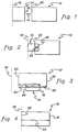
- FIG. 1 is a block diagram of a layout of two objects spaced a distance apart.
- FIG. 2 is a block diagram of a layout of the objects of FIG. 1 merged together.
- FIG. 3 is a block diagram of a layout of the objects of FIG. 1 overlapping.
- FIG. 4 is a block diagram of one of the objects of FIG. 1 showing a size constraint therefor.
- FIG. 5 is a block diagram of a layout of three objects with insufficient spacing between them.
- FIG. 6 is a block diagram of the layout of FIG. 5 after moving two of the objects to accommodate the third in accordance with the present invention.
- FIG. 7 is a general flow diagram for the minimum perturbation method of the first aspect of the present invention.
- FIG. 8 is a block diagram of a layout of three objects with a fourth to be inserted between two of them.
- FIG. 9 is a block diagram of the layout of FIG. 8 modified to include the fourth object, resulting in design violations.
- FIG. 10 is a block diagram of the layout of FIG. 9 modified to remove the design violations in accordance with the present invention.
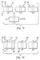
- FIG. 11 is a block diagram of a layout of three transistors and a fourth to be inserted therein.
- FIG. 12 is a block diagram of the layout of FIG. 11 with one of the three transistors and the fourth merged in accordance with the present invention.
- FIG. 13 is a block diagram of the layout of FIG. 11 with two of the three transistors and the fourth merged in accordance with the present invention.
- FIG. 14 is a block diagram of a hierarchical device layout and a transistor to be inserted therein.
- FIG. 15 is a block diagram of the hierarchical layout of FIG. 14 after insertion of the transistor in accordance with the present invention.
- FIG. 16 is a block diagram of a layout of three integrated circuit devices prior to aligning two of them in accordance with the present invention.
- FIG. 17 is a flow diagram for a portion of the automatic global optimization technique of the second aspect.
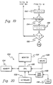
- FIGs. 18 and 19 together are a flow diagram for another portion of the automatic global optimization technique of the second aspect.
- FIG. 20 is a block diagram of a workstation implementing the present invention in the form of a computer program in accordance with a third aspect.
- Symbolic entry allows the designer to manipulate device placement (and routing) in a symbolic form, representing the individual devices as objects of representative size and wires as sticks of zero width.
- the designer supplies only gross topological information without concern for the actual device sizes, wire sizes or the technology design rules, such as inter-device spacing.
- the symbolic layout is then compacted using the actual device and wire sizes along with the design rules.
- the compaction produces unexpected results and limits designer control over the final product, requiring the addition of constraints by the designer.
- the symbolic approach may hide useful data from the designer critical to design decisions, such as device size.
- the present invention automates many of the tedious parts of object placement while maintaining the full flexibility of custom layout design.
- the automation incorporates a minimum perturbation technique that incrementally corrects the layout after each manual edit operation using the smallest possible modification. This enables the designer to explore a larger number of legal placement configurations in a given time than was previously possible.
- the result of the present invention is an improved layout quality and greatly enhanced designer productivity. Subsequently, the present invention will be described with reference to integrated circuit (hereinafter, "IC") design, however, it will be understood that it is meant to be applied in other areas of object placement.
- IC integrated circuit
- an IC layout comprises a list of devices, for example, transistors, their positions, fixed circuit elements in the image, such as power and ground buses, and possible movable elements attached to the devices, such as wires.
- devices for example, transistors, their positions, fixed circuit elements in the image, such as power and ground buses, and possible movable elements attached to the devices, such as wires.
- layout consisting of only devices.
- displayout will be used herein as both a list of elements and a visual representation thereof.
- the present exemplary embodiment models a given device within a layout as a collection of shapes which can be manipulated as a whole, but not independently.
- an IC device as a rectangular block with ports representing the external wiring contacts, e.g., a transistor's source, drain and gate. Each port is associated with a net attribute describing its connectivity to other ports.
- the ports falling on the device boundary are marked explicitly, and inter-device placement adheres to design rules by maintaining constraints between boundary edges of the devices. Positions of shapes within a device are fixed with respect to its boundary, and constraints between shapes of different devices can be translated to constraints between boundary edges of the corresponding devices.
- the adjacency relations between device edges is recorded using two constraint lists, one for the horizontal relations and one for the vertical relations. Constraints for device spacing, overlap, intersection and device size are derived by traversing the relations in the lists, analogous to traversing the layout horizontally and vertically.
- FIGs. 1-4 depict the different types of horizontal relations, it being understood that the vertical are similar.
- FIG. 1 depicts object 10 and object 12 spaced apart by a distance 14.
- the position of right edge 16 of object 10 with respect to arbitrary reference 18 is denoted x (10,r)
- the position of left edge 20 of object 12 is denoted x (12,l) .
- FIG. 2 depicts objects 10 and 12 from FIG. 1 merged together by a distance 22, denoted by merge_dist (10,12) .
- merge_dist 10,12
- FIG. 3 depicts object 10 intersected with object 12, the intersection defined by a distance 24 between the left edge 20 of object 12 and the right edge 16 of object 10, and a distance 26 between left edge 28 of object 10 and right edge 30 of object 12.
- Distance 24 is denoted intersection_dist1
- distance 26 is denoted intersection_dist2.
- x (10,r) - x (12,l) > intersection_dist1
- x (12,r) - x (10,l) > intersection_dist2. It should be noted that usually, two objects intersecting horizontally also intersect vertically.
- FIG. 5 depicts a simple layout 33 comprising generic objects 34, 36 and 38, where objects 34 and 36 are separated by a distance 40 and objects 36 and 38 are separated by a distance 42.
- Distance 40 can be described as the distance between left edge 46 of device 36 and right edge 44 of device 34. Edges 44 and 46 have distance values relative to arbitrary reference 48. Assume that distances 40 and 42 are insufficient, according to design rules for such objects.
- the violation with respect to distance 40 x (36,l) - x (34,r) ⁇ min_dist (34,36) .
- the violation with respect to distance 42 can be expressed as: x (38,l) - x (36,r) ⁇ min_dist (36,38) .
- the end result of correcting the violations using the present invention is to modify layout 33 to comply with the design rules such that to the greatest extent possible, the movement of objects 34, 36 and 38 is minimized; that is, perturbation thereof is minimized. More specifically, the objective is to find new locations for the edges of objects 34, 36 and 38 such that the constraint violations are removed, i.e., the resulting layout is "legal", and such that a given edge is only moved if absolutely necessary. This first requires a definition for two groupings of edges that will be used.
- the LEFTSET of edges is defined as the left-most edge in the right-most violation pair together with all transitive left neighbors thereof.
- the right-most violation pair is the right edge 50 of object 36 and the left edge 52 of object 38.
- "transitive” means each successive edge moving left away from edge 50 where the vertical span thereof coincides with the vertical span of the immediately previous edge. For example, if in layout 33 it was a constraint that object 34 must stay in its present location with respect to reference 48, then objects 36 and 38 would have to be moved to the right to remove the violations. In the present example, there are no such constraints. Thus, the LEFTSET contains edges 50, 46, 44 and 54.
- the RIGHTSET of edges is defined as the right-most edge in the left-most violation pair together with all transitive right neighbors thereof.
- the left-most violation pair is the right edge 44 of object 34 and the left edge 46 of object 36.
- the RIGHTSET consists of edges 46, 50, 52 and 56. Note that with multiple violations in a given layout, as in the present example, it is possible for a given edge to be both in the LEFTSET and the RIGHTSET.
- edges 46 and 50 are in both the LEFTSET and RIGHTSET.
- edges only in the LEFTSET may move, if at all, only to the left of their present position with respect to reference 48.
- this constraint pertains to edges 44 and 54, and is reflected in constraint (c) below.
- edges only in the RIGHTSET may only move, if at all, only to the right of their present position with respect to reference 48.
- this constraint pertains to edges 52 and 56, and is reflected in constraint (d) below. Edges in both the LEFTSET and the RIGHTSET have no additional movement constraints (although there may be user constraints), and edges in neither set must remain in their current position.
- FIG. 6 depicts the resultant layout 58 of minimizing P while satisfying the above system of linear constraints. It will be understood that usually in practice, a similar exercise would be performed in the vertical direction not necessary in this simplified example. As compared to FIG. 5, object 34 has been moved in FIG. 6 to the left a distance 60 and object 38 has been moved to the right a distance 62. As one skilled in the art will know, any number of techniques could be used to solve the above minimum perturbation equation subject to the above linear constraints, for example, simplex (see Papadimitrou and Steiglitz, Combinational Optimization Algorithms and Complexity , pgs. 25-62, Prentice Hall, 1982) or a heuristic technique such as the constraint lists used herein. Where there are multiple equivalent solutions, the method of solution will determine the outcome.
- FIG. 6 and the description thereof above is a visual example of object insertion using the minimum perturbation method of the first aspect. More specifically, FIG. 7 is a flow diagram of the steps of the minimum perturbation method that begin with deriving the horizontal and vertical constraint lists (STEP 136, "DERIVE CONSTRAINT MODEL"). Then, any violations due to the device insertion are uncovered (STEP 138, "DETERMINE VIOLATIONS") by comparing the constraint lists to the design rules. From the determined violations, the LEFTSET and RIGHTSET are determined (STEP 140, "DETERMINE LEFTSET AND RIGHTSET").
- the minimum perturbation equation is then solved for (STEP 142, "DETERMINE MINIMUM PERTURBATION") and, finally, the layout is modified in accordance with the solution to the minimum perturbation equation (STEP 144, "MODIFY LAYOUT").
- FIG. 8 is a block diagram of a layout 200 of three objects 202, 204 and 206. Assume that a fourth object 208 is to be inserted between objects 202 and 204. Each object in FIG. 8 is two units wide, according to scale 210, and the left edge 212 of object 202 is located at position 2 with respect to reference 213, the left edge 214 of object 204 is located at position 8 and the left edge 216 of object 206 is located at position 12. Assume also that the minimum allowable inter-object spacing is two units.
- the first scenario is that objects 204 and 206 are moved one unit to the right and object 202 is moved one unit to the left.
- the second scenario is that object 202 remains in place, while objects 204 and 206 each move 2 units to the right, assuming we place the left edge of object 208 at position 6.
- the third scenario is that object 202 is moved 2 units to the left, while objects 204 and 206 remain in their current positions, assuming that the left edge of object 208 is placed at position 4. Since our goal is to move the least number of objects the least amount, in this simple example we intuitively know that the third scenario is preferred.
- FIG. 9 depicts the objects of FIG. 8 in a modified layout 201 with the fourth object inserted midway between objects 202 and 204. Traversing modified layout 201 from left to right horizontally, we first obtain a horizontal constraint model. Note that in this simplified example, there is no vertical constraint model necessary.
- the constraint model comprises the following entries:
- the violations are noted: x (208,l) - x (202,r) ⁇ min_dist (202,208) ; and x (204,l) - x (208,r) ⁇ min_dist (204,208) , and the LEFTSET and RIGHTSET are defined: LEFTSET : x (208,r) , x (208,l) , x (202,r) and x (202,l) ; RIGHTSET: x (208,l) , x (208,r) , x (204,l) , x (204,r) , x (206,l) and x (206,r) .
- the present invention When used specifically with IC layout design, the present invention supports several different types of layout modifications, including insertion and deletion of a device, device merging, merged device manipulation, hierarchical placement manipulation, space insertion and deletion and structure alignment.
- the present invention has been found to be useful in automatic object placement, as will be described subsequently with reference to a second aspect of the invention.
- FIG. 11 is a block diagram of a layout 63 of transistors 64, 66 and 68 spaced apart in relation to arbitrary reference 71. Assume that a constraint list exists for layout 63 and that it is desired to insert transistor 70 between devices 64 and 66.
- FIG. 12 depicts a new layout 76 from the results of solving the minimum perturbation system of linear equations.
- Transistors 66 and 68 have been moved to the right with respect to reference 71, transistors 64 and 70 have been merged along common diffusion region 78 and transistor 64 has been moved to the left with respect to reference 71.
- the edges of diffusion regions 72 and 74 remain distinct after the merger thereof, however, merged diffusion regions 72 and 74 could be reconstrained as a single common diffusion region 78.
- transistor 64 If we assume it is desired to have transistor 64 remain in place, then we place transistor 70 such that it merges with transistor 64 and place transistor 66 such that it merges with transistor 70. Violations are then found and used to define LEFTSET and RIGHTSET. After solving the minimum perturbation system of linear equations, the new layout 84 is created. Transistors 66 and 68 have moved farther to the right with respect to reference 71 than in FIG. 12 and common diffusion region 86 has been created.
- Hierarchical portion 88 of a device layout shown in FIG. 14.
- Hierarchical portion 88 comprises device 90, pseudo-device 92 and device 94.
- Pseudo-device 92 comprises transistors 96 and 98.
- transistor 100 Assume that it is desired to insert transistor 100 between devices 96 and 98, and that such insertion presents merging opportunities for device 100 with both devices 96 and 98.
- Device 100 is inserted, the resulting violations are found, LEFTSET and RIGHTSET are defined and the minimum perturbation equation is solved to find a placement for device 100 within pseudo device 92, which is the "sub-layout" in question at this point.
- FIG. 15 depicts the result of the hierarchical minimum perturbation technique, with devices 90 and 96 moving to the left with respect to reference 102, and devices 94 and 98 moving to the right with respect to reference 102. This process can be used over an arbitrary depth of hierarchy.
- Space insertion may be desirable in some situations, for example, to improve routeability at the next level of hierarchy or to allow for future modifications. Inserting may be accomplished by inserting an imaginary device with the appropriate dimensions. The device insertion routine is then followed as described above.
- the removal of unwanted space in a layout is accomplished by solving the minimum perturbation routine to reduce the space to the design rule minimum.
- distance 14 is too large; that is, we want to reduce distance 14 to the minimum design rule for inter-device spacing of devices 10 and 12.
- Device 12 is first moved to its left-most legal position with respect to device 10. This can readily be found from the existing horizontal constraint list. Alternately, device 10 could be moved to its right-most legal position with respect to device 12, or both devices could be moved toward one another such that inter-device spacing thereof is the legal minimum. Next, design rule violations are searched for, LEFTSET and RIGHTSET are determined and the minimum perturbation is found. This incremental removal of unwanted space allows the designer to retain much more control than global space removal methods, such as compaction.
- Another useful design feature supported by the present invention is structural alignment.
- layout 104 in FIG. 16 comprising transistor 106, transistor 108 and device 110.
- transistor 106 Assume that it is desired to align the left edge of gates 112 and 114, edges 116 and 118, respectively, along reference 120. Moving transistor 108 to the left with respect to reference 120 would require the movement of device 110. Thus, the alignment will lead to design rule violations.
- transistors 106 and 108 are aligned, the induced violations and LEFTSET and RIGHTSET are found and the minimum perturbation is determined.
- the goal of the toss method is to automatically place a device selected by the designer optimally within the current layout.
- "Optimally" in the present embodiment is with respect to a cost function, having three basic components, used to measure layout quality quantitatively.
- the first component is a merge term, designed to maximize diffusion sharing, formulated as total area of diffusion minus merged area of diffusion.
- the second component is an alignment term, designed to improve density, routeability and aesthetics by encouraging appropriate structural alignments. Aligning devices within a given layout facilitates routing of wires, providing as straight a path as possible with the least number of obstacles.
- the third component is a net (electrical net) cost term, designed to minimize the length of wire required to connect the placed devices, improving performance and routeability.
- a routing estimator is used instead.
- One such exemplary estimator is a Full Geometry Minimum Spanning Tree (FGMST), as described in J. Cohn et al., Analog Device Level Layout Automation , Kluwer Press, Boston, 1993.
- the FGMST estimator seeks to determine the shortest path connecting all terminals of an electrical net.
- the FGMST estimator extends a basic minimum spanning tree, which one skilled in the art will already know, to take advantage of the full geometry of the connected device terminals.
- This FGMST estimator measures the minimum distance between a collection of shapes of any rectilinear geometry using an extension to Primm's algorithm.
- Primm's algorithm One skilled in the art will be familiar with Primm's algorithm.
- the FGMST distance between connected terminals goes to zero when the terminals touch, i.e, merge, in any manner. Not only does this eliminate the conservative placement associated with center-measured minimum spanning trees, but it effectively allows terminal geometry to form edges in the spanning tree. This more accurately models an automated router's ability to use device terminal geometry as part of its routing path. The result is a much more accurate prediction of the routed length of the net.
- cost function could be weighted toward a particular component in a given situation.
- additional components may easily be incorporated, such as, for example, layout area and/or aspect ratio.
- the cost function could be weighted toward a particular component in a given situation.
- the device is placed exhaustively in every location where it can be merged.
- all legal orientations of the device where a merger is possible are attempted, pushing aside other devices as necessary using the minimum perturbation method of the first aspect.
- the preferred legal orientations comprise 90 degree rotations from the horizontal with the mirror of each.
- the cost function is evaluated and the lowest cost is tracked along with the corresponding location and orientation.
- FIG. 17 is a flow diagram for the mergeable solution portion of the global placement optimization method of the second aspect.
- M denoting the total number
- a counter C for the cost function is also initialized to some large number (STEP 140, "INITIALIZE COST C").
- the chosen device is placed at location M in orientation L (STEP 142, "PLACE DEVICE AT M, L").
- Step 142 may require for any given location or orientation, that one or more other devices are pushed aside, which is accomplished using the minimum perturbation method of the first aspect.
- the cost function is determined (STEP 144, "DETERMINE COST").
- An inquiry is then made as to whether the determined cost is less than the counter C (INQUIRY 146, "COST ⁇ C?").
- a predictor is used to find an "optimal" position for the chosen device.
- "optimal” refers to a location likely to provide the shortest routing.
- the preferred method for determining the "optimal" location in IC design is a quadratic net cost, presented in Tsai et al., PROUD: A Sea-of-Gates Placement Algorithm , IEEE Design and Test, December, 1988. However, it will be understood that other estimators could be used.
- the Tsai et al. quadratic net cost can be thought of as treating each device already in an electrical net as fixed and connected to all other devices in the net by rubber bands or springs.
- quadratic net cost An advantage of the quadratic net cost is that the minimum total wire length can be solved for exactly, since the quadratic net cost is a well-defined function, by setting the derivative of the formula to zero and solving for the length. Although the quadratic net cost yields a good starting point from where to look for the final position, it is not considered to be useful as the final location, as it is overly conservative. There would be significantly less wires (or rubber bands) used in a real IC design; not all devices would be directly electrically connected. In the non-mergeable situation, an exhaustive search for the lowest cost location is impractical, unlike the mergeable situation where there are a manageably finite number of possibilities. Therefore, the "optimal" position serves as a reasonable (though not perfect) starting point.
- the chosen device is placed in the optimal position in all legal orientations without regard to alignment considerations, pushing aside other existing devices when necessary using the method of the first aspect.
- the cost function is determined and the lowest is tracked.
- a visibility search for devices in the vicinity of the optimal position are found and all possible alignments therewith are attempted along with all legal orientations at each possible alignment, with the cost function for each attempt being evaluated and the lowest tracked.
- the phrase "in the vicinity of" used in the preceding sentence refers to a search in all chosen directions (here, there are four - above, below, left and right) for a predetermined distance in each direction. If no devices are found within those constraints, then the current lowest cost position and orientation is returned as the final position. Finally, the lowest cost configuration among the mergeable and non-mergeable solutions is returned as the solution.
- FIGs. 18 and 19 are together a flow diagram for the non-mergeable portion of global placement optimization according this second aspect.
- the "optimal" position is determined for the chosen device to be added to the current layout (STEP 158, "DETERMINE 'OPTIMAL' POSITION).
- an inquiry is made as to whether the maximum number of legal orientations has been exceeded (INQUIRY 174, "L > MAXIMUM?"). If there are still available legal orientations, the routine returns to STEP 164. If there are no more legal orientations remaining, the visibility search is performed at the "optimal" position (STEP 176, "PERFORM VISIBILITY SEARCH”) to find all possible alignments within a predetermined distance in each direction. An inquiry is made after the visibility search to determine if any alignment opportunities were discovered (INQUIRY 178, "ANY ALIGNMENTS?”).
- the device is placed at the location for the current alignment and orientation (STEP 184, "PLACE DEVICE AT A, L"), which may require that the minimum perturbation routine of the first aspect be used.
- the cost function is determined (STEP 186, "DETERMINE COST").
- toss optimization is useful for a single device placement.
- sequential automatic placement is used to achieve a reasonable placement by applying toss sequentially to each device as a layout is created.
- the order of device placement could be selected by the designer or chosen automatically based on an arbitrary number of criteria (e.g., random ordering or connectivity).
- the layout becomes more dense.
- the push-aside features of the first aspect tend to mitigate the effects thereof.
- the quality of the layout would directly depend on the order in which the devices are placed, which cannot be globally known to any useful extent prior to trial placement.
- an additional iterative relaxation placement phase may be added.
- each device in a completed layout is subjected to the toss optimization a number of times until no further improvement is noted (based on predetermined criteria) or the designer stops the process.
- a device when a device is removed, either a "hole" could be left where the device was, or the hole could be filled in with the rest of the objects in the layout, for example, via compaction.
- whether or not the hole is left in a given situation could be an option for the designer.
- the hole is left there, as this is in keeping with the goal of minimum perturbation, i.e., minimizing the movement of objects in a layout.
- the order in which the devices are selected may be, for example, random or, as another example, calculated by selecting the devices most distant from their "optimal" location.
- FIG. 20 depicts a generic workstation 122, including monitor 124, central processing unit 126, mouse 128, disk drive 130, keyboard 132 and memory 134.
- monitor 124 central processing unit 126
- mouse 1208 disk drive 130
- keyboard 132 and memory 134 disk drives 130
- FIG. 20 depicts a generic workstation 122, including monitor 124, central processing unit 126, mouse 128, disk drive 130, keyboard 132 and memory 134.
- workstation 122 includes disk drive 130, other types of auxiliary storage may be used, such as optical storage devices.
- the functions of keyboard 132 and mouse 128 could be accomplished by a touch screen monitor, a pen-based interactive apparatus or even with voice or other sound-based apparatus.
- Mouse 128 could also be replaced with some other type of pointing device, and keyboard 132 could be replaced by other types of input devices.
- the present invention could, for example, be implemented in a computer program on disk 136 accessed by CPU 126 via disk drive 130. The user then manipulates a layout using keyboard 132 and/or mouse 128.
- One skilled in the art will know how to implement the present invention in a computer program and the details of workstation 122 operation.
Landscapes
- Engineering & Computer Science (AREA)
- Physics & Mathematics (AREA)
- Theoretical Computer Science (AREA)
- Computer Hardware Design (AREA)
- General Physics & Mathematics (AREA)
- Geometry (AREA)
- General Engineering & Computer Science (AREA)
- Evolutionary Computation (AREA)
- Computational Mathematics (AREA)
- Pure & Applied Mathematics (AREA)
- Mathematical Optimization (AREA)
- Mathematical Analysis (AREA)
- Computer Networks & Wireless Communication (AREA)
- Design And Manufacture Of Integrated Circuits (AREA)
Applications Claiming Priority (2)
| Application Number | Priority Date | Filing Date | Title |
|---|---|---|---|
| US253898 | 1981-04-13 | ||
| US08/253,898 US5535134A (en) | 1994-06-03 | 1994-06-03 | Object placement aid |
Publications (2)
| Publication Number | Publication Date |
|---|---|
| EP0685804A2 true EP0685804A2 (de) | 1995-12-06 |
| EP0685804A3 EP0685804A3 (de) | 1996-03-27 |
Family
ID=22962155
Family Applications (1)
| Application Number | Title | Priority Date | Filing Date |
|---|---|---|---|
| EP95480066A Withdrawn EP0685804A3 (de) | 1994-06-03 | 1995-05-19 | Platzierungshilfe für Objekte. |
Country Status (3)
| Country | Link |
|---|---|
| US (1) | US5535134A (de) |
| EP (1) | EP0685804A3 (de) |
| JP (1) | JP2886481B2 (de) |
Cited By (4)
| Publication number | Priority date | Publication date | Assignee | Title |
|---|---|---|---|---|
| EP1146393A3 (de) * | 2000-04-10 | 2005-07-20 | Infineon Technologies AG | Verfahren zur Herstellung von Masken für die Fertigung von Halbleiterstrukturen |
| DE102004038063A1 (de) * | 2004-07-30 | 2006-03-23 | Infineon Technologies Ag | Verfahren zur Herstellung einer Standardzellenanordnung und eine Vorrichtung zur Durchführung des Verfahrens |
| WO2011131459A1 (de) * | 2010-04-23 | 2011-10-27 | Siemens Aktiengesellschaft | Verfahren zur eingabe eines räumlichen aufbaus von fertigungseinrichtungen in ein rechnergestütztes planungsprogramm und dessen optimierung |
| CN113710314A (zh) * | 2019-04-01 | 2021-11-26 | 皇家飞利浦有限公司 | 用于局灶治疗处置的处置规划 |
Families Citing this family (65)
| Publication number | Priority date | Publication date | Assignee | Title |
|---|---|---|---|---|
| JP3202490B2 (ja) * | 1994-07-22 | 2001-08-27 | 株式会社東芝 | 集積回路のレイアウト方法及び集積回路のレイアウト装置 |
| JPH08227428A (ja) * | 1995-02-20 | 1996-09-03 | Matsushita Electric Ind Co Ltd | プリント基板cad装置 |
| US5901065A (en) * | 1996-02-07 | 1999-05-04 | Motorola, Inc. | Apparatus and method for automatically placing ties and connection elements within an integrated circuit |
| US6035108A (en) * | 1996-10-17 | 2000-03-07 | Nec Corporation | Figure layout compaction method and compaction device |
| US5943243A (en) * | 1996-10-28 | 1999-08-24 | International Business Machines Corporation | Method and system for removing hardware design overlap |
| US6374200B1 (en) * | 1997-02-03 | 2002-04-16 | Fujitsu Limited | Layout apparatus for laying out objects in space and method thereof |
| US5953518A (en) * | 1997-03-14 | 1999-09-14 | Lsi Logic Corporation | Yield improvement techniques through layout optimization |
| US6240466B1 (en) | 1997-04-21 | 2001-05-29 | International Business Machines Corporation | Object-oriented apparatus and method for determining new object location relative to an existing object |
| US5943497A (en) * | 1997-04-30 | 1999-08-24 | International Business Machines Corporation | Object-oriented apparatus and method for controlling configuration of object creation |
| US6122443A (en) * | 1997-07-28 | 2000-09-19 | Kabushiki Kaisha Toshiba | Wire length minimization apparatus and method |
| US6449761B1 (en) | 1998-03-10 | 2002-09-10 | Monterey Design Systems, Inc. | Method and apparatus for providing multiple electronic design solutions |
| US6446239B1 (en) * | 1998-03-10 | 2002-09-03 | Monterey Design Systems, Inc. | Method and apparatus for optimizing electronic design |
| US6189132B1 (en) | 1998-04-09 | 2001-02-13 | International Business Machines Corporation | Design rule correction system and method |
| US6658634B1 (en) * | 1998-05-07 | 2003-12-02 | International Business Machines Corporation | Logic power optimization algorithm |
| DE69811127T2 (de) * | 1998-11-30 | 2003-11-20 | Actcon Control Ab, Hisings Backa | Verfahren um objekte in den arbeitsbereich in eine rechneranwendung einzubringen |
| US6424959B1 (en) * | 1999-06-17 | 2002-07-23 | John R. Koza | Method and apparatus for automatic synthesis, placement and routing of complex structures |
| JP3453535B2 (ja) * | 1999-08-03 | 2003-10-06 | 松下電器産業株式会社 | 自動配線設計における配線経路探索方法及び配線経路探索プログラムを記録した記録媒体 |
| JP2001060663A (ja) * | 1999-08-20 | 2001-03-06 | Nec Corp | 半導体集積回路装置 |
| US6351841B1 (en) * | 2000-03-21 | 2002-02-26 | Cadence Design Systems, Inc. | Method and apparatus for creating multi-gate transistors with integrated circuit polygon compactors |
| JP2002305223A (ja) * | 2001-04-05 | 2002-10-18 | Toshiba Corp | 半導体装置における座標変換システム、及び座標変換プログラム |
| EP1405228B1 (de) | 2001-06-29 | 2012-09-05 | Cadence Design Systems, Inc. | Zweidimensionales kompaktierungssystem und verfahren |
| US6789233B2 (en) * | 2002-08-28 | 2004-09-07 | Micron Technology, Inc. | Method for determining a matched routing arrangement for semiconductor devices |
| US8798964B2 (en) * | 2002-11-06 | 2014-08-05 | Hewlett-Packard Development Company, L. P. | Methods and apparatus for designing the racking and wiring configurations for pieces of hardware |
| US7200827B1 (en) * | 2003-05-14 | 2007-04-03 | Apex Design Systems, Inc. | Chip-area reduction and congestion alleviation by timing-and-routability-driven empty-space propagation |
| US20050086622A1 (en) * | 2003-10-16 | 2005-04-21 | International Business Machines Corporation | Hybrid quadratic placement with multiple linear system solvers |
| US7111264B2 (en) * | 2003-10-17 | 2006-09-19 | Lsi Logic Corporation | Process and apparatus for fast assignment of objects to a rectangle |
| US7036102B2 (en) * | 2003-10-27 | 2006-04-25 | Lsi Logic Corporation | Process and apparatus for placement of cells in an IC during floorplan creation |
| US7103865B2 (en) * | 2003-11-21 | 2006-09-05 | Lsi Logic Corporation | Process and apparatus for placement of megacells in ICs design |
| US7103858B2 (en) * | 2004-04-14 | 2006-09-05 | Lsi Logic Corporation | Process and apparatus for characterizing intellectual property for integration into an IC platform environment |
| US7448012B1 (en) | 2004-04-21 | 2008-11-04 | Qi-De Qian | Methods and system for improving integrated circuit layout |
| US7210113B2 (en) * | 2004-04-23 | 2007-04-24 | Lsi Logic Corporation | Process and apparatus for placing cells in an IC floorplan |
| TW200538919A (en) * | 2004-05-21 | 2005-12-01 | Hon Hai Prec Ind Co Ltd | System and method for checking split plane of motherboard layout |
| US8510657B2 (en) * | 2004-09-30 | 2013-08-13 | Microsoft Corporation | Editing the text of an arbitrary graphic via a hierarchical list |
| US8134575B2 (en) | 2004-09-30 | 2012-03-13 | Microsoft Corporation | Maintaining graphical presentations based on user customizations |
| US7348982B2 (en) | 2004-09-30 | 2008-03-25 | Microsoft Corporation | Method, system, and computer-readable medium for creating and laying out a graphic within an application program |
| US7302651B2 (en) | 2004-10-29 | 2007-11-27 | International Business Machines Corporation | Technology migration for integrated circuits with radical design restrictions |
| US7310786B2 (en) * | 2005-02-03 | 2007-12-18 | Springsoft, Inc. | IC compaction system |
| US8438486B2 (en) | 2006-02-09 | 2013-05-07 | Microsoft Corporation | Automatically converting text to business graphics |
| US7454721B2 (en) * | 2006-02-27 | 2008-11-18 | International Business Machines Corporation | Method, apparatus and computer program product for optimizing an integrated circuit layout |
| US20070257903A1 (en) * | 2006-05-04 | 2007-11-08 | Harris Corporation | Geographic information system (gis) for displaying 3d geospatial images with reference markers and related methods |
| US7590955B1 (en) * | 2006-06-28 | 2009-09-15 | Cadence Design Systems, Inc. | Method and system for implementing layout, placement, and routing with merged shapes |
| US7761819B2 (en) * | 2006-07-05 | 2010-07-20 | Yue Yang | System and method of modification of integrated circuit mask layout |
| US7735042B2 (en) * | 2007-08-01 | 2010-06-08 | International Business Machines Corporation | Context aware sub-circuit layout modification |
| US7937682B2 (en) * | 2008-01-31 | 2011-05-03 | Synopsys, Inc. | Method and apparatus for automatic orientation optimization |
| US9092110B2 (en) * | 2008-12-16 | 2015-07-28 | Cadence Design Systems, Inc. | Method and system for implementing a user interface with ghosting |
| US8799325B2 (en) | 2010-03-12 | 2014-08-05 | Microsoft Corporation | Reordering nodes in a hierarchical structure |
| US8893048B2 (en) | 2011-05-13 | 2014-11-18 | Kalyan M. Gupta | System and method for virtual object placement |
| US8782585B2 (en) * | 2011-07-13 | 2014-07-15 | The Regents Of The University Of California | Methods for integrated circuit C4 ball placement |
| US8984467B2 (en) | 2011-08-17 | 2015-03-17 | Synopsys, Inc. | Method and apparatus for automatic relative placement generation for clock trees |
| US8806389B2 (en) * | 2011-10-20 | 2014-08-12 | Asml Netherlands B.V. | Method and apparatus for model based flexible MRC |
| US9003349B1 (en) | 2013-06-28 | 2015-04-07 | Cadence Design Systems, Inc. | Methods, systems, and articles of manufacture for implementing a physical electronic design with area-bounded tracks |
| US8984465B1 (en) | 2013-06-28 | 2015-03-17 | Cadence Design Systems, Inc. | Methods, systems, and articles of manufacture for automatically assigning track patterns to regions for physical implementation of an electronic design |
| US9117052B1 (en) | 2012-04-12 | 2015-08-25 | Cadence Design Systems, Inc. | Methods, systems, and articles of manufacture for interactively implementing physical electronic designs with track patterns |
| US9251299B1 (en) * | 2013-06-28 | 2016-02-02 | Cadence Design Systems, Inc. | Methods, systems, and articles of manufacture for associating track patterns with rules for electronic designs |
| US9075932B1 (en) | 2012-08-31 | 2015-07-07 | Candence Design Systems, Inc. | Methods and systems for routing an electronic design using spacetiles |
| US9104830B1 (en) | 2013-06-28 | 2015-08-11 | Cadence Design Systems, Inc. | Methods, systems, and articles of manufacture for assigning track patterns to regions of an electronic design |
| US9183343B1 (en) * | 2012-08-31 | 2015-11-10 | Cadence Design Systems, Inc. | Methods, systems, and articles of manufacture for implementing high current carrying interconnects in electronic designs |
| US9213793B1 (en) | 2012-08-31 | 2015-12-15 | Cadence Design Systems, Inc. | Methods, systems, and articles of manufacture for implementing electronic designs using flexible routing tracks |
| US8935649B1 (en) | 2012-08-31 | 2015-01-13 | Cadence Design Systems, Inc. | Methods, systems, and articles of manufacture for routing an electronic design using spacetiles |
| US9817941B2 (en) | 2012-12-04 | 2017-11-14 | Cadence Design Systems, Inc. | Methods, systems, and articles of manufacture for implementing high current carrying interconnects in electronic designs |
| US9165103B1 (en) | 2013-06-28 | 2015-10-20 | Cadence Design Systems, Inc. | Methods, systems, and articles of manufacture for tessellating and labeling routing space for routing electronic designs |
| US9361417B2 (en) | 2014-02-07 | 2016-06-07 | Synopsys, Inc. | Placement of single-bit and multi-bit flip-flops |
| US11531794B1 (en) * | 2019-12-20 | 2022-12-20 | Ansys, Inc. | Voltage drop analysis using local circuit representation |
| US11663388B1 (en) | 2019-12-20 | 2023-05-30 | Ansys, Inc. | DVD simulation using microcircuits |
| JP7344149B2 (ja) * | 2020-02-07 | 2023-09-13 | キオクシア株式会社 | 最適化装置及び最適化方法 |
Family Cites Families (39)
| Publication number | Priority date | Publication date | Assignee | Title |
|---|---|---|---|---|
| FR1502554A (de) * | 1965-12-01 | 1968-02-07 | ||
| US3617714A (en) * | 1969-04-15 | 1971-11-02 | Bell Telephone Labor Inc | Method of minimizing the interconnection cost of linked objects |
| US4551810B1 (en) * | 1982-07-28 | 1995-09-05 | Technology Inc Const | Method and apparatus for designing duct work for producing patterns for conduit sections in the designated duct work |
| US4639604A (en) * | 1983-03-29 | 1987-01-27 | Nippon Kagaku K.K. | Method and apparatus for detecting an edge position of a pattern and eliminating overlapping pattern signals |
| US4554625A (en) * | 1983-06-14 | 1985-11-19 | International Business Machines Corporation | Method for generating an optimized nested arrangement of constrained rectangles |
| US4577276A (en) * | 1983-09-12 | 1986-03-18 | At&T Bell Laboratories | Placement of components on circuit substrates |
| US4630219A (en) * | 1983-11-23 | 1986-12-16 | International Business Machines Corporation | Element placement method |
| JPS60114968A (ja) * | 1983-11-28 | 1985-06-21 | Hitachi Ltd | 推論システム |
| US4686629A (en) * | 1984-05-10 | 1987-08-11 | Rca Corporation | Logic cell placement method in computer-aided-customization of universal arrays and resulting integrated circuit |
| JPH0679319B2 (ja) * | 1985-04-10 | 1994-10-05 | 株式会社日立製作所 | 配置更新方法 |
| US4754408A (en) * | 1985-11-21 | 1988-06-28 | International Business Machines Corporation | Progressive insertion placement of elements on an integrated circuit |
| US5175696A (en) * | 1986-09-12 | 1992-12-29 | Digital Equipment Corporation | Rule structure in a procedure for synthesis of logic circuits |
| US4908772A (en) * | 1987-03-30 | 1990-03-13 | Bell Telephone Laboratories | Integrated circuits with component placement by rectilinear partitioning |
| US4812962A (en) * | 1987-04-09 | 1989-03-14 | Harris Corp. | Area feature sorting mechanism for neighborhood-based proximity correction in lithography processing of integrated circuit patterns |
| US4918614A (en) * | 1987-06-02 | 1990-04-17 | Lsi Logic Corporation | Hierarchical floorplanner |
| US4815003A (en) * | 1987-06-19 | 1989-03-21 | General Electric Company | Structured design method for high density standard cell and macrocell layout of VLSI chips |
| US4922432A (en) * | 1988-01-13 | 1990-05-01 | International Chip Corporation | Knowledge based method and apparatus for designing integrated circuits using functional specifications |
| DE58907307D1 (de) * | 1988-11-02 | 1994-04-28 | Siemens Ag | Verfahren zur plazierung von modulen auf einem träger. |
| JP2536125B2 (ja) * | 1989-02-15 | 1996-09-18 | 日本電気株式会社 | 配置処理方式 |
| JPH02242474A (ja) * | 1989-03-16 | 1990-09-26 | Hitachi Ltd | 素子配置最適化方法及び装置並びに最適配置判定方法及び装置 |
| JP2863550B2 (ja) * | 1989-06-08 | 1999-03-03 | 株式会社日立製作所 | 配置最適化方法及び配置最適化装置と回路設計装置 |
| JP2831703B2 (ja) * | 1989-06-23 | 1998-12-02 | 株式会社東芝 | 自動フロアプラン演算装置 |
| US5231590A (en) * | 1989-10-13 | 1993-07-27 | Zilog, Inc. | Technique for modifying an integrated circuit layout |
| JP2895129B2 (ja) * | 1990-01-22 | 1999-05-24 | 株式会社東芝 | 論理セルの配置処理方法及び論理セルの配置処理装置 |
| JP3032224B2 (ja) * | 1990-02-21 | 2000-04-10 | 株式会社東芝 | 半導体集積回路の論理セル配置方法 |
| US5218551A (en) * | 1990-04-30 | 1993-06-08 | International Business Machines Corporation | Timing driven placement |
| JPH0456341A (ja) * | 1990-06-26 | 1992-02-24 | Matsushita Electric Ind Co Ltd | 半導体集積回路のレイアウト方法 |
| US5224056A (en) * | 1991-10-30 | 1993-06-29 | Xilinx, Inc. | Logic placement using positionally asymmetrical partitioning algorithm |
| US5303161A (en) * | 1990-12-10 | 1994-04-12 | Hughes Aircraft Company | Technology independent integrated circuit mask artwork generator |
| US5430831A (en) * | 1991-03-19 | 1995-07-04 | Koninklijke Ptt Nederland N.V. | Method of packing rectangular objects in a rectangular area or space by determination of free subareas or subspaces |
| US5225991A (en) * | 1991-04-11 | 1993-07-06 | International Business Machines Corporation | Optimized automated macro embedding for standard cell blocks |
| US5359538A (en) * | 1991-08-20 | 1994-10-25 | Vlsi Technology, Inc. | Method for regular placement of data path components in VLSI circuits |
| JP2601586B2 (ja) * | 1991-10-15 | 1997-04-16 | 富士通株式会社 | 配置要素の配置配線方法 |
| US5363313A (en) * | 1992-02-28 | 1994-11-08 | Cadence Design Systems, Inc. | Multiple-layer contour searching method and apparatus for circuit building block placement |
| US5311443A (en) * | 1992-08-13 | 1994-05-10 | Motorola Inc. | Rule based floorplanner |
| US5281558A (en) * | 1992-11-02 | 1994-01-25 | Cadence Design Systems, Inc. | Cloning method and system for hierarchical compaction |
| US5308798A (en) * | 1992-11-12 | 1994-05-03 | Vlsi Technology, Inc. | Preplacement method for weighted net placement integrated circuit design layout tools |
| US5416722A (en) * | 1992-11-19 | 1995-05-16 | Vlsi Technology, Inc. | System and method for compacting integrated circuit layouts |
| US5465218A (en) * | 1993-02-12 | 1995-11-07 | Kabushiki Kaisha Toshiba | Element placement method and apparatus |
-
1994
- 1994-06-03 US US08/253,898 patent/US5535134A/en not_active Expired - Fee Related
-
1995
- 1995-05-19 EP EP95480066A patent/EP0685804A3/de not_active Withdrawn
- 1995-05-31 JP JP7133028A patent/JP2886481B2/ja not_active Expired - Lifetime
Cited By (6)
| Publication number | Priority date | Publication date | Assignee | Title |
|---|---|---|---|---|
| EP1146393A3 (de) * | 2000-04-10 | 2005-07-20 | Infineon Technologies AG | Verfahren zur Herstellung von Masken für die Fertigung von Halbleiterstrukturen |
| DE102004038063A1 (de) * | 2004-07-30 | 2006-03-23 | Infineon Technologies Ag | Verfahren zur Herstellung einer Standardzellenanordnung und eine Vorrichtung zur Durchführung des Verfahrens |
| US7376925B2 (en) | 2004-07-30 | 2008-05-20 | Infineon Technologies Ag | Method for production of a standard cell arrangement, and apparatus for carrying out the method |
| WO2011131459A1 (de) * | 2010-04-23 | 2011-10-27 | Siemens Aktiengesellschaft | Verfahren zur eingabe eines räumlichen aufbaus von fertigungseinrichtungen in ein rechnergestütztes planungsprogramm und dessen optimierung |
| US8762111B2 (en) | 2010-04-23 | 2014-06-24 | Siemens Aktiengesellschaft | Method for inputting a spatial layout of production devices to a computer-aided planning program and for optimizing the latter |
| CN113710314A (zh) * | 2019-04-01 | 2021-11-26 | 皇家飞利浦有限公司 | 用于局灶治疗处置的处置规划 |
Also Published As
| Publication number | Publication date |
|---|---|
| EP0685804A3 (de) | 1996-03-27 |
| JP2886481B2 (ja) | 1999-04-26 |
| JPH07334565A (ja) | 1995-12-22 |
| US5535134A (en) | 1996-07-09 |
Similar Documents
| Publication | Publication Date | Title |
|---|---|---|
| US5535134A (en) | Object placement aid | |
| US11126779B2 (en) | High-speed shape-based router | |
| US5303161A (en) | Technology independent integrated circuit mask artwork generator | |
| US6412097B1 (en) | Compacting method of circuit layout by moving components using margins and bundle widths in compliance with the design rule, a device using the method and a computer product enabling processor to perform the method | |
| Kleinhans et al. | GORDIAN: VLSI placement by quadratic programming and slicing optimization | |
| US7721243B2 (en) | Method and apparatus for routing | |
| Malavasi et al. | Automation of IC layout with analog constraints | |
| Kuh et al. | Recent advances in VLSI layout | |
| US6543043B1 (en) | Inter-region constraint-based router for use in electronic design automation | |
| US6516456B1 (en) | Method and apparatus for selectively viewing nets within a database editor tool | |
| US6446246B1 (en) | Method and apparatus for detail routing using obstacle carving around terminals | |
| US7610565B2 (en) | Technology migration for integrated circuits with radical design restrictions | |
| US6877146B1 (en) | Method and apparatus for routing a set of nets | |
| US7089521B2 (en) | Method for legalizing the placement of cells in an integrated circuit layout | |
| US6829757B1 (en) | Method and apparatus for generating multi-layer routes | |
| US7107564B1 (en) | Method and apparatus for routing a set of nets | |
| US6799309B2 (en) | Method for optimizing a VLSI floor planner using a path based hyper-edge representation | |
| Ho et al. | A hybrid approach for concurrent layout design of cells and their flow paths in a tree configuration | |
| US6859916B1 (en) | Polygonal vias | |
| US20050028122A1 (en) | Method for generating constrained component placement for integrated circuits and packages | |
| US9830416B2 (en) | Method for analog circuit placement | |
| US7310793B1 (en) | Interconnect lines with non-rectilinear terminations | |
| WO2000023920A1 (en) | Approach for routing an integrated circuit | |
| Serdar et al. | Automatic datapath tile placement and routing | |
| US6895569B1 (en) | IC layout with non-quadrilateral Steiner points |
Legal Events
| Date | Code | Title | Description |
|---|---|---|---|
| PUAI | Public reference made under article 153(3) epc to a published international application that has entered the european phase |
Free format text: ORIGINAL CODE: 0009012 |
|
| AK | Designated contracting states |
Kind code of ref document: A2 Designated state(s): DE FR GB |
|
| PUAL | Search report despatched |
Free format text: ORIGINAL CODE: 0009013 |
|
| AK | Designated contracting states |
Kind code of ref document: A3 Designated state(s): DE FR GB |
|
| 17P | Request for examination filed |
Effective date: 19960424 |
|
| STAA | Information on the status of an ep patent application or granted ep patent |
Free format text: STATUS: THE APPLICATION HAS BEEN WITHDRAWN |
|
| 18W | Application withdrawn |
Withdrawal date: 19971223 |