EP0682363A2 - Via-structure of a multilayer interconnection ceramic substrate - Google Patents
Via-structure of a multilayer interconnection ceramic substrate Download PDFInfo
- Publication number
- EP0682363A2 EP0682363A2 EP95107251A EP95107251A EP0682363A2 EP 0682363 A2 EP0682363 A2 EP 0682363A2 EP 95107251 A EP95107251 A EP 95107251A EP 95107251 A EP95107251 A EP 95107251A EP 0682363 A2 EP0682363 A2 EP 0682363A2
- Authority
- EP
- European Patent Office
- Prior art keywords
- substrate
- conductor
- ceramic substrate
- multilayer interconnection
- ceramic
- Prior art date
- Legal status (The legal status is an assumption and is not a legal conclusion. Google has not performed a legal analysis and makes no representation as to the accuracy of the status listed.)
- Withdrawn
Links
Images

Classifications
-
- H—ELECTRICITY
- H01—ELECTRIC ELEMENTS
- H01L—SEMICONDUCTOR DEVICES NOT COVERED BY CLASS H10
- H01L23/00—Details of semiconductor or other solid state devices
- H01L23/52—Arrangements for conducting electric current within the device in operation from one component to another, i.e. interconnections, e.g. wires, lead frames
- H01L23/538—Arrangements for conducting electric current within the device in operation from one component to another, i.e. interconnections, e.g. wires, lead frames the interconnection structure between a plurality of semiconductor chips being formed on, or in, insulating substrates
- H01L23/5384—Conductive vias through the substrate with or without pins, e.g. buried coaxial conductors
-
- H—ELECTRICITY
- H01—ELECTRIC ELEMENTS
- H01L—SEMICONDUCTOR DEVICES NOT COVERED BY CLASS H10
- H01L21/00—Processes or apparatus adapted for the manufacture or treatment of semiconductor or solid state devices or of parts thereof
- H01L21/02—Manufacture or treatment of semiconductor devices or of parts thereof
- H01L21/04—Manufacture or treatment of semiconductor devices or of parts thereof the devices having at least one potential-jump barrier or surface barrier, e.g. PN junction, depletion layer or carrier concentration layer
- H01L21/48—Manufacture or treatment of parts, e.g. containers, prior to assembly of the devices, using processes not provided for in a single one of the subgroups H01L21/06 - H01L21/326
- H01L21/4814—Conductive parts
- H01L21/4846—Leads on or in insulating or insulated substrates, e.g. metallisation
- H01L21/485—Adaptation of interconnections, e.g. engineering charges, repair techniques
-
- H—ELECTRICITY
- H01—ELECTRIC ELEMENTS
- H01L—SEMICONDUCTOR DEVICES NOT COVERED BY CLASS H10
- H01L23/00—Details of semiconductor or other solid state devices
- H01L23/48—Arrangements for conducting electric current to or from the solid state body in operation, e.g. leads, terminal arrangements ; Selection of materials therefor
- H01L23/488—Arrangements for conducting electric current to or from the solid state body in operation, e.g. leads, terminal arrangements ; Selection of materials therefor consisting of soldered or bonded constructions
- H01L23/498—Leads, i.e. metallisations or lead-frames on insulating substrates, e.g. chip carriers
- H01L23/49827—Via connections through the substrates, e.g. pins going through the substrate, coaxial cables
-
- H—ELECTRICITY
- H01—ELECTRIC ELEMENTS
- H01L—SEMICONDUCTOR DEVICES NOT COVERED BY CLASS H10
- H01L2924/00—Indexing scheme for arrangements or methods for connecting or disconnecting semiconductor or solid-state bodies as covered by H01L24/00
- H01L2924/0001—Technical content checked by a classifier
- H01L2924/0002—Not covered by any one of groups H01L24/00, H01L24/00 and H01L2224/00
-
- H—ELECTRICITY
- H01—ELECTRIC ELEMENTS
- H01L—SEMICONDUCTOR DEVICES NOT COVERED BY CLASS H10
- H01L2924/00—Indexing scheme for arrangements or methods for connecting or disconnecting semiconductor or solid-state bodies as covered by H01L24/00
- H01L2924/095—Indexing scheme for arrangements or methods for connecting or disconnecting semiconductor or solid-state bodies as covered by H01L24/00 with a principal constituent of the material being a combination of two or more materials provided in the groups H01L2924/013 - H01L2924/0715
- H01L2924/097—Glass-ceramics, e.g. devitrified glass
- H01L2924/09701—Low temperature co-fired ceramic [LTCC]
Definitions
- the present invention relates to a via-structure of a multilayer interconnection ceramic substrate and, more particularly, to an enforced via-structure of a low cost ceramic substrate for mounting LSI chips and packagings.
- Multilayer interconnection ceramic substrates including, for examples, an insulating substrate, multilayer printed circuit board and ceramic packages for mounting LSIs are used in a large amount in the semiconductor industry.
- Figs. 1 and 2 are partial cross-sectional views each for showing a problem in a conventional multilayer interconnection ceramic substrate having a via-conductor formed in the vicinity of the substrate surface.
- a via-conductor of a multilayer interconnection ceramic substrate which interconnects terminals or bonding posts for inner leads, outer leads, semiconductor chips and packagings, is composed of a metal or an alloy such as W, Mo, Au, Ag, Cu or Ag-Pd. Since a metal has a thermal expansion coefficient higher than that of ceramic, cracks 4 shown in Fig. 1 frequently appear during steps for sintering and for post-treatment. Although adhesive force of the ceramics to the via-conductor may be reduced in order to eliminate the cracks 4 in Fig.
- a multilayer interconnection substrate composed of a ceramic substrate which has a polyimide layer for interconnection layers and is formed on the ceramic substrate.
- the ceramic substrate will have cracks in the vicinity of the substrate surface as shown in Fig. 3.
- another ceramic substrate is proposed, which has thereon a photo-sensitive resin film for covering cracks and having holes only for through-holes, by Patent Publication No. JP-A-90-234456.
- a photo-sensitive resin film has a problem that a manufacturing cost for a semiconductor devices rises high and an additional problem that cracks and peeling-offs formed in the ceramic substrate involve failures such as swelling of the resin.
- Patent Publication No. JP-A-91-145796 that, in a printed circuit board having a through-hole filled with a conductive paste, treatment of a sidewall surface of the through-hole with a silane coupling agent strengthens an affinity between a conductive paste and an insulator layer formed by impregnating a resin into a base material having a sheet form.
- a silane coupling agent strengthens an affinity between a conductive paste and an insulator layer formed by impregnating a resin into a base material having a sheet form.
- such a treatment cannot eliminate any cracks when it is applied to a sintered metallic conductor and a ceramic insulator.
- Patent Publication No. JP-A-91-91992 As a countermeasure to a metallic ion migration, a method for manufacturing a printed circuit board is proposed by Patent Publication No. JP-A-91-91992, wherein a through-hole is filled with an insulating resin and a conductive paste.
- This technology cannot be applied if the substrate is of ceramics or if the conductor is of a sintered metal.
- a multilayer interconnection substrate comprising a ceramic substrate, a via-conductor penetrating the ceramic substrate, a resin layer formed at an interface between the via-conductor and the ceramic substrate and at least in the vicinity of the surface of the ceramic substrate.
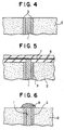
- Fig. 4 is a schematic cross-sectional view showing a via-structure formed in a multilayer interconnection ceramic substrate according to a first embodiment of the present invention.
- the multilayer interconnection substrate has a ceramic substrate 2, a via-conductor 1 penetrating the ceramic substrate 2 and a resin layer 3 formed at the interface of the via-conductor 1 and the ceramic substrate 2.
- the gap, between the via-conductor and the ceramic is provided by controlling an ambient atmosphere for sintering and by controlling a composition in a paste
- the method for providing the gap is not limited to any of those. It is preferable that thermosetting resins to be cured at a temperature between 300 and 500°C, such as polyimide or benzo-cyclo-butene, are employed in the present invention.
- the compositions of the resins are, however, not limited to any of those, but extended to wide varieties of materials. Materials for the substrate and for the conductor are not limited, either.
- substantially no crack is formed in ceramic substrates because the gap is formed and present during a sintering step at the interface between the via-conductor and the ceramic substrate.
- the resin layer is formed in the gap between the via-conductor and the ceramic substrate. Flexibility of tile resin layer can prevent a crack in the ceramic substrate, which would generate in the vicinity of the via-conductor during successive steps because of a difference in thermal expansion coefficient.
- the electric reliability can be improved because the resin layer prevents moisture and others from intrusion.
- failures such as swelling of the resin can be avoided because no crack is generated in the ceramic substrate and the gap is filled with the resin.
- Figs. 5 and 6 each shows a multilayer interconnection substrate according to another embodiment.
- the multilayer interconnection substrate of Fig.5 has a polyimide layer 6 for receiving an interconnection layer 7 and formed on the surface of a ceramic substrate 2.
- the interconnection layer 7 is connected to the via-conductor 1.
- the multilayer interconnection substrate of Fig. 6 has a terminal 8 on the surface of a ceramic substrate 2.
- the terminal 8 is connected to a via-conductor 1 surrounded by a resin layer 3.
- Embodiments 1 to 5 wherein a variety of materials are employed for a substrate, a via-conductor and a resin film and a variety of conditions in ambient atmosphere and temperature for sintering and curing.
- a multilayer interconnection ceramic substrate having a specific permittivity of 7.1 and including a via-conductor made of Ag and a glass-ceramic substrate composed of boro-silicate glass and alumina was formed by sintering in an N2-ambient at 900°C.
- a gap was generated at an interface between a via-conductor 1 and the substrate 2 while no crack was formed in the substrate.
- the resultant substrate was immersed into a polyimide precursor liquid and an ambient atmosphere was evacuated in vacuo . After removal of the substrate from the polyimide precursor liquid, the substrate was subjected to a curing step performed in a nitrogen gas stream at 450°C.
- the PCT result was such that, a terminal pattern is further formed on the substrate surface by employing sputtering and plating technologies. Then, a polyimide layer was formed by spin-coating on the substrate and hardened thermally. The process did not involve any irregularity such as swelling, resulting in formation of an excellent resin layer for multilayer interconnection.
- a multilayer interconnection ceramic substrate similar to Embodiment 1 and having a gap at an interface between a via-conductor 1 and the substrate 2 was formed and immersed in a benzo-cyclo-butene precursor liquid and the ambient atmosphere was evacuated in vacuo .
- the substrate was subjected to curing in a nitrogen gas stream at 300°C after removal from the benzo-cyclo-butene precursor liquid.
- An SEM observation performed both on the substrate surface and a cross-sectional surface of the substrate after mechanical polishing of the substrate surface clarified that a resin layer was formed perfectly between the via-conductor 1 and the ceramic substrate 2 and from the surface to a depth of about 0.5 mm in the gap, as shown in Fig. 4.
- an ink impregnation test performed on the resultant substrate indicated that any ink impregnation was not observed.
- a PCT applied to the substrate after sputter-deposition of an interconnection pattern on the substrate surface did not detect any irregularity even after 1000 hours.
- a step for hardening the benzo-cyclo-butene precursor layer spin-coated on the substrate after formation of a terminal pattern on the substrate surface by employing sputtering and plating technologies did not induce any irregularity such as swelling, resulting in formation of an excellent resin layer for multilayer interconnection.
- a multilayer interconnection ceramic substrate having a specific permittivity of 6.0 and including a via-conductor made of Cu and a glass-ceramic substrate composed of boro-silicate glass and alumina was formed by sintering in an N2-ambient at 950°C.
- a gap was formed at an interface between a via-conductor 1 and the substrate 2 while no crack was generated in the substrate.
- An ambient atmosphere was evacuated in vacuo during immersion of the resultant substrate into a polyimide precursor liquid. After removal of the substrate from the polyimide precursor liquid, the substrate was subjected to curing in a nitrogen gas stream at 450°C.
- a multilayer interconnection ceramic substrate similar to Embodiment 3 and having a gap at an interface between a via-conductor 1 and the substrate 2 was formed and immersed into a benzo-cyclo-butene precursor liquid and the ambient atmosphere was evacuated in vacuo . After removal from the benzo-cyclo-butene precursor liquid, the substrate was subjected to curing in a nitrogen gas stream at 300°C. An SEM observation of the substrate surface and a cross-sectional surface after mechanical polishing of the substrate surface clarified that a resin layer was formed perfectly between the via-conductor 1 and the ceramic substrate 2 and from the surface to a depth of about 0.5 mm in the gap, as shown in Fig. 4.
- an ink impregnation test performed on the resultant substrate did not detect any impregnation.
- a PCT applied to the substrate after formation of an interconnection pattern on the substrate surface by employing a sputter-deposition technology did not exhibit any irregularity even after 1000 hours.
- Hardening a benzo-cyclo-butene precursor layer spin-coated on the substrate after formation of a terminal pattern on the substrate surface by employing sputtering and plating technologies did not provide any irregularity such as swelling, resulting in formation of an excellent resin layer for multilayer interconnection.
- a multilayer interconnection ceramic substrate having a specific permittivity of 4.4 and including a via-conductor made of Ag and a glass-ceramic substrate composed of boro-silicate glass, quartz glass and cordierite was formed by sintering in an N2-ambient at 900°C.
- a gap was generated at an interface between a via-conductor 1 and the substrate 2 while no crack was generated in the ceramic substrate.
- the resultant substrate was immersed into a polyimide precursor liquid and the ambient atmosphere was evacuated in vacuo . After removal of the substrate from the polyimide precursor liquid, the substrate was subjected to curing in a nitrogen gas stream at 450°C.
- a benzo-cyclo-butene precursor layer was spin-coated on the substrate and hardened after formation of a terminal pattern on the substrate surface by employing sputtering and plating technologies did not provide any irregularity such as swelling, resulting in formation of an excellent resin layer for multilayer interconnection.
- a multilayer interconnection ceramic substrate similar to Embodiment 5 and having a gap at an interface between a via-conductor 1 and the substrate 2 was formed and immersed into a benzo-cyclo-butene precursor liquid and an ambient atmosphere was evacuated in vacuo .
- the substrate was subjected to curing in a nitrogen gas stream at 300°C after removal from the benzo-cyclo-butene precursor liquid.
- An SEM observation performed on the substrate surface and a cross-sectional surface after mechanical polishing of the substrate surface clarified that a resin layer was formed perfectly between the via-conductor 1 and the ceramic substrate 2 and from the surface to a depth of about 0.5 mm in the gap, as shown in Fig. 4.
- an ink impregnation test performed on the resultant substrate surface did not detect any impregnation.
- a PCT applied to the substrate after formation of an interconnection pattern on the substrate surface by employing a sputter-deposition technology did not exhibit any irregularity after 1000 hours.
- Hardening a benzo-cyclo-butene layer spin-coated on the substrate after formation of a terminal pattern on the substrate surface by employing sputtering and plating technologies did not provide any irregularity such as swelling, resulting in formation of an excellent resin layer for multilayer interconnection.
- a multilayer interconnection ceramic substrate having a specific permittivity of 7.1 and including a via-conductor made of Ag and a glass-ceramic substrate composed of boro-silicate glass and alumina was formed by sintering in an open-air at 900°C. It was observed that cracks had generated in a portion of the substrate adjacent to a via-conductor.
- a step for hardening a polyimide layer spin-coated on the substrate thus formed after formation of a terminal pattern on the substrate surface by employing sputtering and plating technologies induced an irregularity of swelling.
- I/O pins which were welded onto the resultant substrate by employing an Au-Sn solder, fractured the substrate when a lateral strain was applied to the I/O pins.
- a multilayer interconnection ceramic substrate having a specific permittivity of 7.1 and including a via-conductor made of silver and a glass-ceramic substrate composed of boro-silicate glass and alumina was formed by sintering in an N2-ambient at 900°C. it was observed that a gap had generated at an interface between a via-conductor 1 and the substrate 2.
- a PCT applied to the resultant substrate after formation of an interconnection pattern by employing a sputter-deposition technology indicated a corrosion-induced rise in resistance of the conductor after only 100 hours elapsed.
- Hardening a polyimide layer spin-coated on the substrate after formation of a terminal pattern on the substrate surface by employing sputtering and plating technologies generated an irregularity of swelling.
- a pattern was formed by employing sputtering and plating technologies on a surface of a multilayer interconnection ceramic substrate having cracks similar to Comparative Example 1.
- a step for hardening a benzo-cyclo-butene layer spin-coated on the resultant substrate induced an irregularity of swelling.
- a pattern was formed by employing sputtering and plating technologies on & multilayer interconnection ceramic substrate having a gap at an interface between a via-conductor and the substrate similarly to Comparative Example 2.
- a step for hardening a benzo-cyclo-butene layer coated on the resultant substrate induced an irregularity of swelling.
- the present invention can provide a multilayer interconnection ceramic substrate having a high reliability and a high strength, which can be produced at a low cost.
- a structure enforced in the vicinity of a via-conductor in a multilayer interconnection ceramic substrate, such as an insulating substrate, a multi-chip module substrate and a semiconductor package, according to the present invention is useful as a bonded structure in a semiconductor device for mounting LSI chips and packagings, which has an extremely high industrial value.
Abstract
Description
- The present invention relates to a via-structure of a multilayer interconnection ceramic substrate and, more particularly, to an enforced via-structure of a low cost ceramic substrate for mounting LSI chips and packagings.
- Multilayer interconnection ceramic substrates including, for examples, an insulating substrate, multilayer printed circuit board and ceramic packages for mounting LSIs are used in a large amount in the semiconductor industry.
- Figs. 1 and 2 are partial cross-sectional views each for showing a problem in a conventional multilayer interconnection ceramic substrate having a via-conductor formed in the vicinity of the substrate surface. In general, a via-conductor of a multilayer interconnection ceramic substrate, which interconnects terminals or bonding posts for inner leads, outer leads, semiconductor chips and packagings, is composed of a metal or an alloy such as W, Mo, Au, Ag, Cu or Ag-Pd. Since a metal has a thermal expansion coefficient higher than that of ceramic, cracks 4 shown in Fig. 1 frequently appear during steps for sintering and for post-treatment. Although adhesive force of the ceramics to the via-conductor may be reduced in order to eliminate the cracks 4 in Fig. 1 by controlling a composition in a paste or an atmosphere for sintering, a peeling-off shown in Fig. 2 will arises instead due to the low adhesive force. Hence, conventional multilayer interconnection ceramic substrates suffer problems of a low mechanical strength and a low reliability in electric performance.
- Recently, a multilayer interconnection substrate composed of a ceramic substrate is reported, which has a polyimide layer for interconnection layers and is formed on the ceramic substrate. The ceramic substrate, however, will have cracks in the vicinity of the substrate surface as shown in Fig. 3. In view of the problem of the cracks, another ceramic substrate is proposed, which has thereon a photo-sensitive resin film for covering cracks and having holes only for through-holes, by Patent Publication No. JP-A-90-234456. However, a photo-sensitive resin film has a problem that a manufacturing cost for a semiconductor devices rises high and an additional problem that cracks and peeling-offs formed in the ceramic substrate involve failures such as swelling of the resin.
- Meanwhile, it is proposed by Patent Publication No. JP-A-91-145796 that, in a printed circuit board having a through-hole filled with a conductive paste, treatment of a sidewall surface of the through-hole with a silane coupling agent strengthens an affinity between a conductive paste and an insulator layer formed by impregnating a resin into a base material having a sheet form. However, such a treatment cannot eliminate any cracks when it is applied to a sintered metallic conductor and a ceramic insulator.
- As a countermeasure to a metallic ion migration, a method for manufacturing a printed circuit board is proposed by Patent Publication No. JP-A-91-91992, wherein a through-hole is filled with an insulating resin and a conductive paste. This technology, however, cannot be applied if the substrate is of ceramics or if the conductor is of a sintered metal.
- As described above, it is difficult to obtain a structure having a high strength and a high electric reliability at a low cost in a multilayer interconnection ceramic substrate having a via-hole.
- In view of the foregoing, it is an object of the present invention to provide a multilayer interconnection ceramic substrate having a high strength and a high electric reliability manufactured at a low cost.
- According to the present invention, there is provided a multilayer interconnection substrate comprising a ceramic substrate, a via-conductor penetrating the ceramic substrate, a resin layer formed at an interface between the via-conductor and the ceramic substrate and at least in the vicinity of the surface of the ceramic substrate.
- The above and further objects as well as features and advantages of the present invention will be more apparent from the following description, taken in conjunction with the accompanying drawings in which:
- Fig. 1 is a cross-sectional view showing a conventional multilayer interconnection ceramic substrate having cracks in the vicinity of a via-conductor;
- Fig. 2 is a cross-sectional view showing a conventional multilayer interconnection ceramic substrate having a peeling-off in the vicinity of a via-conductor;
- Fig. 3 is a cross-sectional view showing a conventional multilayer interconnection ceramic substrate having a polyimide layer for multilayer interconnection;
- Fig. 4 is a cross-sectional view showing an enforced structure in the vicinity of a via-conductor in a multilayer interconnection ceramic substrate according to an embodiment of the the present invention; and
- Figs. 5 and 6 are cross-sectional views each showing an enforced structure in the vicinity of a via-conductor in a multilayer interconnection ceramic substrate according to another embodiment of the the present invention.
- Now, preferred embodiments will be described with reference to the drawings. Fig. 4 is a schematic cross-sectional view showing a via-structure formed in a multilayer interconnection ceramic substrate according to a first embodiment of the present invention. The multilayer interconnection substrate has a
ceramic substrate 2, a via-conductor 1 penetrating theceramic substrate 2 and aresin layer 3 formed at the interface of the via-conductor 1 and theceramic substrate 2. - Although it is preferable that the gap, between the via-conductor and the ceramic is provided by controlling an ambient atmosphere for sintering and by controlling a composition in a paste, the method for providing the gap is not limited to any of those. It is preferable that thermosetting resins to be cured at a temperature between 300 and 500°C, such as polyimide or benzo-cyclo-butene, are employed in the present invention. The compositions of the resins are, however, not limited to any of those, but extended to wide varieties of materials. Materials for the substrate and for the conductor are not limited, either.
- In the present invention, substantially no crack is formed in ceramic substrates because the gap is formed and present during a sintering step at the interface between the via-conductor and the ceramic substrate. After the sintering step, the resin layer is formed in the gap between the via-conductor and the ceramic substrate. Flexibility of tile resin layer can prevent a crack in the ceramic substrate, which would generate in the vicinity of the via-conductor during successive steps because of a difference in thermal expansion coefficient. On the other hand, the electric reliability can be improved because the resin layer prevents moisture and others from intrusion. Furthermore, failures such as swelling of the resin can be avoided because no crack is generated in the ceramic substrate and the gap is filled with the resin.
- Figs. 5 and 6 each shows a multilayer interconnection substrate according to another embodiment. The multilayer interconnection substrate of Fig.5 has a polyimide layer 6 for receiving an
interconnection layer 7 and formed on the surface of aceramic substrate 2. Theinterconnection layer 7 is connected to the via-conductor 1. - The multilayer interconnection substrate of Fig. 6 has a terminal 8 on the surface of a
ceramic substrate 2. The terminal 8 is connected to a via-conductor 1 surrounded by aresin layer 3. - Hereinafter, examples of embodiments will be described as
Embodiments 1 to 5 wherein a variety of materials are employed for a substrate, a via-conductor and a resin film and a variety of conditions in ambient atmosphere and temperature for sintering and curing. - A multilayer interconnection ceramic substrate having a specific permittivity of 7.1 and including a via-conductor made of Ag and a glass-ceramic substrate composed of boro-silicate glass and alumina was formed by sintering in an N₂-ambient at 900°C. A gap was generated at an interface between a via-
conductor 1 and thesubstrate 2 while no crack was formed in the substrate. The resultant substrate was immersed into a polyimide precursor liquid and an ambient atmosphere was evacuated in vacuo. After removal of the substrate from the polyimide precursor liquid, the substrate was subjected to a curing step performed in a nitrogen gas stream at 450°C. - An SEM (Scanning Electron Microscopic) observation performed on the substrate surface and a cross-sectional surface of the substrate after mechanical polishing of the substrate surface clarified that a resin layer was formed perfectly between the via-conductor and the substrate and from the surfaces to a depth of about 0.5 mm in the gap, as shown in Fig. 4. Furthermore, an ink impregnation test performed on the substrate thus obtained indicated that no impregnation took place at all. Moreover, a PCT (Pressure Cooker Test) applied to the substrate after formation of an interconnection pattern by sputter-deposition on the substrate surface did not detect any irregularity after 1000 hours elapsed. The PCT result was such that, a terminal pattern is further formed on the substrate surface by employing sputtering and plating technologies. Then, a polyimide layer was formed by spin-coating on the substrate and hardened thermally. The process did not involve any irregularity such as swelling, resulting in formation of an excellent resin layer for multilayer interconnection.
- A multilayer interconnection ceramic substrate similar to
Embodiment 1 and having a gap at an interface between a via-conductor 1 and thesubstrate 2 was formed and immersed in a benzo-cyclo-butene precursor liquid and the ambient atmosphere was evacuated in vacuo. The substrate was subjected to curing in a nitrogen gas stream at 300°C after removal from the benzo-cyclo-butene precursor liquid. An SEM observation performed both on the substrate surface and a cross-sectional surface of the substrate after mechanical polishing of the substrate surface clarified that a resin layer was formed perfectly between the via-conductor 1 and theceramic substrate 2 and from the surface to a depth of about 0.5 mm in the gap, as shown in Fig. 4. - Furthermore, an ink impregnation test performed on the resultant substrate indicated that any ink impregnation was not observed. Moreover, a PCT applied to the substrate after sputter-deposition of an interconnection pattern on the substrate surface did not detect any irregularity even after 1000 hours. A step for hardening the benzo-cyclo-butene precursor layer spin-coated on the substrate after formation of a terminal pattern on the substrate surface by employing sputtering and plating technologies did not induce any irregularity such as swelling, resulting in formation of an excellent resin layer for multilayer interconnection.
- A multilayer interconnection ceramic substrate having a specific permittivity of 6.0 and including a via-conductor made of Cu and a glass-ceramic substrate composed of boro-silicate glass and alumina was formed by sintering in an N₂-ambient at 950°C. A gap was formed at an interface between a via-
conductor 1 and thesubstrate 2 while no crack was generated in the substrate. An ambient atmosphere was evacuated in vacuo during immersion of the resultant substrate into a polyimide precursor liquid. After removal of the substrate from the polyimide precursor liquid, the substrate was subjected to curing in a nitrogen gas stream at 450°C. - An SEM observation performed on the substrate surface and a cross-sectional surface after mechanical polishing of the substrate surface detected that a resin layer was formed perfectly between the via-
conductor 1 and theceramic substrate 2 and from the surface to a depth of about 0.5 mm in the gap, as shown in Fig. 4. An ink impregnation test performed on the resultant substrate did not detect any impregnation. Moreover, a PCT applied to the substrate after formation of an interconnection pattern on the substrate surface by employing a sputter-deposition technology did not detect any irregularity even after 1000 hours. Furthermore, hardening the polyimide precursor layer coated on the substrate after formation of a terminal pattern on the substrate surface, by employing sputtering and plating technologies did not provided any irregularity such as swelling, resulting in formation of an excellent resin layer for multilayer interconnection. - A multilayer interconnection ceramic substrate similar to
Embodiment 3 and having a gap at an interface between a via-conductor 1 and thesubstrate 2 was formed and immersed into a benzo-cyclo-butene precursor liquid and the ambient atmosphere was evacuated in vacuo. After removal from the benzo-cyclo-butene precursor liquid, the substrate was subjected to curing in a nitrogen gas stream at 300°C. An SEM observation of the substrate surface and a cross-sectional surface after mechanical polishing of the substrate surface clarified that a resin layer was formed perfectly between the via-conductor 1 and theceramic substrate 2 and from the surface to a depth of about 0.5 mm in the gap, as shown in Fig. 4. - Furthermore, an ink impregnation test performed on the resultant substrate did not detect any impregnation. A PCT applied to the substrate after formation of an interconnection pattern on the substrate surface by employing a sputter-deposition technology did not exhibit any irregularity even after 1000 hours. Hardening a benzo-cyclo-butene precursor layer spin-coated on the substrate after formation of a terminal pattern on the substrate surface by employing sputtering and plating technologies did not provide any irregularity such as swelling, resulting in formation of an excellent resin layer for multilayer interconnection.
- A multilayer interconnection ceramic substrate having a specific permittivity of 4.4 and including a via-conductor made of Ag and a glass-ceramic substrate composed of boro-silicate glass, quartz glass and cordierite was formed by sintering in an N₂-ambient at 900°C. A gap was generated at an interface between a via-
conductor 1 and thesubstrate 2 while no crack was generated in the ceramic substrate. The resultant substrate was immersed into a polyimide precursor liquid and the ambient atmosphere was evacuated in vacuo. After removal of the substrate from the polyimide precursor liquid, the substrate was subjected to curing in a nitrogen gas stream at 450°C. - An SEM observation performed on the substrate surface and a cross-sectional surface after mechanical polishing of the substrate surface clarified that a resin layer was formed perfectly between the via-
conductor 1 and theceramic substrate 2 and from the substrate surface to a depth of about 0.5 mm in the gap, as shown in Fig. 4. Moreover, an ink impregnation test performed on the resultant substrate did not detect any impregnation. A PCT applied to the substrate after formation of an interconnection pattern on the substrate surface by employing a sputter-deposition technology did not exhibit any irregularity even when 1000 hours elapsed. A benzo-cyclo-butene precursor layer was spin-coated on the substrate and hardened after formation of a terminal pattern on the substrate surface by employing sputtering and plating technologies did not provide any irregularity such as swelling, resulting in formation of an excellent resin layer for multilayer interconnection. - A multilayer interconnection ceramic substrate similar to Embodiment 5 and having a gap at an interface between a via-
conductor 1 and thesubstrate 2 was formed and immersed into a benzo-cyclo-butene precursor liquid and an ambient atmosphere was evacuated in vacuo. The substrate was subjected to curing in a nitrogen gas stream at 300°C after removal from the benzo-cyclo-butene precursor liquid. An SEM observation performed on the substrate surface and a cross-sectional surface after mechanical polishing of the substrate surface clarified that a resin layer was formed perfectly between the via-conductor 1 and theceramic substrate 2 and from the surface to a depth of about 0.5 mm in the gap, as shown in Fig. 4. - Moreover, an ink impregnation test performed on the resultant substrate surface did not detect any impregnation. A PCT applied to the substrate after formation of an interconnection pattern on the substrate surface by employing a sputter-deposition technology did not exhibit any irregularity after 1000 hours. Hardening a benzo-cyclo-butene layer spin-coated on the substrate after formation of a terminal pattern on the substrate surface by employing sputtering and plating technologies did not provide any irregularity such as swelling, resulting in formation of an excellent resin layer for multilayer interconnection.
- A multilayer interconnection ceramic substrate having a specific permittivity of 7.1 and including a via-conductor made of Ag and a glass-ceramic substrate composed of boro-silicate glass and alumina was formed by sintering in an open-air at 900°C. It was observed that cracks had generated in a portion of the substrate adjacent to a via-conductor. A step for hardening a polyimide layer spin-coated on the substrate thus formed after formation of a terminal pattern on the substrate surface by employing sputtering and plating technologies induced an irregularity of swelling. Furthermore, I/O pins, which were welded onto the resultant substrate by employing an Au-Sn solder, fractured the substrate when a lateral strain was applied to the I/O pins.
- A multilayer interconnection ceramic substrate having a specific permittivity of 7.1 and including a via-conductor made of silver and a glass-ceramic substrate composed of boro-silicate glass and alumina was formed by sintering in an N₂-ambient at 900°C. it was observed that a gap had generated at an interface between a via-
conductor 1 and thesubstrate 2. A PCT applied to the resultant substrate after formation of an interconnection pattern by employing a sputter-deposition technology indicated a corrosion-induced rise in resistance of the conductor after only 100 hours elapsed. Hardening a polyimide layer spin-coated on the substrate after formation of a terminal pattern on the substrate surface by employing sputtering and plating technologies generated an irregularity of swelling. - A pattern was formed by employing sputtering and plating technologies on a surface of a multilayer interconnection ceramic substrate having cracks similar to Comparative Example 1. A step for hardening a benzo-cyclo-butene layer spin-coated on the resultant substrate induced an irregularity of swelling. I/O pins welded to this substrate by employing an Au-Sn solder fractured the substrate when a lateral strain was applied to the I/O pins.
- A pattern was formed by employing sputtering and plating technologies on & multilayer interconnection ceramic substrate having a gap at an interface between a via-conductor and the substrate similarly to Comparative Example 2. A step for hardening a benzo-cyclo-butene layer coated on the resultant substrate induced an irregularity of swelling.
- As described above, the present invention can provide a multilayer interconnection ceramic substrate having a high reliability and a high strength, which can be produced at a low cost.
- A structure enforced in the vicinity of a via-conductor in a multilayer interconnection ceramic substrate, such as an insulating substrate, a multi-chip module substrate and a semiconductor package, according to the present invention is useful as a bonded structure in a semiconductor device for mounting LSI chips and packagings, which has an extremely high industrial value.
- Although the present invention is described with reference to the preferred embodiments, the present invention is not limited to such embodiments and it will be obvious for those skilled in the art that various modifications or alterations can be easily made based on the above embodiments within the scope of the present invention.
Claims (9)
- A multilayer interconnection substrate comprising a ceramic substrate (2), a via conductor (1) penetrating said ceramic substrate (2), a resin layer (3) formed at an interface between said via-conductor (1) and said ceramic substrate (2) at least in the vicinity of the surface of said ceramic substrate (2).
- A multilayer interconnection substrate as defined in Claim 1 further comprising a polyimide layer (6), formed on said ceramic substrate (2), for receiving an interconnection substrate (7) connected to said via-conductor (1).
- A multilayer interconnection substrate as defined in Claim 1 further comprising a terminal overlying said ceramic layer (2) and connected to said via-conductor (1).
- A multilayer interconnection substrate as defined, in one of Claims 1 to 3 wherein said resin layer (3) is made of a resin selected from a group consisting of polyimide and benzo-cyclo-butene.
- A multilayer interconnection substrate as defined in one of Claims 1 to 3 wherein said resin layer (3) is made of a thermo-setting resin.
- A multilayer interconnection substrate as defined in one of Claims 1 to 3 wherein said via-conductor (1) is made of a material selected from a group consisting of W, Mo, Au, Ag, Cu and Ag-Pd.
- A method for manufacturing a multilayer interconnection substrate including consecutive steps of sintering a ceramic substrate (2) and a via-conductor (1) penetrating therethrough, and immersing said ceramic substrate in a resin solution or resin precursor solution to form a resin layer (3) in a gap between said ceramic substrate (2) and said via conductor (1) at least in the vicinity of the surface of said ceramic substrate (2).
- A method for manufacturing a multilayer interconnection substrate as defined in Claim 7 wherein said sintering is effected in a nitrogen ambient at a temperature ranging from 850 to 1000 °C .
- A method for manufacturing a multilayer interconnection substrate as defined in Claim 7 or 8 wherein said curing is effected in a nitrogen ambient at a temperature ranging from 300 to 500 °C .
Applications Claiming Priority (2)
| Application Number | Priority Date | Filing Date | Title |
|---|---|---|---|
| JP99817/94 | 1994-05-13 | ||
| JP6099817A JP2570617B2 (en) | 1994-05-13 | 1994-05-13 | Via structure of multilayer wiring ceramic substrate and method of manufacturing the same |
Publications (2)
| Publication Number | Publication Date |
|---|---|
| EP0682363A2 true EP0682363A2 (en) | 1995-11-15 |
| EP0682363A3 EP0682363A3 (en) | 1997-05-14 |
Family
ID=14257401
Family Applications (1)
| Application Number | Title | Priority Date | Filing Date |
|---|---|---|---|
| EP95107251A Withdrawn EP0682363A3 (en) | 1994-05-13 | 1995-05-12 | Via-structure of a multilayer interconnection ceramic substrate. |
Country Status (3)
| Country | Link |
|---|---|
| US (1) | US5576518A (en) |
| EP (1) | EP0682363A3 (en) |
| JP (1) | JP2570617B2 (en) |
Cited By (2)
| Publication number | Priority date | Publication date | Assignee | Title |
|---|---|---|---|---|
| EP0926931A1 (en) * | 1997-04-16 | 1999-06-30 | Shinko Electric Industries Co. Ltd. | Wiring board having vias |
| WO2004064466A1 (en) * | 2003-01-14 | 2004-07-29 | Matsushita Electric Industrial Co., Ltd. | High-frequency layered part and manufacturing method thereof |
Families Citing this family (17)
| Publication number | Priority date | Publication date | Assignee | Title |
|---|---|---|---|---|
| US6195883B1 (en) * | 1998-03-25 | 2001-03-06 | International Business Machines Corporation | Full additive process with filled plated through holes |
| US6291779B1 (en) * | 1999-06-30 | 2001-09-18 | International Business Machines Corporation | Fine pitch circuitization with filled plated through holes |
| DE60031448T2 (en) * | 2000-01-13 | 2007-02-01 | Nitto Denko Corp., Ibaraki | POROUS ADHESIVE FOIL, SEMICONDUCTOR WAIST WITH POROUS ADHESIVE FOIL AND METHOD FOR THE PRODUCTION THEREOF |
| US6465085B1 (en) * | 2000-04-04 | 2002-10-15 | Fujitsu Limited | Thin film wiring board and method for manufacturing the same, base substrate and method for manufacturing the same |
| DE10150715A1 (en) * | 2001-10-13 | 2003-04-30 | Bosch Gmbh Robert | Green ceramic insert body, ceramic insert body, ceramic green body or composite body and the ceramic layer composite produced therewith |
| US6770822B2 (en) * | 2002-02-22 | 2004-08-03 | Bridgewave Communications, Inc. | High frequency device packages and methods |
| US20050248002A1 (en) * | 2004-05-07 | 2005-11-10 | Michael Newman | Fill for large volume vias |
| US7205486B2 (en) * | 2004-07-16 | 2007-04-17 | Cardiac Pacemakers, Inc. | Thermally isolated via structure |
| JP2006302972A (en) * | 2005-04-15 | 2006-11-02 | Alps Electric Co Ltd | Wiring board and manufacturing method thereof |
| US7470863B2 (en) * | 2006-01-24 | 2008-12-30 | International Business Machines Corporation | Microelectronic device with mixed dielectric |
| US8581113B2 (en) | 2007-12-19 | 2013-11-12 | Bridgewave Communications, Inc. | Low cost high frequency device package and methods |
| KR100997989B1 (en) * | 2008-08-28 | 2010-12-03 | 삼성전기주식회사 | Multilayer ceramic substrate |
| KR100968977B1 (en) * | 2008-10-17 | 2010-07-14 | 삼성전기주식회사 | Non-shiringkage ceramic substrate and manufacturing method thereof |
| JP5330863B2 (en) * | 2009-03-04 | 2013-10-30 | パナソニック株式会社 | Manufacturing method of semiconductor device |
| KR101153492B1 (en) * | 2010-08-24 | 2012-06-11 | 삼성전기주식회사 | Manufacturing method for ceramic substrate for probe card and ceramic substrate for probe card |
| US9523715B2 (en) * | 2012-04-13 | 2016-12-20 | Formfactor, Inc. | Wiring substrate with filled vias to accommodate custom terminals |
| CN105628707B (en) * | 2015-12-30 | 2018-05-08 | 中电环保股份有限公司 | Water process resin boundary surface image-recognizing method |
Citations (2)
| Publication number | Priority date | Publication date | Assignee | Title |
|---|---|---|---|---|
| JPH0391992A (en) | 1989-09-04 | 1991-04-17 | Sharp Corp | Manufacture of printed wiring board |
| JPH03145796A (en) | 1989-10-31 | 1991-06-20 | Shin Kobe Electric Mach Co Ltd | Manufacture of through-hole printed wiring board |
Family Cites Families (17)
| Publication number | Priority date | Publication date | Assignee | Title |
|---|---|---|---|---|
| US3873756A (en) * | 1971-02-10 | 1975-03-25 | Gridcraft Inc | Insulating lining for metallic circuit board terminal holes |
| US4234367A (en) * | 1979-03-23 | 1980-11-18 | International Business Machines Corporation | Method of making multilayered glass-ceramic structures having an internal distribution of copper-based conductors |
| US4318954A (en) * | 1981-02-09 | 1982-03-09 | Boeing Aerospace Company | Printed wiring board substrates for ceramic chip carriers |
| JPS59193095A (en) * | 1983-04-15 | 1984-11-01 | 株式会社日立製作所 | Ceramic circuit board and its producing method |
| JPS61229389A (en) * | 1985-04-03 | 1986-10-13 | イビデン株式会社 | Ceramic wiring plate and manufacture thereof |
| US4740414A (en) * | 1986-11-17 | 1988-04-26 | Rockwell International Corporation | Ceramic/organic multilayer interconnection board |
| US4721831A (en) * | 1987-01-28 | 1988-01-26 | Unisys Corporation | Module for packaging and electrically interconnecting integrated circuit chips on a porous substrate, and method of fabricating same |
| US4880684A (en) * | 1988-03-11 | 1989-11-14 | International Business Machines Corporation | Sealing and stress relief layers and use thereof |
| JPH02234456A (en) * | 1989-03-08 | 1990-09-17 | Ngk Spark Plug Co Ltd | Integrated circuit package and manufacture thereof |
| JPH034592A (en) * | 1989-06-01 | 1991-01-10 | Fujitsu Ltd | Manufacture of ceramic board |
| JPH03138806A (en) * | 1989-10-24 | 1991-06-13 | Narumi China Corp | Conductive paste for filling and multi-layer wiring substrate |
| JPH03150894A (en) * | 1989-11-07 | 1991-06-27 | Fujitsu Ltd | Managing method for film thickness of multilayer thin film circuit board |
| US5121299A (en) * | 1989-12-29 | 1992-06-09 | International Business Machines Corporation | Multi-level circuit structure utilizing conductive cores having conductive protrusions and cavities therein |
| JPH04283993A (en) * | 1991-03-12 | 1992-10-08 | Fujitsu Ltd | Manufacture of thin-film multilayer substrate |
| JP3098288B2 (en) * | 1991-08-08 | 2000-10-16 | 株式会社デンソー | Conductor composition and ceramic substrate using the same |
| JPH0620516A (en) * | 1992-07-02 | 1994-01-28 | Nippondenso Co Ltd | Conductive composition, ceramic multilayered substrate and semiconductor device |
| JPH06104575A (en) * | 1992-09-22 | 1994-04-15 | Sumitomo Kinzoku Ceramics:Kk | Ceramic circuit board provided with resistor |
-
1994
- 1994-05-13 JP JP6099817A patent/JP2570617B2/en not_active Expired - Lifetime
-
1995
- 1995-05-12 EP EP95107251A patent/EP0682363A3/en not_active Withdrawn
- 1995-05-12 US US08/439,945 patent/US5576518A/en not_active Expired - Fee Related
Patent Citations (2)
| Publication number | Priority date | Publication date | Assignee | Title |
|---|---|---|---|---|
| JPH0391992A (en) | 1989-09-04 | 1991-04-17 | Sharp Corp | Manufacture of printed wiring board |
| JPH03145796A (en) | 1989-10-31 | 1991-06-20 | Shin Kobe Electric Mach Co Ltd | Manufacture of through-hole printed wiring board |
Cited By (4)
| Publication number | Priority date | Publication date | Assignee | Title |
|---|---|---|---|---|
| EP0926931A1 (en) * | 1997-04-16 | 1999-06-30 | Shinko Electric Industries Co. Ltd. | Wiring board having vias |
| EP0926931A4 (en) * | 1997-04-16 | 2006-12-06 | Shinko Electric Ind Co | Wiring board having vias |
| WO2004064466A1 (en) * | 2003-01-14 | 2004-07-29 | Matsushita Electric Industrial Co., Ltd. | High-frequency layered part and manufacturing method thereof |
| US7297878B2 (en) | 2003-01-14 | 2007-11-20 | Matsushita Electric Industrial Co., Ltd. | High frequency laminated component and its manufacturing method |
Also Published As
| Publication number | Publication date |
|---|---|
| JPH07307573A (en) | 1995-11-21 |
| EP0682363A3 (en) | 1997-05-14 |
| US5576518A (en) | 1996-11-19 |
| JP2570617B2 (en) | 1997-01-08 |
Similar Documents
| Publication | Publication Date | Title |
|---|---|---|
| US5576518A (en) | Via-structure of a multilayer interconnection ceramic substrate | |
| US7820916B2 (en) | Composite ceramic substrate | |
| US5677575A (en) | Semiconductor package having semiconductor chip mounted on board in face-down relation | |
| US5549778A (en) | Manufacturing method for multilayer ceramic substrate | |
| US20050000725A1 (en) | Manufacturing method for a printed circuit board | |
| CN1290424A (en) | Encapsulated surface wave component and collective method for making same | |
| US6933448B2 (en) | Printed circuit board having permanent solder mask | |
| US5760466A (en) | Semiconductor device having improved heat resistance | |
| US6218736B1 (en) | Circuit board and semiconductor device, and method of manufacturing the same | |
| JP3199637B2 (en) | Method for manufacturing multilayer wiring board | |
| JP3085649B2 (en) | Transfer sheet and method of manufacturing wiring board using the same | |
| JP3071764B2 (en) | Film with metal foil and method of manufacturing wiring board using the same | |
| JP3071723B2 (en) | Method for manufacturing multilayer wiring board | |
| JP3152852B2 (en) | Wiring board and manufacturing method thereof | |
| JP2000252391A (en) | Wiring board for mounting semiconductor device and its mounting structure | |
| JP3748283B2 (en) | Manufacturing method of laminated glass ceramic circuit board | |
| JP3758811B2 (en) | Transfer sheet and wiring board manufacturing method using the same | |
| JP3305574B2 (en) | Wiring board | |
| JP3659441B2 (en) | Wiring board | |
| JP3292623B2 (en) | Wiring board and method of manufacturing the same | |
| JP3502759B2 (en) | Semiconductor element mounting structure and wiring board mounting structure | |
| JP2676107B2 (en) | Substrate for mounting electronic components | |
| JP2002016176A (en) | Wiring board and connection structure therefor | |
| EP0354341B1 (en) | A composite structure for use in electronic packages | |
| JPH10322030A (en) | Multilayered wiring board |
Legal Events
| Date | Code | Title | Description |
|---|---|---|---|
| PUAI | Public reference made under article 153(3) epc to a published international application that has entered the european phase |
Free format text: ORIGINAL CODE: 0009012 |
|
| AK | Designated contracting states |
Kind code of ref document: A2 Designated state(s): DE FR GB |
|
| PUAL | Search report despatched |
Free format text: ORIGINAL CODE: 0009013 |
|
| AK | Designated contracting states |
Kind code of ref document: A3 Designated state(s): DE FR GB |
|
| 17P | Request for examination filed |
Effective date: 19970820 |
|
| 17Q | First examination report despatched |
Effective date: 19990330 |
|
| STAA | Information on the status of an ep patent application or granted ep patent |
Free format text: STATUS: THE APPLICATION IS DEEMED TO BE WITHDRAWN |
|
| 18D | Application deemed to be withdrawn |
Effective date: 19990810 |