EP0678907B1 - Method for fabricating reverse-staggered thin-film transistor - Google Patents
Method for fabricating reverse-staggered thin-film transistor Download PDFInfo
- Publication number
- EP0678907B1 EP0678907B1 EP95105936A EP95105936A EP0678907B1 EP 0678907 B1 EP0678907 B1 EP 0678907B1 EP 95105936 A EP95105936 A EP 95105936A EP 95105936 A EP95105936 A EP 95105936A EP 0678907 B1 EP0678907 B1 EP 0678907B1
- Authority
- EP
- European Patent Office
- Prior art keywords
- layer
- type
- amorphous silicon
- film transistor
- thin
- Prior art date
- Legal status (The legal status is an assumption and is not a legal conclusion. Google has not performed a legal analysis and makes no representation as to the accuracy of the status listed.)
- Expired - Lifetime
Links
Images

Classifications
-
- H—ELECTRICITY
- H10—SEMICONDUCTOR DEVICES; ELECTRIC SOLID-STATE DEVICES NOT OTHERWISE PROVIDED FOR
- H10D—INORGANIC ELECTRIC SEMICONDUCTOR DEVICES
- H10D30/00—Field-effect transistors [FET]
- H10D30/01—Manufacture or treatment
- H10D30/021—Manufacture or treatment of FETs having insulated gates [IGFET]
- H10D30/031—Manufacture or treatment of FETs having insulated gates [IGFET] of thin-film transistors [TFT]
- H10D30/0312—Manufacture or treatment of FETs having insulated gates [IGFET] of thin-film transistors [TFT] characterised by the gate electrodes
- H10D30/0316—Manufacture or treatment of FETs having insulated gates [IGFET] of thin-film transistors [TFT] characterised by the gate electrodes of lateral bottom-gate TFTs comprising only a single gate
-
- H10P10/00—
-
- H—ELECTRICITY
- H10—SEMICONDUCTOR DEVICES; ELECTRIC SOLID-STATE DEVICES NOT OTHERWISE PROVIDED FOR
- H10D—INORGANIC ELECTRIC SEMICONDUCTOR DEVICES
- H10D30/00—Field-effect transistors [FET]
- H10D30/01—Manufacture or treatment
- H10D30/021—Manufacture or treatment of FETs having insulated gates [IGFET]
- H10D30/031—Manufacture or treatment of FETs having insulated gates [IGFET] of thin-film transistors [TFT]
- H10D30/0321—Manufacture or treatment of FETs having insulated gates [IGFET] of thin-film transistors [TFT] comprising silicon, e.g. amorphous silicon or polysilicon
-
- H—ELECTRICITY
- H10—SEMICONDUCTOR DEVICES; ELECTRIC SOLID-STATE DEVICES NOT OTHERWISE PROVIDED FOR
- H10D—INORGANIC ELECTRIC SEMICONDUCTOR DEVICES
- H10D30/00—Field-effect transistors [FET]
- H10D30/60—Insulated-gate field-effect transistors [IGFET]
- H10D30/67—Thin-film transistors [TFT]
Definitions
- the present invention relates to a method for fabricating a thin-film transistor and, more particularly, to a method for fabricating a reverse-staggered thin-film transistor employed in a liquid crystal display device.
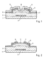
- Fig. 1 shows a conventional thin-film transistor of an amorphous silicon.
- This thin-film transistor is constituted by a gate electrode 2, a gate insulating film 3 made of a silicon nitride film, an intrinsic amorphous silicon layer 4 and an n-type amorphous silicon contact layer 5, a drain electrode 6 and a source electrode 7.
- a protective layer 9 made of silicon nitride is further formed to cover the transistor.
- the surface portion 10 of the amorphous silicon layer 4 between the drain electrode 6 and the source electrode 7 is sometimes called a "back channel" and has one of key factors determining the characteristics of the transistor.
- a leak current is caused to increase and thus flows between the source and drain. Even if the back channel 10 is not contaminated, the positive electric charges due to the contamination on the protective film 9 increase an electric field applied the back channel 10 up to or more than the threshold of the back channel. A leakage current thereby flows. Besides, the protective film 9 itself may be charged positively, so that the leak current also flows.
- such a thin-film transistor is disclosed in Japanese Patent Laid-Open No. Hei 2-163972 that a back channel covered with an oxide film obtained from hydrogen peroxide or with an alumina film formed by the CVD process. Such a film can convert the back channel into a p-type one. The leakage current is thereby decreased.
- the p-type back channel thus converted depends on the quality of the oxide or the alumina film and is thus inferior in controllability.
- the drain and source electrodes are damaged by the hydrogen peroxide.
- alumina in the alumina film may be diffused into the amorphous silicon layer to change the property of a thin-film transistor.
- FIG. 2 there are shown another thin-film transistor which is disclosed in Japanese Patent Publication No. Hei 5- 083197, in which the same constituents as those shown in Fig. 4 are denoted by the same reference numerals.
- a similar method for fabricating a thin-film transistor is known from US-A-5 114 896.
- a portion of the n-type contact layer 5 which is not covered with the drain and source electrodes 6 and 7 is converted into a p-type region 11 by adding p-type impurities therein.
- the back channel is thereby covered with the p-type region 11.
- the contact layer 5 has a considerably high impurity concentration of 10 20 atoms/cm 3 or more. For this reason, it is necessary to dope the p-type impurities at a very high concentration. Such very highly doping lacks in controllability, however. Moreover, the very highly doped region 11 results in increase of the leakage current.
- the thin-film transistor fabrication method of the present invention it is possible to provide a structure in which a p-type amorphous silicon layer or a p-type polysilicon layer is formed uniformly on an intrinsic amorphous silicon layer directly.
- the method has an advantage of preventing the leak current of a transistor which is increased due to contamination by cations coming from the outside and electron generation in a back channel by electrification of the protective film.
- p-type amorphous or p-type polysilicon can selectively be deposited on amorphous or polysilicon by exposing it to the gaseous phase of disilane containing diborane or silane, and there is no such side reaction as wiring is affected, aluminum diffuse in an amorphous or polysilicon layer, or process control is difficulty, a large advantage can be obtained.
- the plasma CVD process there is an advantage that the film forming rate is high though the selectivity is low.
- the method of the present invention for fabricating a thin-film transistor is characterized in that p-type amorphous silicon layer with a thickness of 100 ⁇ or less containing no n-type doped impurities is formed on a back channel of the intrinsic amorphous silicon directly. Because of containing no n-type doped impurities, impurity density of the p-type amorphous silicon layer is not so high that prevents current leakage according to uniformless ion distribution of the layer. Furthermore, it gets more uniformal ion distribution according to obtaining by gaseous phase of disilane or silane gas containing diborane.
- the method of the present invention is characterized in that the p-type amorphous silicon layer can be obtained by exposing the intrinsic amorphous silicon layer to the gaseous phase of disilane or silane gas containing diborane. Furthermore, it is possible to use polysilicon instead of amorphous silicon.
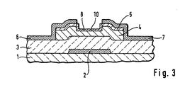
- a thin-film transistor fabricated by a method according an embodiment of the present invention has a gate electrode 2 selectively formed on an insulating substrate 1, a gate insulating film 3 an intrinsic or non-doped amorphous silicon layer 4, an n-type amorphous silicon contact layer 5, a drain electrode 6, and a source electrode 7.
- This transistor further has a p-type amorphous silicon layer 8 on the back channel portion of the amorphous silicon layer 4 between the drain electrode 6 and the source electrode 7 in accordance with the present invention.
- the thickness of p-type amorphous silicon layer 8 is 100 ⁇ or less.
- a protective such as silicon-nitride covers the p-type amorphous silicon layer 8 and a the source and drain electrodes 6 and 7.
- the above thin-film transistor is fabricated as follows:
- the gate electrode 2 made of a metal such as chromium is selectively formed on the insulating substrate 1 made of a glass or the like, followed by forming the gate insulating film 3 made of silicon nitride over the entire surface.
- the intrinsic or non-doped amorphous silicon layer 4 and the n-type amorphous silicon contact layer 5 are thereafter deposited in that order by the plasma CVD method.
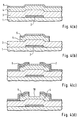
- the amorphous silicon layer 4 and the n-type amorphous silicon contact layer 5 are selectively etched to form an island by the lithography art, as shown in Fig. 4(b).
- a metal film made of chromium or the like is deposited over the entire surface by the sputtering method and then patterned to form the drain electrode 6 and the source electrode 7 as shown in Fig. 4(c).
- the portion of the n-type amorphous silicon contact layer 5 between the drain electrode 6 and the source electrode 7 is removed by using the electrodes as a mask by the wet etching method or the dry etching method in accordance with the present invention. This etching process is carried out until the surface portion of the amorphous silicon layer 4 is removed. That portion of the contact layer 5 is thus completely removed, the surface of the amorphous silicon layer 4 thus exposed serves as a back channel 10, as shown in Fig. 4(d).
- the p-type amorphous silicon layer 8 is then selectively deposited between the drain electrode 6 and the source electrode 7 in accordance also with the present invention. Finally the silicon-nitride protective film 9 is formed.
- the selective deposition of the p-type amorphous silicon layer 8 only on the exposed amorphous silicon layer is performed by mixing disilane Si 2 H 6 , hydrogen H 2 and diborane B 2 H 6 at the ratio of 3:2:6, setting the pressure of the mixed gas to 200 Pa and the substrate temperature to 350°C, and exposing the thin-film transistor shown in Fig. 4(d) to the mixed-gas atmosphere.
- the thickness of the layer 8 is several tens of angstroms though it cannot accurately be measured because the deposition rate is very low. Under the above conditions, the depositing time for the layer 8 can be approx. 15 min. Thereafter, the layer 8 is annealed in the nitrogen atmosphere at 250°C for 30 min.
- silane instead of disilane in the mixed gas.
- silane is not easily decomposed only by raising temperature. Therefore, it is better to use disilane.
- the ratio of disilane Si 2 H 6 to diborane B 2 H 6 of the mixed gas is set to 1:2.
- the ratio of hydrogen gas can be changed within the range of 0 to 10 when assuming the ratio of disilane as 1.
- an inert gas such as argon
- the temperature of the substrate in the range of 300 to 400°C.
- the temperature goes out of the range, it is difficult to perform the vapor-phase epitaxy. Because it is enough to deposit a p-type amorphous silicon layer up to the thickness of 10 to 100 ⁇ in a vapor phase, the layer can be deposited for 10 to 30 min. If the layer is too thick, there is a problem that leak current may flow. If the layer is too thin, it can not be formed uniformly. The annealing time is enough for 30 min to 2 hr.
- the p-type amorphous silicon layer 8 is obtained at a very low deposition rate, it is easily influenced by a substrate due to the same effect as the epitaxial art for single-crystal silicon and thus it is selectively deposited only on the intrinsic amorphous silicon layer 4. Therefore, the layer 8 is preferable because it is hardly deposited on areas of the substrate other than the intrinsic amorphous silicon layer 4. Presence of the p-type amorphous silicon layer 8 can be confirmed by measuring the depth profile through the SIMS element analysis and it is found that boron is present in layers with a thickness of 50 ⁇ or less at a concentration of 10 18 to 10 19 atoms/cm 3 .
- Fig. 5 shows the property of the thin-film transistor of this embodiment.
- the current between drain and source to the gate voltage when applying the voltage of 10 V between the drain and source. From Fig. 5, it is understood that the current between the drain and the source is decreased for the gate voltage of -10 v to 0 V compared to the case of the prior art. That is, the leak current is decreased when the thin-film transistor is off.
- increase of the off current is not recognized even by applying +30 V to the gate electrode and 0 V to the source electrode for 90 min in the air of 80°C. This is because the p-type silicon layer directly contacts the silicon-nitride protective film 9 and a stable interface is formed.
- the p-type amorphous silicon layer 8 with a thickness of several tens of angstroms is formed by mixing silane SiH 4 , hydrogen H 2 , and diborane B 2 H 6 at a mixing ratio of 1:1:2, setting the pressure of the mixed gas to 100 Pa (0.75 Torr), the substrate temperature to 300°C, and the electric power to 25 mW/cm 2 , and discharging electricity for 10 sec.
- the plasma CVD process an advantage is obtained that a p-type amorphous silicon layer can be formed for several tens of seconds though the selectivity is low.
- disilane and diborane for the vapor-phase epitaxy process.
- plasma CVD it is better to use silane and diborane.
- disilane for the plasma CVD.
- disilane is more easily decomposed than silane and therefore it is extremely decomposed due to plasma, disilane is not suitable for the plasma CVD.
- plasma CVD plasma serve as an assistant to decompose silane. Therefore, the combination of disilane and diborane in the vapor-phase epitaxy process corresponds to the combination of silane and diborane in the plasma CVD process.
- the mixing ratio of silane SiH 4 to diborane B 2 H 6 is set to 1:2 and hydrogen H 2 is mixed with the mixture of them in the range of 0 to 5.
- the pressure, substrate temperature, and electric power can be changed in the ranges of 80 to 120 Pa, 250 to 320°C, and 10 to 30 mW/cm 2 respectively. It is necessary to set the discharge time to several seconds to 1 min.
Landscapes
- Thin Film Transistor (AREA)
Applications Claiming Priority (3)
| Application Number | Priority Date | Filing Date | Title |
|---|---|---|---|
| JP8422994 | 1994-04-22 | ||
| JP84229/94 | 1994-04-22 | ||
| JP8422994 | 1994-04-22 |
Publications (3)
| Publication Number | Publication Date |
|---|---|
| EP0678907A2 EP0678907A2 (en) | 1995-10-25 |
| EP0678907A3 EP0678907A3 (en) | 1997-08-20 |
| EP0678907B1 true EP0678907B1 (en) | 2002-02-27 |
Family
ID=13824652
Family Applications (1)
| Application Number | Title | Priority Date | Filing Date |
|---|---|---|---|
| EP95105936A Expired - Lifetime EP0678907B1 (en) | 1994-04-22 | 1995-04-20 | Method for fabricating reverse-staggered thin-film transistor |
Country Status (5)
| Country | Link |
|---|---|
| US (1) | US5561074A (OSRAM) |
| EP (1) | EP0678907B1 (OSRAM) |
| KR (1) | KR0180323B1 (OSRAM) |
| DE (1) | DE69525558T2 (OSRAM) |
| TW (1) | TW291597B (OSRAM) |
Cited By (7)
| Publication number | Priority date | Publication date | Assignee | Title |
|---|---|---|---|---|
| US7652294B2 (en) | 2000-03-08 | 2010-01-26 | Semiconductor Energy Laboratory Co., Ltd. | Semiconductor device and manufacturing method thereof |
| US7656491B2 (en) | 2000-03-16 | 2010-02-02 | Semiconductor Energy Laboratory Co., Ltd. | Liquid crystal display device and method of manufacturing the same |
| US7687325B2 (en) | 2000-03-13 | 2010-03-30 | Semiconductor Energy Laboratory Co., Ltd. | Semiconductor device and manufacturing method thereof |
| US7705354B2 (en) | 2000-03-06 | 2010-04-27 | Semiconductor Energy Laboratory Co., Ltd | Semiconductor device and method for fabricating the same |
| US7714975B1 (en) | 2000-03-17 | 2010-05-11 | Semiconductor Energy Laboratory Co., Ltd | Liquid crystal display device and manfacturing method thereof |
| US7902550B2 (en) | 2000-05-09 | 2011-03-08 | Semiconductor Energy Laboratory Co., Ltd. | Semiconductor device and manufacturing method thereof |
| CN101369587B (zh) * | 2007-08-17 | 2012-05-23 | 株式会社半导体能源研究所 | 显示装置 |
Families Citing this family (9)
| Publication number | Priority date | Publication date | Assignee | Title |
|---|---|---|---|---|
| JP2833545B2 (ja) * | 1995-03-06 | 1998-12-09 | 日本電気株式会社 | 半導体装置の製造方法 |
| JP3082679B2 (ja) * | 1996-08-29 | 2000-08-28 | 日本電気株式会社 | 薄膜トランジスタおよびその製造方法 |
| WO1998057506A1 (en) * | 1997-06-12 | 1998-12-17 | Northern Telecom Limited | Directory service based on geographic location of a mobile telecommunications unit |
| JP2001308339A (ja) | 2000-02-18 | 2001-11-02 | Sharp Corp | 薄膜トランジスタ |
| JP4700160B2 (ja) | 2000-03-13 | 2011-06-15 | 株式会社半導体エネルギー研究所 | 半導体装置 |
| US7071037B2 (en) | 2001-03-06 | 2006-07-04 | Semiconductor Energy Laboratory Co., Ltd. | Semiconductor device and manufacturing method thereof |
| CN100477129C (zh) * | 2006-02-08 | 2009-04-08 | 财团法人工业技术研究院 | 薄膜晶体管、有机电致发光显示元件及其制造方法 |
| WO2009060922A1 (en) * | 2007-11-05 | 2009-05-14 | Semiconductor Energy Laboratory Co., Ltd. | Thin film transistor and display device having the thin film transistor |
| TWI535037B (zh) | 2008-11-07 | 2016-05-21 | 半導體能源研究所股份有限公司 | 半導體裝置和其製造方法 |
Family Cites Families (14)
| Publication number | Priority date | Publication date | Assignee | Title |
|---|---|---|---|---|
| JPS61237420A (ja) * | 1985-04-13 | 1986-10-22 | Oki Electric Ind Co Ltd | P型アモルフアスシリコン薄膜の製造方法 |
| US4882295A (en) * | 1985-07-26 | 1989-11-21 | Energy Conversion Devices, Inc. | Method of making a double injection field effect transistor |
| US5270224A (en) * | 1988-03-11 | 1993-12-14 | Fujitsu Limited | Method of manufacturing a semiconductor device having a region doped to a level exceeding the solubility limit |
| JPH01241175A (ja) * | 1988-03-23 | 1989-09-26 | Seikosha Co Ltd | 非晶質シリコン薄膜トランジスタの製造方法 |
| JPH01302769A (ja) * | 1988-05-30 | 1989-12-06 | Seikosha Co Ltd | 逆スタガー型シリコン薄膜トランジスタの製造方法 |
| US5053354A (en) * | 1988-05-30 | 1991-10-01 | Seikosha Co., Ltd. | Method of fabricating a reverse staggered type silicon thin film transistor |
| JPH07114285B2 (ja) * | 1988-12-16 | 1995-12-06 | 日本電気株式会社 | 薄膜トランジスタの製造方法 |
| US5109260A (en) * | 1989-07-10 | 1992-04-28 | Seikosha Co., Ltd. | Silicon thin film transistor and method for producing the same |
| EP0606114A1 (en) * | 1989-08-11 | 1994-07-13 | Seiko Instruments Inc. | Method of producing field effect transistor |
| JPH04505833A (ja) * | 1990-10-05 | 1992-10-08 | ゼネラル・エレクトリック・カンパニイ | 基準構造の地形の伝搬地形による装置の自己アライメント |
| JPH04321275A (ja) * | 1991-04-19 | 1992-11-11 | Nec Corp | 薄膜トランジスタ |
| JPH04367277A (ja) * | 1991-06-14 | 1992-12-18 | Nec Corp | 薄膜トランジスタおよびその製造方法 |
| JPH04367276A (ja) * | 1991-06-14 | 1992-12-18 | Nec Corp | 薄膜トランジスタおよびその製造方法 |
| JPH0583197A (ja) * | 1991-09-21 | 1993-04-02 | Alpine Electron Inc | デイジタルオーデイオ装置 |
-
1995
- 1995-04-20 US US08/425,806 patent/US5561074A/en not_active Expired - Lifetime
- 1995-04-20 DE DE69525558T patent/DE69525558T2/de not_active Expired - Lifetime
- 1995-04-20 EP EP95105936A patent/EP0678907B1/en not_active Expired - Lifetime
- 1995-04-21 KR KR1019950009475A patent/KR0180323B1/ko not_active Expired - Fee Related
- 1995-04-21 TW TW084103943A patent/TW291597B/zh not_active IP Right Cessation
Cited By (23)
| Publication number | Priority date | Publication date | Assignee | Title |
|---|---|---|---|---|
| US7973312B2 (en) | 2000-03-06 | 2011-07-05 | Semiconductor Energy Laboratory Co., Ltd. | Semiconductor device and method of fabricating the same |
| US9099355B2 (en) | 2000-03-06 | 2015-08-04 | Semiconductor Energy Laboratory Co., Ltd. | Semiconductor device and method of fabricating the same |
| US8188478B2 (en) | 2000-03-06 | 2012-05-29 | Semiconductor Energy Laboratory Co., Ltd. | Semiconductor device and method of fabricating the same |
| US7705354B2 (en) | 2000-03-06 | 2010-04-27 | Semiconductor Energy Laboratory Co., Ltd | Semiconductor device and method for fabricating the same |
| US7728334B2 (en) | 2000-03-08 | 2010-06-01 | Semiconductor Energy Laboratory Co., Ltd. | Semiconductor device and manufacturing method thereof |
| US8586988B2 (en) | 2000-03-08 | 2013-11-19 | Semiconductor Energy Laboratory Co., Ltd. | Semiconductor device and manufacturing method thereof |
| US9786687B2 (en) | 2000-03-08 | 2017-10-10 | Semiconductor Energy Laboratory Co., Ltd. | Semiconductor device and manufacturing method thereof |
| US8198630B2 (en) | 2000-03-08 | 2012-06-12 | Semiconductor Energy Laboratory Co., Ltd. | Semiconductor device and manufacturing method thereof |
| US7652294B2 (en) | 2000-03-08 | 2010-01-26 | Semiconductor Energy Laboratory Co., Ltd. | Semiconductor device and manufacturing method thereof |
| US7687325B2 (en) | 2000-03-13 | 2010-03-30 | Semiconductor Energy Laboratory Co., Ltd. | Semiconductor device and manufacturing method thereof |
| US7656491B2 (en) | 2000-03-16 | 2010-02-02 | Semiconductor Energy Laboratory Co., Ltd. | Liquid crystal display device and method of manufacturing the same |
| US7990508B2 (en) | 2000-03-16 | 2011-08-02 | Semiconductor Energy Laboratory Co., Ltd. | Liquid crystal display device and method of manufacturing the same |
| US8873011B2 (en) | 2000-03-16 | 2014-10-28 | Semiconductor Energy Laboratory Co., Ltd. | Liquid crystal display device and method of manufacturing the same |
| US8228477B2 (en) | 2000-03-16 | 2012-07-24 | Semiconductor Energy Laboratory Co., Ltd. | Liquid crystal display device and method of manufacturing the same |
| US8610861B2 (en) | 2000-03-16 | 2013-12-17 | Semiconductor Energy Laboratory Co., Ltd. | Liquid crystal display device and method of manufacturing the same |
| US8421985B2 (en) | 2000-03-17 | 2013-04-16 | Semiconductor Energy Laboratory Co., Ltd. | Liquid crystal display device and manufacturing method thereof |
| US8558983B2 (en) | 2000-03-17 | 2013-10-15 | Semiconductor Energy Laboratory Co., Ltd. | Liquid crystal display device and manufacturing method thereof |
| US7714975B1 (en) | 2000-03-17 | 2010-05-11 | Semiconductor Energy Laboratory Co., Ltd | Liquid crystal display device and manfacturing method thereof |
| US8525173B2 (en) | 2000-05-09 | 2013-09-03 | Semiconductor Energy Laboratory Co., Ltd. | Semiconductor device and manufacturing method thereof |
| US8823004B2 (en) | 2000-05-09 | 2014-09-02 | Semiconductor Energy Laboratory Co., Ltd. | Semiconductor device and manufacturing method thereof |
| US7902550B2 (en) | 2000-05-09 | 2011-03-08 | Semiconductor Energy Laboratory Co., Ltd. | Semiconductor device and manufacturing method thereof |
| CN101369587B (zh) * | 2007-08-17 | 2012-05-23 | 株式会社半导体能源研究所 | 显示装置 |
| TWI491045B (zh) * | 2007-08-17 | 2015-07-01 | Semiconductor Energy Lab | 顯示裝置 |
Also Published As
| Publication number | Publication date |
|---|---|
| DE69525558T2 (de) | 2002-08-22 |
| EP0678907A2 (en) | 1995-10-25 |
| US5561074A (en) | 1996-10-01 |
| TW291597B (OSRAM) | 1996-11-21 |
| DE69525558D1 (de) | 2002-04-04 |
| KR0180323B1 (ko) | 1999-04-15 |
| EP0678907A3 (en) | 1997-08-20 |
| KR950030282A (ko) | 1995-11-24 |
Similar Documents
| Publication | Publication Date | Title |
|---|---|---|
| EP0678907B1 (en) | Method for fabricating reverse-staggered thin-film transistor | |
| US5189504A (en) | Semiconductor device of MOS structure having p-type gate electrode | |
| US5170231A (en) | Silicon carbide field-effect transistor with improved breakdown voltage and low leakage current | |
| US8110453B2 (en) | Low temperature thin film transistor process, device property, and device stability improvement | |
| US4814842A (en) | Thin film transistor utilizing hydrogenated polycrystalline silicon | |
| EP0036573B1 (en) | Method for making a polysilicon conductor structure | |
| US6703267B2 (en) | Method of manufacturing thin film transistor | |
| US5534445A (en) | Method of fabricating a polysilicon thin film transistor | |
| US6455871B1 (en) | SiGe MODFET with a metal-oxide film and method for fabricating the same | |
| US4741964A (en) | Structure containing hydrogenated amorphous silicon and process | |
| EP0344863B1 (en) | A method of producing a thin film transistor | |
| JP3187086B2 (ja) | 半導体装置および半導体装置の作製方法 | |
| Jin et al. | High-performance polycrystalline SiGe thin-film transistors using Al 2 O 3 gate insulators | |
| JP2000501569A (ja) | 窒化クロムを含む電極を含む電子的デバイス及びこのデバイスの製造方法 | |
| EP0637837A2 (en) | Method for fabricating a thin film transistor | |
| US5216264A (en) | Silicon carbide MOS type field-effect transistor with at least one of the source and drain regions is formed by the use of a schottky contact | |
| KR100272260B1 (ko) | 유사다이아몬드를 이용한 박막트랜지스터 및 그의 제조방법 | |
| US6639279B1 (en) | Semiconductor transistor having interface layer between semiconductor and insulating layers | |
| US5422287A (en) | Thin film transistor and process for producing the same | |
| US5923050A (en) | Amorphous silicon TFT | |
| US6514803B1 (en) | Process for making an amorphous silicon thin film semiconductor device | |
| EP0481777A2 (en) | Method of manufacturing gate insulated field effect transistors | |
| JPH04367277A (ja) | 薄膜トランジスタおよびその製造方法 | |
| Hasegawa et al. | Control of Preferential Orientation in Polycrystalline Silicon Films Prepared by Plasma‐Enhanced Chemical Vapor Deposition | |
| JPH088440A (ja) | 薄膜トランジスタとその製造方法 |
Legal Events
| Date | Code | Title | Description |
|---|---|---|---|
| PUAI | Public reference made under article 153(3) epc to a published international application that has entered the european phase |
Free format text: ORIGINAL CODE: 0009012 |
|
| AK | Designated contracting states |
Kind code of ref document: A2 Designated state(s): DE FR GB |
|
| PUAL | Search report despatched |
Free format text: ORIGINAL CODE: 0009013 |
|
| AK | Designated contracting states |
Kind code of ref document: A3 Designated state(s): DE FR GB |
|
| 17P | Request for examination filed |
Effective date: 19980220 |
|
| 17Q | First examination report despatched |
Effective date: 19980911 |
|
| GRAG | Despatch of communication of intention to grant |
Free format text: ORIGINAL CODE: EPIDOS AGRA |
|
| GRAG | Despatch of communication of intention to grant |
Free format text: ORIGINAL CODE: EPIDOS AGRA |
|
| GRAH | Despatch of communication of intention to grant a patent |
Free format text: ORIGINAL CODE: EPIDOS IGRA |
|
| GRAH | Despatch of communication of intention to grant a patent |
Free format text: ORIGINAL CODE: EPIDOS IGRA |
|
| REG | Reference to a national code |
Ref country code: GB Ref legal event code: IF02 |
|
| GRAA | (expected) grant |
Free format text: ORIGINAL CODE: 0009210 |
|
| AK | Designated contracting states |
Kind code of ref document: B1 Designated state(s): DE FR GB |
|
| REF | Corresponds to: |
Ref document number: 69525558 Country of ref document: DE Date of ref document: 20020404 |
|
| ET | Fr: translation filed | ||
| PLBE | No opposition filed within time limit |
Free format text: ORIGINAL CODE: 0009261 |
|
| STAA | Information on the status of an ep patent application or granted ep patent |
Free format text: STATUS: NO OPPOSITION FILED WITHIN TIME LIMIT |
|
| 26N | No opposition filed |
Effective date: 20021128 |
|
| REG | Reference to a national code |
Ref country code: GB Ref legal event code: 732E |
|
| REG | Reference to a national code |
Ref country code: FR Ref legal event code: TP |
|
| REG | Reference to a national code |
Ref country code: GB Ref legal event code: 732E Free format text: REGISTERED BETWEEN 20100325 AND 20100331 |
|
| REG | Reference to a national code |
Ref country code: GB Ref legal event code: 732E Free format text: REGISTERED BETWEEN 20110728 AND 20110803 |
|
| REG | Reference to a national code |
Ref country code: FR Ref legal event code: TP Owner name: GETNER FOUNDATION LLC, US Effective date: 20110905 |
|
| PGFP | Annual fee paid to national office [announced via postgrant information from national office to epo] |
Ref country code: GB Payment date: 20120327 Year of fee payment: 18 |
|
| REG | Reference to a national code |
Ref country code: DE Ref legal event code: R082 Ref document number: 69525558 Country of ref document: DE Representative=s name: MUELLER-BORE & PARTNER PATENTANWAELTE, EUROPEA, DE |
|
| PGFP | Annual fee paid to national office [announced via postgrant information from national office to epo] |
Ref country code: DE Payment date: 20120430 Year of fee payment: 18 |
|
| PGFP | Annual fee paid to national office [announced via postgrant information from national office to epo] |
Ref country code: FR Payment date: 20120503 Year of fee payment: 18 |
|
| REG | Reference to a national code |
Ref country code: DE Ref legal event code: R082 Ref document number: 69525558 Country of ref document: DE Representative=s name: MUELLER-BORE & PARTNER PATENTANWAELTE PARTG MB, DE Effective date: 20120723 Ref country code: DE Ref legal event code: R081 Ref document number: 69525558 Country of ref document: DE Owner name: GETNER FOUNDATION LLC, US Free format text: FORMER OWNER: NEC CORP., TOKYO, JP Effective date: 20120723 |
|
| GBPC | Gb: european patent ceased through non-payment of renewal fee |
Effective date: 20130420 |
|
| PG25 | Lapsed in a contracting state [announced via postgrant information from national office to epo] |
Ref country code: GB Free format text: LAPSE BECAUSE OF NON-PAYMENT OF DUE FEES Effective date: 20130420 Ref country code: DE Free format text: LAPSE BECAUSE OF NON-PAYMENT OF DUE FEES Effective date: 20131101 |
|
| REG | Reference to a national code |
Ref country code: FR Ref legal event code: ST Effective date: 20131231 |
|
| REG | Reference to a national code |
Ref country code: DE Ref legal event code: R119 Ref document number: 69525558 Country of ref document: DE Effective date: 20131101 |
|
| PG25 | Lapsed in a contracting state [announced via postgrant information from national office to epo] |
Ref country code: FR Free format text: LAPSE BECAUSE OF NON-PAYMENT OF DUE FEES Effective date: 20130430 |