EP0670592A2 - Halbleitervorrichtungen sowie ihre Herstellung unter Verwendung der Kristallorientierungsabhängigheit der Datierungs - Google Patents
Halbleitervorrichtungen sowie ihre Herstellung unter Verwendung der Kristallorientierungsabhängigheit der Datierungs Download PDFInfo
- Publication number
- EP0670592A2 EP0670592A2 EP95301369A EP95301369A EP0670592A2 EP 0670592 A2 EP0670592 A2 EP 0670592A2 EP 95301369 A EP95301369 A EP 95301369A EP 95301369 A EP95301369 A EP 95301369A EP 0670592 A2 EP0670592 A2 EP 0670592A2
- Authority
- EP
- European Patent Office
- Prior art keywords
- plane
- layer
- type
- type region
- group iii
- Prior art date
- Legal status (The legal status is an assumption and is not a legal conclusion. Google has not performed a legal analysis and makes no representation as to the accuracy of the status listed.)
- Granted
Links
Images


Classifications
-
- H—ELECTRICITY
- H01—ELECTRIC ELEMENTS
- H01S—DEVICES USING THE PROCESS OF LIGHT AMPLIFICATION BY STIMULATED EMISSION OF RADIATION [LASER] TO AMPLIFY OR GENERATE LIGHT; DEVICES USING STIMULATED EMISSION OF ELECTROMAGNETIC RADIATION IN WAVE RANGES OTHER THAN OPTICAL
- H01S5/00—Semiconductor lasers
- H01S5/30—Structure or shape of the active region; Materials used for the active region
- H01S5/32—Structure or shape of the active region; Materials used for the active region comprising PN junctions, e.g. hetero- or double- heterostructures
- H01S5/3202—Structure or shape of the active region; Materials used for the active region comprising PN junctions, e.g. hetero- or double- heterostructures grown on specifically orientated substrates, or using orientation dependent growth
-
- B—PERFORMING OPERATIONS; TRANSPORTING
- B82—NANOTECHNOLOGY
- B82Y—SPECIFIC USES OR APPLICATIONS OF NANOSTRUCTURES; MEASUREMENT OR ANALYSIS OF NANOSTRUCTURES; MANUFACTURE OR TREATMENT OF NANOSTRUCTURES
- B82Y20/00—Nanooptics, e.g. quantum optics or photonic crystals
-
- H—ELECTRICITY
- H01—ELECTRIC ELEMENTS
- H01S—DEVICES USING THE PROCESS OF LIGHT AMPLIFICATION BY STIMULATED EMISSION OF RADIATION [LASER] TO AMPLIFY OR GENERATE LIGHT; DEVICES USING STIMULATED EMISSION OF ELECTROMAGNETIC RADIATION IN WAVE RANGES OTHER THAN OPTICAL
- H01S5/00—Semiconductor lasers
- H01S5/10—Construction or shape of the optical resonator, e.g. extended or external cavity, coupled cavities, bent-guide, varying width, thickness or composition of the active region
- H01S5/18—Surface-emitting [SE] lasers, e.g. having both horizontal and vertical cavities
- H01S5/183—Surface-emitting [SE] lasers, e.g. having both horizontal and vertical cavities having only vertical cavities, e.g. vertical cavity surface-emitting lasers [VCSEL]
- H01S5/18344—Surface-emitting [SE] lasers, e.g. having both horizontal and vertical cavities having only vertical cavities, e.g. vertical cavity surface-emitting lasers [VCSEL] characterized by the mesa, e.g. dimensions or shape of the mesa
- H01S5/18352—Mesa with inclined sidewall
-
- H—ELECTRICITY
- H01—ELECTRIC ELEMENTS
- H01S—DEVICES USING THE PROCESS OF LIGHT AMPLIFICATION BY STIMULATED EMISSION OF RADIATION [LASER] TO AMPLIFY OR GENERATE LIGHT; DEVICES USING STIMULATED EMISSION OF ELECTROMAGNETIC RADIATION IN WAVE RANGES OTHER THAN OPTICAL
- H01S5/00—Semiconductor lasers
- H01S5/20—Structure or shape of the semiconductor body to guide the optical wave ; Confining structures perpendicular to the optical axis, e.g. index or gain guiding, stripe geometry, broad area lasers, gain tailoring, transverse or lateral reflectors, special cladding structures, MQW barrier reflection layers
- H01S5/22—Structure or shape of the semiconductor body to guide the optical wave ; Confining structures perpendicular to the optical axis, e.g. index or gain guiding, stripe geometry, broad area lasers, gain tailoring, transverse or lateral reflectors, special cladding structures, MQW barrier reflection layers having a ridge or stripe structure
- H01S5/223—Buried stripe structure
- H01S5/2238—Buried stripe structure with a terraced structure
-
- H—ELECTRICITY
- H01—ELECTRIC ELEMENTS
- H01S—DEVICES USING THE PROCESS OF LIGHT AMPLIFICATION BY STIMULATED EMISSION OF RADIATION [LASER] TO AMPLIFY OR GENERATE LIGHT; DEVICES USING STIMULATED EMISSION OF ELECTROMAGNETIC RADIATION IN WAVE RANGES OTHER THAN OPTICAL
- H01S5/00—Semiconductor lasers
- H01S5/30—Structure or shape of the active region; Materials used for the active region
- H01S5/305—Structure or shape of the active region; Materials used for the active region characterised by the doping materials used in the laser structure
-
- H—ELECTRICITY
- H10—SEMICONDUCTOR DEVICES; ELECTRIC SOLID-STATE DEVICES NOT OTHERWISE PROVIDED FOR
- H10D—INORGANIC ELECTRIC SEMICONDUCTOR DEVICES
- H10D10/00—Bipolar junction transistors [BJT]
- H10D10/01—Manufacture or treatment
- H10D10/021—Manufacture or treatment of heterojunction BJTs [HBT]
-
- H—ELECTRICITY
- H10—SEMICONDUCTOR DEVICES; ELECTRIC SOLID-STATE DEVICES NOT OTHERWISE PROVIDED FOR
- H10D—INORGANIC ELECTRIC SEMICONDUCTOR DEVICES
- H10D30/00—Field-effect transistors [FET]
- H10D30/01—Manufacture or treatment
- H10D30/015—Manufacture or treatment of FETs having heterojunction interface channels or heterojunction gate electrodes, e.g. HEMT
-
- H—ELECTRICITY
- H10—SEMICONDUCTOR DEVICES; ELECTRIC SOLID-STATE DEVICES NOT OTHERWISE PROVIDED FOR
- H10D—INORGANIC ELECTRIC SEMICONDUCTOR DEVICES
- H10D62/00—Semiconductor bodies, or regions thereof, of devices having potential barriers
- H10D62/40—Crystalline structures
- H10D62/405—Orientations of crystalline planes
-
- H—ELECTRICITY
- H10—SEMICONDUCTOR DEVICES; ELECTRIC SOLID-STATE DEVICES NOT OTHERWISE PROVIDED FOR
- H10P—GENERIC PROCESSES OR APPARATUS FOR THE MANUFACTURE OR TREATMENT OF DEVICES COVERED BY CLASS H10
- H10P14/00—Formation of materials, e.g. in the shape of layers or pillars
- H10P14/20—Formation of materials, e.g. in the shape of layers or pillars of semiconductor materials
- H10P14/24—Formation of materials, e.g. in the shape of layers or pillars of semiconductor materials using chemical vapour deposition [CVD]
-
- H—ELECTRICITY
- H10—SEMICONDUCTOR DEVICES; ELECTRIC SOLID-STATE DEVICES NOT OTHERWISE PROVIDED FOR
- H10P—GENERIC PROCESSES OR APPARATUS FOR THE MANUFACTURE OR TREATMENT OF DEVICES COVERED BY CLASS H10
- H10P14/00—Formation of materials, e.g. in the shape of layers or pillars
- H10P14/20—Formation of materials, e.g. in the shape of layers or pillars of semiconductor materials
- H10P14/27—Formation of materials, e.g. in the shape of layers or pillars of semiconductor materials using selective deposition, e.g. simultaneous growth of monocrystalline and non-monocrystalline semiconductor materials
-
- H—ELECTRICITY
- H10—SEMICONDUCTOR DEVICES; ELECTRIC SOLID-STATE DEVICES NOT OTHERWISE PROVIDED FOR
- H10P—GENERIC PROCESSES OR APPARATUS FOR THE MANUFACTURE OR TREATMENT OF DEVICES COVERED BY CLASS H10
- H10P14/00—Formation of materials, e.g. in the shape of layers or pillars
- H10P14/20—Formation of materials, e.g. in the shape of layers or pillars of semiconductor materials
- H10P14/29—Formation of materials, e.g. in the shape of layers or pillars of semiconductor materials characterised by the substrates
- H10P14/2901—Materials
- H10P14/2907—Materials being Group IIIA-VA materials
- H10P14/2911—Arsenides
-
- H—ELECTRICITY
- H10—SEMICONDUCTOR DEVICES; ELECTRIC SOLID-STATE DEVICES NOT OTHERWISE PROVIDED FOR
- H10P—GENERIC PROCESSES OR APPARATUS FOR THE MANUFACTURE OR TREATMENT OF DEVICES COVERED BY CLASS H10
- H10P14/00—Formation of materials, e.g. in the shape of layers or pillars
- H10P14/20—Formation of materials, e.g. in the shape of layers or pillars of semiconductor materials
- H10P14/29—Formation of materials, e.g. in the shape of layers or pillars of semiconductor materials characterised by the substrates
- H10P14/2924—Structures
- H10P14/2925—Surface structures
-
- H—ELECTRICITY
- H10—SEMICONDUCTOR DEVICES; ELECTRIC SOLID-STATE DEVICES NOT OTHERWISE PROVIDED FOR
- H10P—GENERIC PROCESSES OR APPARATUS FOR THE MANUFACTURE OR TREATMENT OF DEVICES COVERED BY CLASS H10
- H10P14/00—Formation of materials, e.g. in the shape of layers or pillars
- H10P14/20—Formation of materials, e.g. in the shape of layers or pillars of semiconductor materials
- H10P14/29—Formation of materials, e.g. in the shape of layers or pillars of semiconductor materials characterised by the substrates
- H10P14/2926—Crystal orientations
-
- H—ELECTRICITY
- H10—SEMICONDUCTOR DEVICES; ELECTRIC SOLID-STATE DEVICES NOT OTHERWISE PROVIDED FOR
- H10P—GENERIC PROCESSES OR APPARATUS FOR THE MANUFACTURE OR TREATMENT OF DEVICES COVERED BY CLASS H10
- H10P14/00—Formation of materials, e.g. in the shape of layers or pillars
- H10P14/20—Formation of materials, e.g. in the shape of layers or pillars of semiconductor materials
- H10P14/32—Formation of materials, e.g. in the shape of layers or pillars of semiconductor materials characterised by intermediate layers between substrates and deposited layers
- H10P14/3202—Materials thereof
- H10P14/3214—Materials thereof being Group IIIA-VA semiconductors
- H10P14/3221—Arsenides
-
- H—ELECTRICITY
- H10—SEMICONDUCTOR DEVICES; ELECTRIC SOLID-STATE DEVICES NOT OTHERWISE PROVIDED FOR
- H10P—GENERIC PROCESSES OR APPARATUS FOR THE MANUFACTURE OR TREATMENT OF DEVICES COVERED BY CLASS H10
- H10P14/00—Formation of materials, e.g. in the shape of layers or pillars
- H10P14/20—Formation of materials, e.g. in the shape of layers or pillars of semiconductor materials
- H10P14/32—Formation of materials, e.g. in the shape of layers or pillars of semiconductor materials characterised by intermediate layers between substrates and deposited layers
- H10P14/3242—Structure
- H10P14/3244—Layer structure
- H10P14/3251—Layer structure consisting of three or more layers
-
- H—ELECTRICITY
- H10—SEMICONDUCTOR DEVICES; ELECTRIC SOLID-STATE DEVICES NOT OTHERWISE PROVIDED FOR
- H10P—GENERIC PROCESSES OR APPARATUS FOR THE MANUFACTURE OR TREATMENT OF DEVICES COVERED BY CLASS H10
- H10P14/00—Formation of materials, e.g. in the shape of layers or pillars
- H10P14/20—Formation of materials, e.g. in the shape of layers or pillars of semiconductor materials
- H10P14/32—Formation of materials, e.g. in the shape of layers or pillars of semiconductor materials characterised by intermediate layers between substrates and deposited layers
- H10P14/3258—Crystal orientation
-
- H—ELECTRICITY
- H10—SEMICONDUCTOR DEVICES; ELECTRIC SOLID-STATE DEVICES NOT OTHERWISE PROVIDED FOR
- H10P—GENERIC PROCESSES OR APPARATUS FOR THE MANUFACTURE OR TREATMENT OF DEVICES COVERED BY CLASS H10
- H10P14/00—Formation of materials, e.g. in the shape of layers or pillars
- H10P14/20—Formation of materials, e.g. in the shape of layers or pillars of semiconductor materials
- H10P14/34—Deposited materials, e.g. layers
- H10P14/3402—Deposited materials, e.g. layers characterised by the chemical composition
- H10P14/3414—Deposited materials, e.g. layers characterised by the chemical composition being group IIIA-VIA materials
- H10P14/3421—Arsenides
-
- H—ELECTRICITY
- H10—SEMICONDUCTOR DEVICES; ELECTRIC SOLID-STATE DEVICES NOT OTHERWISE PROVIDED FOR
- H10P—GENERIC PROCESSES OR APPARATUS FOR THE MANUFACTURE OR TREATMENT OF DEVICES COVERED BY CLASS H10
- H10P14/00—Formation of materials, e.g. in the shape of layers or pillars
- H10P14/20—Formation of materials, e.g. in the shape of layers or pillars of semiconductor materials
- H10P14/34—Deposited materials, e.g. layers
- H10P14/3438—Doping during depositing
- H10P14/3441—Conductivity type
- H10P14/3442—N-type
-
- H—ELECTRICITY
- H10—SEMICONDUCTOR DEVICES; ELECTRIC SOLID-STATE DEVICES NOT OTHERWISE PROVIDED FOR
- H10P—GENERIC PROCESSES OR APPARATUS FOR THE MANUFACTURE OR TREATMENT OF DEVICES COVERED BY CLASS H10
- H10P14/00—Formation of materials, e.g. in the shape of layers or pillars
- H10P14/20—Formation of materials, e.g. in the shape of layers or pillars of semiconductor materials
- H10P14/34—Deposited materials, e.g. layers
- H10P14/3438—Doping during depositing
- H10P14/3441—Conductivity type
- H10P14/3444—P-type
-
- H—ELECTRICITY
- H01—ELECTRIC ELEMENTS
- H01S—DEVICES USING THE PROCESS OF LIGHT AMPLIFICATION BY STIMULATED EMISSION OF RADIATION [LASER] TO AMPLIFY OR GENERATE LIGHT; DEVICES USING STIMULATED EMISSION OF ELECTROMAGNETIC RADIATION IN WAVE RANGES OTHER THAN OPTICAL
- H01S2304/00—Special growth methods for semiconductor lasers
- H01S2304/04—MOCVD or MOVPE
-
- H—ELECTRICITY
- H01—ELECTRIC ELEMENTS
- H01S—DEVICES USING THE PROCESS OF LIGHT AMPLIFICATION BY STIMULATED EMISSION OF RADIATION [LASER] TO AMPLIFY OR GENERATE LIGHT; DEVICES USING STIMULATED EMISSION OF ELECTROMAGNETIC RADIATION IN WAVE RANGES OTHER THAN OPTICAL
- H01S5/00—Semiconductor lasers
- H01S5/20—Structure or shape of the semiconductor body to guide the optical wave ; Confining structures perpendicular to the optical axis, e.g. index or gain guiding, stripe geometry, broad area lasers, gain tailoring, transverse or lateral reflectors, special cladding structures, MQW barrier reflection layers
- H01S5/22—Structure or shape of the semiconductor body to guide the optical wave ; Confining structures perpendicular to the optical axis, e.g. index or gain guiding, stripe geometry, broad area lasers, gain tailoring, transverse or lateral reflectors, special cladding structures, MQW barrier reflection layers having a ridge or stripe structure
- H01S5/223—Buried stripe structure
- H01S5/2232—Buried stripe structure with inner confining structure between the active layer and the lower electrode
- H01S5/2234—Buried stripe structure with inner confining structure between the active layer and the lower electrode having a structured substrate surface
- H01S5/2235—Buried stripe structure with inner confining structure between the active layer and the lower electrode having a structured substrate surface with a protrusion
-
- H—ELECTRICITY
- H01—ELECTRIC ELEMENTS
- H01S—DEVICES USING THE PROCESS OF LIGHT AMPLIFICATION BY STIMULATED EMISSION OF RADIATION [LASER] TO AMPLIFY OR GENERATE LIGHT; DEVICES USING STIMULATED EMISSION OF ELECTROMAGNETIC RADIATION IN WAVE RANGES OTHER THAN OPTICAL
- H01S5/00—Semiconductor lasers
- H01S5/20—Structure or shape of the semiconductor body to guide the optical wave ; Confining structures perpendicular to the optical axis, e.g. index or gain guiding, stripe geometry, broad area lasers, gain tailoring, transverse or lateral reflectors, special cladding structures, MQW barrier reflection layers
- H01S5/22—Structure or shape of the semiconductor body to guide the optical wave ; Confining structures perpendicular to the optical axis, e.g. index or gain guiding, stripe geometry, broad area lasers, gain tailoring, transverse or lateral reflectors, special cladding structures, MQW barrier reflection layers having a ridge or stripe structure
- H01S5/223—Buried stripe structure
- H01S5/2237—Buried stripe structure with a non-planar active layer
-
- H—ELECTRICITY
- H01—ELECTRIC ELEMENTS
- H01S—DEVICES USING THE PROCESS OF LIGHT AMPLIFICATION BY STIMULATED EMISSION OF RADIATION [LASER] TO AMPLIFY OR GENERATE LIGHT; DEVICES USING STIMULATED EMISSION OF ELECTROMAGNETIC RADIATION IN WAVE RANGES OTHER THAN OPTICAL
- H01S5/00—Semiconductor lasers
- H01S5/30—Structure or shape of the active region; Materials used for the active region
- H01S5/305—Structure or shape of the active region; Materials used for the active region characterised by the doping materials used in the laser structure
- H01S5/3077—Structure or shape of the active region; Materials used for the active region characterised by the doping materials used in the laser structure plane dependent doping
- H01S5/3081—Structure or shape of the active region; Materials used for the active region characterised by the doping materials used in the laser structure plane dependent doping using amphoteric doping
-
- H—ELECTRICITY
- H01—ELECTRIC ELEMENTS
- H01S—DEVICES USING THE PROCESS OF LIGHT AMPLIFICATION BY STIMULATED EMISSION OF RADIATION [LASER] TO AMPLIFY OR GENERATE LIGHT; DEVICES USING STIMULATED EMISSION OF ELECTROMAGNETIC RADIATION IN WAVE RANGES OTHER THAN OPTICAL
- H01S5/00—Semiconductor lasers
- H01S5/30—Structure or shape of the active region; Materials used for the active region
- H01S5/34—Structure or shape of the active region; Materials used for the active region comprising quantum well or superlattice structures, e.g. single quantum well [SQW] lasers, multiple quantum well [MQW] lasers or graded index separate confinement heterostructure [GRINSCH] lasers
- H01S5/343—Structure or shape of the active region; Materials used for the active region comprising quantum well or superlattice structures, e.g. single quantum well [SQW] lasers, multiple quantum well [MQW] lasers or graded index separate confinement heterostructure [GRINSCH] lasers in AIIIBV compounds, e.g. AlGaAs-laser, InP-based laser
- H01S5/34326—Structure or shape of the active region; Materials used for the active region comprising quantum well or superlattice structures, e.g. single quantum well [SQW] lasers, multiple quantum well [MQW] lasers or graded index separate confinement heterostructure [GRINSCH] lasers in AIIIBV compounds, e.g. AlGaAs-laser, InP-based laser with a well layer based on InGa(Al)P, e.g. red laser
-
- H—ELECTRICITY
- H10—SEMICONDUCTOR DEVICES; ELECTRIC SOLID-STATE DEVICES NOT OTHERWISE PROVIDED FOR
- H10D—INORGANIC ELECTRIC SEMICONDUCTOR DEVICES
- H10D62/00—Semiconductor bodies, or regions thereof, of devices having potential barriers
- H10D62/80—Semiconductor bodies, or regions thereof, of devices having potential barriers characterised by the materials
- H10D62/85—Semiconductor bodies, or regions thereof, of devices having potential barriers characterised by the materials being Group III-V materials, e.g. GaAs
Definitions
- the present invention relates to a manufacture of a semiconductor device, and more particularly to a technology of manufacturing a semiconductor device with a p-n junction or junctions formed by using group III-V compound semiconductor.
- a conventional compound semiconductor device has been formed mainly on a flat substrate, particularly a substrate having a flat surface of crystallographic (1 0 0) plane, and made of GaAs, InP or other compound semiconductors, because a semiconductor crystal of excellent quality can be epitaxially grown relatively easily on the substrate having the (1 0 0) plane and also because a flat wafer can be easily cleaved to fine or minute semiconductor devices.
- semiconductor devices having a new structure has been studied recently by epitaxially growing a semiconductor crystal on a semiconductor substrate having not only a flat (1 0 0) plane surface but also other surfaces of other crystal orientations as well as steps, grooves, or ridges. It is expected that semiconductor devices having an excellent performance difficult to be realized on a (1 0 0) plane substrate can be manufactured by using substrates having surfaces of crystal orientations other than the (1 0 0) plane as well as steps, grooves, or ridges.
- the inventors have studied the crystal orientation dependence of the doping characteristics of dopants in group III-V compound semiconductors grown by metal organic vapor phase epitaxy (MOVPE), by using dopants such as group II acceptors (Zn and Mg), group VI donors (Se), and group IV donors (Si).
- MOVPE metal organic vapor phase epitaxy
- dopants such as group II acceptors (Zn and Mg), group VI donors (Se), and group IV donors (Si).
- group II acceptors Zn and Mg
- group VI donors Se
- Si group IV donors
- a method of manufacturing a semiconductor device including the steps of preparing a substrate made of group III-V compound semiconductor and having a flat surface exposing a (n 1 1)A plane (n is a real number of about 1 ⁇ n ⁇ about 3), epitaxially growing an n-type collector layer on the substrate, epitaxially growing a p-type base layer containing carbon as a p-type impurity on the collector layer, and epitaxially growing an n-type emitter layer on the base layer, the emitter layer being made of a material having a forbidden band width wider than that of the base layer.
- a method of manufacturing a semiconductor device including the steps of preparing a substrate made of group III-V compound semiconductor and having a surface crystal orientation tilted by an angle in a range larger than 0° and equal to or smaller than 35° from a (1 0 0) plane to a (1 1 1)B plane or a surface crystal orientation tilted by an angle in a range larger than 0° and smaller than 25° from the (1 0 0) plane to a (1 1 1)A plane, epitaxially growing an electron transfer layer on the substrate without intentionally doping impurities, by using organic metal containing carbon as a group III source material or as a group V source material, and epitaxially growing an electron supply layer made of a material having a forbidden band width wider than that of the electron transfer layer.
- a method of manufacturing a semiconductor device including the steps of preparing a stepped substrate made of group III-V compound semiconductor and having a flat surface exposing a (1 0 0) plane and a slanted surface exposing an (n 1 1)B plane (n is a real number of about 1 ⁇ n) or an (m 1 1)A plane (m is a real number of about 4 ⁇ m), and epitaxially growing group III-V compound semiconductor on the stepped substrate by doping carbon as an impurity under the conditions that the grown epitaxial layer has an n-type region on the slanted surface and a p-type region on the flat surface.
- a method of manufacturing a semiconductor device including the steps of preparing a stepped substrate made of group III-V compound semiconductor and having a flat surface exposing a (1 0 0) plane and a slanted surface exposing a (n 1 1)B plane (n is a real number of about 1 ⁇ n), and epitaxially growing group III-V compound semiconductor on the stepped substrate by doping carbon as an impurity and an n-type impurity at the same time or alternately under the conditions that the grown epitaxial layer has an n-type region on the slanted surface and a p-type region on the flat surface.
- the plane defined by using “about i” includes the plane defined by "i” and other planes tilted therefrom by +/- 5°.
- An epitaxial layer formed on a substrate exposing an (n 1 1)A plane incorporates more carbon as p-type impurities than on (1 0 0) plane. Therefore, by using a substrate exposing such a plane, an epitaxial layer having a high hole concentration can be formed easily.
- a base layer of an HBT (hetero bipolar transistor) having a high hole concentration can be formed easily, so that the performance of HBT can be improved.
- An epitaxial layer formed on a substrate exposing a crystal orientation plane tilted by an angle in the range larger than 0° and equal to or smaller than 35° from a (1 0 0) plane to a (1 1 1)B plane has a small incorporation probability of carbon than (1 0 0) plane.
- a p-type or n-type epitaxial layer can be selectively formed depending upon the crystal orientation of the growth surface, by using a group III source material containing carbon and selecting a proper V/III ratio.
- a p-type region and an n-type region can be selectively formed and patterned in an epitaxial layer by using a substrate having a surface exposing a p-type forming plane and a surface exposing an n-type forming plane.
- a p-type region and an n-type region can also be formed and patterned in an epitaxial layer depending upon the crystal orientation of the growth surface, even if carbon and Si are doped at the same time.
- carbon can be doped in an epitaxial layer of group III-V compound semiconductor to a higher concentration than using a (1 0 0) plane, or conversely the incorporation or capture amount of carbon can be suppressed more than using the (1 0 0) plane. Therefore, high performance semiconductor devices such as HBT and HEMT can be manufactured.
- Fig.1 is a graph showing a crystal orientation dependence of a carbon concentration and a carrier concentration in GaAs epitaxial layers formed by MOVPE.
- Fig.2 is a graph showing a crystal orientation dependence of a carbon concentration and a carrier concentration in AlGaAs epitaxial layers formed by MOVPE.
- Figs.3A and 3B are cross sectional views of a HBT and an HEMT according to first and second embodiments of the invention.
- Fig.4 is a graph showing a V/III ratio dependence of a carrier concentration in GaAs epitaxial layers formed by MOVPE.
- Figs.5A to 5C are cross sectional views of substrates illustrating the selective formation of n-type and p-type regions by positively using a different V/III ratio dependence of a carrier concentration on crystal orientation.
- Fig.6 is a graph showing a crystal orientation dependence of a Si concentration and a carrier concentration in GaAs epitaxial layers formed by MOVPE.
- Fig.7 is a graph showing a crystal orientation dependence of a carbon concentration, a Si concentration, and a carrier concentration in GaAs epitaxial layers formed by MOVPE.
- Figs.8A to 8C are cross sectional views of substrates illustrating the selective formation of n-type and p-type regions by positively using different crystal orientation dependence between a carbon concentration and a Si concentration.
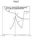
- Fig.9 is a graph showing a crystal orientation dependence of a carbon concentration, a Se concentration, and a carrier concentration in GaAs epitaxial layers formed by MOVPE.
- Figs.10A and 10B are cross sectional views of substrates illustrating the selective formation of n-type and p-type regions by positively using different crystal orientation dependence between a carbon concentration and an Se concentration.
- Fig.11 is a cross sectional view of a semiconductor laser according to a third embodiment of the invention.
- Fig. 12 is a cross sectional view of a semiconductor laser according to a fourth embodiment of the invention.
- Fig.13 is a cross sectional view of a semiconductor laser according to a fifth embodiment of the invention.
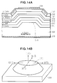
- Figs.14A and 14B are a cross sectional view and a perspective view of a semiconductor laser according to a sixth embodiment of the invention.
- Fig.1 is a graph showing a crystal orientation dependence of a carbon concentration and a hole concentration of carbon-doped GaAs epitaxial layers grown by MOVPE.
- the abscissa represents an offset angle of the plane of a GaAs substrate from a (1 0 0) plane.
- the center of the abscissa is a (1 0 0) plane, the right side from the center shows an offset angle of the substrate tilted in the [0 1 1] direction, and the left side from the center shows an offset angle of the substrate tilted in the [0 1 1 ⁇ ] direction. That is to say, the right side half of Fig.1 shows A planes, and the left side half shows B planes. Typical low Miller indices planes are also shown at respective corresponding offset angles in Fig.1.
- the ordinate represents a carbon or a hole concentration in the unit of cm ⁇ 3.
- Epitaxial layers were grown under a pressure of 6.6 x 10³ Pa and an AsH3 partial pressure of 5.5 Pa by using trimethyl gallium (TMGa) as the group III source material and arsine (AsH3) as the group V shape material.
- TMGa trimethyl gallium
- AsH3 arsine
- Fig.1 an open circle symbol represents a carbon concentration and a solid circle symbol represents a hole concentration, respectively, in each epitaxial layer grown at a substrate temperature of 720°C.
- An open triangle symbol represents a hole concentration in each epitaxial layer grown at a substrate temperature of 690°C.
- the carbon concentration was measured by secondary ion mass spectrometry, and the hole concentration was measured from the C-V characteristic curve. Since both the measured values are generally equal, it can be understood that carbon atoms captured in the crystal are almost perfectly ionized (activated).
- the hole concentration gradually lowers as the offset angle increases.
- the offset angle is further increased toward about 25°, the (3 1 1)A plane, the hole concentration increases abruptly, about ten times as high as that at the (1 0 0) plane.
- the hole concentration scarcely changes as the offset angle is further increased from the (3 1 1)A plane.
- the hole concentration gradually lowers as the offset angle increases, similar to the A plane.
- the hole concentration takes a minimum value between the (3 1 1) B plane and the (2 1 1)B plane. AS the offset angle is further increased, the hole concentration changes to have a higher value.
- the crystal orientation dependence of a hole concentration has a similar tendency both at the substrate temperatures of 720° and 690°.
- the hole concentration and the carbon concentration are generally equal.
- the crystal orientation dependence of the hole concentration is therefore considered to reflect that of the carbon concentration.
- the concentration of captured carbon atoms greatly depends upon the crystal orientation. The above experiments first revealed such complicated dependence.
- Epitaxial layers were grown under a pressure of 6.6 x 10³ Pa and a substrate temperature of 720°C by using trimethyl aluminum (TMAl), and TMCa or triethyl gallium (TEGa) as the group III source material and arsine (AsH3) as the group V source material.
- TMAl trimethyl aluminum
- TMCa triethyl gallium
- AsH3 arsine
- an open circle symbol represents a carbon concentration.
- a solid circle symbol, an open square symbol, and an open triangle symbol represent a hole concentration.
- Use of TEGa as the Ga source material pertains to the open circle symbol, solid circle symbol, and open square symbol
- use of TMGa as the Ga source material pertains to the open triangle symbol.
- An AsH3 partial pressure of 5.5 Pa pertains to the open circle symbol and solid circle symbol, and that of 43 Pa pertains to the open square symbol and open triangle symbol.
- the hole concentration gradually lowers as the offset angle increases. As the offset angle is further increased, the hole concentration changes to have a higher value.
- a change in the hole concentration with the offset angle from the (100) plane of the substrate has a similar tendency both for TEGa and TMGa used as the Ga source material.
- a change in the hole concentration with the offset angle has a similar tendency both for the AsH3 partial pressures of 5.5 Pa and 43 Pa, although the former pressure indicates a higher hole concentration than the latter pressure.
- Such a crystal orientation dependence of a hole concentration can be used in manufacturing various types of semiconductor devices. For example, it can be seen that if p-type impurities are desired to be doped at a high concentration, it is preferable to use the plane in the range from the (3 1 1)A plane to the (1 1 1)A plane rather than to use the (1 0 0) plane. Conversely, if contamination by carbon impurities is desired to be suppressed as much as possible, it can be seen that it is more preferable to use the plane in the range from the (4 1 1)A plane to the plane near the (5 1 1)A plane or the plane in the range from the (3 1 1) B plane to the plane near the (2 1 1)B plane, than the (1 0 0) plane.
- Fig.3A is a cross sectional view of the hetero bipolar transistor (HBT) according to the first embodiment of the invention.
- HBT hetero bipolar transistor
- Each layer was grown by MOVPE under the conditions of a growth temperature of 670 to 730° and a growth pressure of 6 x 10³ to 1.0 x 10⁴ Pa.
- TMAl was used as the Al source material
- TMGa or TEGa was used as the Ga source material
- AsH3 was used as the As source material
- hydrogen was used as a carrier gas
- a total gas flow was set to 8 l/min.
- the electron concentration of the n+-type GaAs substrate 1 was 4 x 1018cm ⁇ 3.
- the electron concentration of the n+-type GaAs buffer layer 2 was 4 x 1018cm ⁇ 3 and the film thickness thereof was 1.0 ⁇ m.
- the electron concentration of the n-type GaAs collector layer 3 was 4 x 1018cm ⁇ 3 and the film thickness thereof was 0.5 ⁇ m.
- the hole concentration of the p+-type GaAs base layer 4 was 1018 to 1020 cm ⁇ 3 and the film thickness thereof was 0.01 to 0.1 ⁇ m.
- the electron concentration of the n-type Al x Ga 1-x As emitter layer 5 was 1 x 1018cm ⁇ 3 and the film thickness thereof was 0.5 ⁇ m.
- the electron concentration of the n+-type GaAs cap layer 6 was 4 x 1018cm ⁇ 3 and the film thickness thereof was 0.1 ⁇ m.
- n'-type GaAs cap layer 6 and n-type AlGaAs emitter layer 5 are being selectively etched to leave a necessary emitter region and expose a partial surface of the p+-type GaAs base layer 4.
- a base electrode 8 of AuZn is being formed on the exposed surface of the p+-type GaAs base layer 4, and an emitter electrode 9 of AuGe is being formed on the surface of the unetched n+-type GaAs cap layer 6.
- the n-type GaAs collector layer 3 is being etched to the region near the outside edge of the base electrode 8, to form a second mesa structure.
- a collector electrode 7 of AuGe is formed on the lower surface of the n+-type GaAs substrate.
- An HBT is required to dope impurities in a very thin base region to a high concentration. It is therefore necessary to change a dope amount very sharply.
- the (3 1 1)A plane substrate carbon atoms can be doped about ten times more than using a (1 0 0) substrate, as explained with Fig.1. It is therefore possible to form a very thin, high impurity concentration base region with ease.
- a similar high carbon concentration can be achieved by using the (2 1 1)A plane or the (1 1 1)A plane in place of the (3 1 1)A plane.
- Fig.3B is a cross sectional view of a high electron mobility transistor according to the second embodiment of the invention.
- GaAs buffer layer 11 an undoped GaAs electron transfer layer 12
- spacer layer 13 a Si- or Se-doped n-type Al x Ga 1-x As (e.g.
- x 0.3
- the n+-type GaAs contact layer 15 is selectively etched to form an opening whose bottom exposes the surface of the electron supply layer 14.
- a Schottky contact gate electrode 18 of Al is formed on the exposed surface of the electron supply layer 14.
- a source electrode 16 and a drain electrode 17, both of AuGe, respectively in contact with the n+-type GaAs contact layer 15 are formed on the surface of the contact layer 15 left on both sides of the opening.
- a HEMT is required to have an electron transfer layer of high purity, i.e. with less residual impurities, in order to make an electron mobility as high as possible and to suppress the side gate effects in an integrated device.
- Main residual impurities in an GaAs layer formed by MOVPE are C or Si.
- a substrate having a crystal orientation tilted from the (1 0 0) plane toward the (1 1 1)B plane allows to suppress the dope amount of C more than using the (1 0 0) plane.
- the offset angle from the (1 0 0) plane is about 35° or larger, the surface conditions of the substrate become bad. It is therefore preferable to set the offset angle to 35° or smaller.
- the plane such as a (4 1 1)A plane, tilted by an angle in the range larger than 0° and smaller than 25°, from the (1 0 0) plane to the (1 1 1)A plane, may also be used which has a small carbon capture amount.
- Material containing As such as InGaAs may be used for the electron transfer layer, with similar advantageous effects being ensured by a proper selection of crystal orientation.
- Fig.4 is a graph showing a change in a carrier concentration in a C-doped GaAs layer formed by MOVPE relative to a V/III ratio or an AsH3 partial pressure.
- the abscissa represents a V/III ratio or AsH3 partial pressure in an arbitrary scale.
- the ordinate represents a carrier concentration in an arbitrary scale.
- Curves a1, b1, and c1 represent hole concentrations in C-doped GaAs layers formed on substrates respectively having a (3 1 1)B plane or a (4 1 1)A plane, a (1 0 0) plane, and a (3 1 1)A plane.
- Curves a2, b2, and c2 represent electron concentrations.
- the capture of carbon elements is suppressed and the hole concentration reduces irrespective of the crystal orientation of a substrate.
- the conductivity type is inverted from the p-type to the n-type and the electron concentration increases.
- the V/III ratio at which the p-type is inverted to the n-type changes with the crystal orientation of a substrate.
- the V/III ratio at which the p-type is inverted to the n-type becomes large in the order of the (3 1 1)B plane or (4 1 1)A plane, the (1 0 0) plane, and the (3 1 1)A plane.
- a ridge 24 is being formed which has a flat surface of the (1 0 0) plane and slanted surfaces of a (3 1 1)B plane, a (4 1 1)A plane, or another plane having a carbon capture amount smaller than the (1 0 0) plane.
- the ridge 24 may be formed by wet etching using a resist mask.
- the slanted surface formed by wet etching is not a surface having a single crystal orientation but contains other surfaces near the (3 1 1)B plane or (4 1 1)A plane. These surfaces are considered to have similar function as the (3 1 1)B plane or (4 1 1)A plane.
- the flat surface and slanted surfaces are each described to have a single crystal orientation, it is intended that they may have other crystal orientations conceivable to have similar functions.
- an epitaxial layer 21 is formed on the whole surface of a substrate 20.
- an epitaxial layer 22 is formed which has a p-type region on the flat surface of the (1 0 0) plane and an n-type region on the slanted surface of the (3 1 1)B plane or (4 1 1)A plane. Therefore, an epitaxial layer having a stripe-shaped n-type region 22b between p-type regions 22a can be formed by the single film forming process.
- an n-type epitaxial layer 23 is formed on the whole surface of the substrate.
- the p-type epitaxial layer 21 grown under the condition of the V/III ratio of K1 has different hole concentrations at the region under the flat surface and the regions under the slanted surface, the hole concentration under the flat surface being higher than that under the slanted surface.
- the slanted surface having the (3 1 1)B plane or (4 1 1)A plane is used.
- Fig.5B shows a semiconductor device having a ridge with the slanted surface of a (3 1 1)A plane.
- a ridge 34 is being formed which has a flat surface of the (1 0 0) plane and slanted surfaces of a plane such as a (3 1 1)A plane having a carbon capture amount larger than the (1 0 0) plane.
- a p-type epitaxial layer 31 is formed on the whole surface of a substrate 30.
- an epitaxial layer 32 is formed which has an n-type region on the flat surface of the (1 0 0) plane and a p-type region on the slanted surface of the (3 1 1)A plane. Therefore, an epitaxial layer having a stripe-shaped p-type region 32b between n-type regions 32a can be formed by the single film forming process.
- an n-type epitaxial layer 33 is formed on the whole surface of the substrate.
- Fig.5C shows a semiconductor device having C-doped layers formed on a substrate 40 having flat surfaces exposing a plane in the range from a (5 1 1)A plane to a (4 1 1)A plane and a slanted surface exposing a plane in the range from a (3 1 1)A plane to a (2 1 1)A plane.
- a p-type epitaxial layer 41 is formed on the whole surface of a substrate 40.
- an epitaxial layer 42 is formed which has n-type regions on the flat surfaces and a p-type region on the slanted surface. Therefore, an epitaxial layer having a stripe-shaped p-type region between n-type regions can be formed by the single film forming process.
- an n-type epitaxial layer 43 is formed on the whole surface of the substrate.
- a GaAs layer is epitaxially grown.
- other group III-V compound semiconductor layers such as AlGaAs may be used so long as they contain As as the group V element.
- a layer having n-type and p-type regions can be patterned by using different planes of crystal orientation.
- the flat surface may have a plane in the range from a (1 1 1)A plane to a (3 1 1)A plane which has a carbon capture amount at least approximately equal to or larger than that of a (1 0 0) plane.
- the slanted surface may have an(n 1 1)A plane (n is a real number of about 4 ⁇ n) having a carbon capture amount smaller than that of the (1 1 1)A plane to the (3 1 1)A plane.
- carbon elements are doped by using organic metal containing carbon as the group III source material.
- a doping source of only carbon may be used by changing the dope amount thereof, with similar advantageous effects described above.
- a ridge of a simple shape is used. Instead, a ridge, a groove, a step, or the like of a desired shape may be used to pattern p-and n-type regions of the desired shape.
- Fig.6 is a graph showing a crystal orientation dependence of a Si concentration in a Si-doped GaAs layer formed by MOVPE.
- the growth temperature of GaAs layers was 670°C and the doping gas used was disilane (Si2H6).
- the abscissa represents an offset angle from a (1 0 0) plane
- the right half of Fig.6 represents the A plane
- the left half thereof represents the B plane.
- the ordinate represents a carrier or Si concentration in an arbitrary scale.
- An open circle symbol indicates a Si concentration and a solid circle symbol indicates a carrier concentration.
- the silicon concentration and the carrier concentration are generally equal, and scarcely depend on the crystal orientation of a substrate. Even if monosilane (SiH4) is used as the doping gas, Si doping can be performed with a crystal orientation dependence considerably smaller than carbon, although there is a crystal orientation dependence more or less as compared to disilane.
- SiH4 monosilane
- the upper diagram in Fig.7 is formed by superposing Fig.1 of the carbon concentration upon Fig.6 of the silicon concentration.
- a curve b indicates the C concentration and broken lines a and a1 indicate the Si concentration.
- the broken line a stands for an epitaxial growth under the conditions that the Si dope amount is smaller than the C dope amount at the (1 0 0) plane and larger than the C dope amount at the (4 1 1)A plane.
- the broken line a1 stands for an epitaxial growth under the conditions that the Si dope amount is larger than the C dope amount at the (1 0 0) plane and smaller than the C dope amount at the (3 1 1)A plane.
- the lower diagram in Fig.7 shows a crystal orientation dependence of a carrier concentration when both C and Si are doped under the Si doping conditions of the broken line a.
- Si becomes an n-type impurity by substituting a group III element
- C becomes a p-type impurity by substituting a group V element. Therefore, a layer grown on the surface of a substrate having a plane near a (1 0 0) plane becomes a p-type because the C dope amount is lager than the Si dope amount.
- the C dope amount reduces and becomes near the Si dope amount.
- the hole concentration therefore reduces.
- the C dope amount becomes smaller than the Si dope amount.
- electrons become the majority carrier and the conductivity type becomes an n-type.
- the C concentration reduces more and the electron concentration increases.
- the C concentration increases abruptly and becomes equal to or more than the Si concentration. Therefore, the conductivity type becomes again a p-type, and the hole concentration becomes higher than that in the layer formed on the (1 0 0) plane.
- the C concentration gradually reduces and takes a minimum value at the plane between the (3 1 1)B plane and the (2 1 1)B plane. Therefore, as the offset angle increases, the electron concentration gradually increases and takes a maximum value at the plane between the (3 1 1)B plane and the (2 1 1)B plane.
- Figs.8A to 8C show examples of semiconductor devices having p- and n-type regions on the surfaces of substrates selectively formed by doping C and Si at the same time.
- Fig.8A shows an example utilizing the characteristics that a p-type region is formed on the surface having a plane near a (1 0 0) plane and an n-type region is formed on the surface having a plane near an (n 1 1)B plane (n is a real number of about 1 ⁇ n).
- a ridge 53 is being formed having slanted surfaces of the (n 1 1)B plane (n is a real number of about 1 ⁇ n)And extending in the [0 1 ⁇ 1 ⁇ ] direction.
- a p-type epitaxial layer 51 is formed on the whole surface of the substrate 50 by doping only C.
- the region under the slanted surface of the epitaxial layer 51 has a hole concentration smaller than the region under the flat surface, because of a smaller C capture amount.
- both C and Si are doped at the same time under the conditions indicated by the broken line a shown in the upper drawing of Fig.7.
- the region under the slanted surface has an n-type conductivity as seen from the lower drawing of Fig.7. Therefore, an epitaxial layer 52 is formed having a p-type region under the flat surface and an n-type region under the slanted surface.
- Fig.8B shows an example utilizing the characteristics that a p-type region is formed on the surface having a plane near a (1 0 0) plane and an n-type region is formed on the surface having a plane near a (n 1 1)A plane (n is a real number of about 4 ⁇ n).
- a ridge 63 is being formed having slanted surfaces of the (n 1 1)A plane (n is a real number of about 4 ⁇ n) and extending in the [0 1 1 ⁇ ] direction.
- a p-type epitaxial layer 61 is formed on the whole surface of the substrate 60 by doping only C.
- an epitaxial layer 62 is formed having a p-type region under the flat surface and an n-type region under the slanted surface.
- Fig.8C shows an example utilizing the characteristics that an n-type region is formed on the surface having a (n 1 1)A plane (n is a real number of about 4 ⁇ n ) and a p-type region is formed on the surface having a (m 1 1)A plane (m is a real number of about 1 ⁇ m ⁇ about 3).
- a step 73 is being formed having a slanted surface of the (m 1 1)A plane (m is a real number of 1 about 1 ⁇ m ⁇ about 3) and extending in the [0 1 1 ⁇ ] direction.
- a p-type epitaxial layer 71 is formed on the whole surface of the substrate 70 by doping only C.
- an epitaxial layer 72 is formed having an n-type region under the flat surface and a p-type region under the slanted surface.
- Si is used as the n-type impurity in the cases shown in Figs.6 and 7 and Figs.8A to 8C.
- Other elements may be used as the n-type impurity.
- Fig.9 is a graph showing a crystal orientation dependence of an impurity concentration in a GaAs layer epitaxially grown by using Se as an n-type impurity.
- the abscissa represents a crystal orientation
- the ordinate represents an impurity concentration and a carrier concentration in an arbitrary scale.
- a curve a indicates a C concentration
- a curve b indicates a Se concentration.
- the crystal orientation dependence of the C concentration is the same as that shown in Fig.1.
- the Se concentration gradually reduces as the plane is tilted from the (1 0 0) plane to the (1 1 1)A plane.
- the epitaxial growth was performed under the conditions that the Se concentration is higher than the. C concentration at the (1 0 0) plane and (4 1 1)A plane and that the C concentration is higher than the Se concentration at the (3 1 1)A plane.
- the Se concentration is higher than the C concentration in the range from the (1 0 0) plane to the (4 1 1)A plane, and the conductivity type of an epitaxial layer becomes an n-type.
- the C concentration is higher than the Se concentration in the range from the (3 1 1)A plane to the (1 1 1)A plane, and the conductivity type of an epitaxial layer becomes a p-type. Therefore, the electron concentration gradually reduces as indicated by a curve c as the plane is tilted from the (1 0 0) plane to the (4 1 1)A plane.
- the hole concentration is nearly constant as indicated by a curve d in the range from the (3 1 1)A plane to the (1 1 1)A plane.
- Figs-10A and 10B show examples of semiconductor devices having p- and n-type regions in an epitaxial layer selectively formed by doping both C and Se at the same time.
- Fig.10A shows an example utilizing the characteristics that an n-type region is formed on the surface having a (1 0 0) plane and a p-type region is formed on the surface having a plane in the range from a (3 1 1)A plane to a (1 1 1)A plane.
- a ridge 83 is being formed having slanted surfaces of a (n 1 1)A plane (n is a real number of about 1 ⁇ n ⁇ about 3).
- a p-type epitaxial layer 81 is formed on the whole surface of the substrate 80 by doping only C.
- both C and Se are doped at the same time to epitaxially grow an epitaxial layer 82 having an n-type region under the flat surface and a p-type region under the slanted surface.
- Fig.10B shows an example utilizing the characteristics that an n-type region is formed on the surface having a (n 1 1)A plane (n is a real number of about 4 ⁇ n) and a p-type region is formed on the surface having a plane in the range from a (3 1 1)A plane to a (1 1 1)A plane.
- a step 93 is being formed having a slanted surface of a (m 1 1)A plane (m is a real number of about 1 ⁇ m ⁇ about 3).
- a p-type epitaxial layer 91 is formed on the whole surface of the substrate 90 by doping only C.
- both C and Se are doped at the same time to grow an epitaxial layer 92 having an n-type region under the flat surface and a p-type region under the slanted surface.
- n-type region and a p-type region can be selectively formed.
- Se is used as the n-type impurity.
- Other group VI elements such as S may also be used with similar advantageous effects.
- a semiconductor laser radiating a laser beam of 0.78 to 0.98 ⁇ m wavelength is formed by utilizing a dependence of a C capture amount upon a V/III ratio and crystal orientation and a difference of a crystal orientation dependence of a capture amount between impurities such as C, Si, and Se.
- Fig.11 is a cross sectional view of a semiconductor laser according to the third embodiment, of the invention.
- the semiconductor laser of the third embodiment is formed by utilizing a difference of an impurity capture amount between a (1 0 0) plane and a (3 1 1)A plane.
- a groove 110 of a V-shape is being formed having slanted surfaces of generally the (3 1 1) A plane and extending in the [0 1 1 ⁇ ] direction.
- Si is doped as the n-type impurity in the GaAs substrate 100 to an impurity concentration of 4 x 1018cm ⁇ 3.
- an n+-type GaAs buffer layer 101 is being formed to a thickness of about 1.0 ⁇ m.
- Si is being doped as the n-type impurity in the GaAs buffer layer 101 to an impurity concentration of 1 x 1018cm ⁇ 3.
- Si is being doped as the n-type impurity in the AlGaAs clad layer 102 to an impurity concentration of 5 x 1017cm ⁇ 3.
- an undoped GaAs or Al x Ga 1-x As e.g. x ⁇ 0.1
- a GaAs/In x Ga 1-x As/GaAs e.g. x ⁇ 0.2
- strained quantum well active layer 103 is being formed on the n-type clad layer 102.
- C is being doped as the p-type impurity in the AlGaAs clad layer 104 to an impurity concentration of 1 x 1018cm ⁇ 3.
- the current confining layer 105 is formed by setting a proper V/III ratio shown in Fig.4 or by doping both C and Si at the same time as shown in Fig.7.
- the V/III ratio shown in Fig.4 is set to K3.
- the epitaxial layer has an n-type region at the (1 0 0) plane and a p-type region at the (3 1 1)A plane. Therefore, the current confining layer 105 shown in Fig.11 has a p-type region under the flat surface and an n-type region under the slanted surface.
- the layer 105 is grown under the conditions that the Si concentration is set to the broken line al in the upper drawing of Fig.7.
- An n-type region is formed at the (1 0 0) plane because the Si concentration is higher than the C concentration, and a p-type region is formed at the (3 1 1)A plane. Therefore, the current confining layer 105 shown in Fig.11 has an n-type region under the flat surface and a p-type region under the slanted surface. Also in this case, it is preferable to select a V/III ratio which allows the carrier concentration to be set to 1 x 1018cm ⁇ 3 in the n- and p-type regions.
- C is being doped as the p-type impurity in the AlGaAs clad layer 106 to an impurity concentration of 1 x 1018cm ⁇ 3.
- a p+-type GaAs contact layer 107 is being formed to a thickness of about 0.5 ⁇ m.
- C or Zn is being doped as the p-type impurity in the GaAs contact layer 107 to an impurity concentration of 5 x 1018cm ⁇ 3.
- a positive electrode 108 of AuZn is being formed on the GaAs contact layer 107, and a negative electrode 109 of AuSn is being formed on the bottom surface of the GaAs substrate 100.
- a voltage is applied between the positive and negative electrodes 108 and 109, the p-n junction between the current confining layer 105 and the clad layer 104 is backward biased. Therefore, current will not flow in the region under the flat surface, but is concentrated upon the region under the slanted surface. It is therefore possible to efficiently radiate laser beams in the region of the active layer 103 under the slanted surface.
- (0 1 1 ⁇ ) planes or (0 1 ⁇ 1) planes obtained by cleaving a wafer are used for forming a laser resonator (cavity).
- the (3 1 1)A plane is used for the slanted region.
- Another plane in the range from a (1 1 1)A plane to a (3 1 1)A plane having a carbon capture amount larger than a (1 0 0) plane may also be used.
- Fig.12 is a cross sectional view of a semiconductor laser according to the fourth embodiment of the invention.
- the semiconductor laser of the fourth embodiment is formed by utilizing a difference of an impurity capture amount between a plane in the range from a (5 1 1)A plane to a (4 1 1)A plane and a (3 1 1)A plane.
- a step 130 is being formed having a slanted surface of generally the (3 1 1)A plane and extending in the [0 1 1 ⁇ ] direction.
- a positive electrode 128 of AuZn is formed on the p+-type GaAs contact layer 127, and a negative electrode 129 of AuSn is formed on the bottom surface of the n+-type GaAs substrate 120.
- the current confining layer 125 is epitaxially grown by doping both C and Si at the same time under the conditions that an n-type region is formed at the plane in the range from the (4 1 1)A plane to the (5 1 1)A plane and a p-type region is formed at the (3 1 1)A plane as indicated by the broken line a or al in the upper diagram of Fig.7.
- the current confining layer 125 of this embodiment has an n-type region under the flat surface and a p-type region under the slanted surface, like the third embodiment shown in Fig.11.
- the plane in the range from the (4 1 1)A plane to the (5 1 1)A plane is used at the main surface of a substrate, and the (3 1 1)A plane is used at the slanted surface of the substrate.
- a (n 1 1)A plane (n is a real number of about 4 ⁇ n) may be used at the main surface of a substrate, and a plane in the range from a (1 1 1)A plane to a (3 1 1)A plane may be used at the slanted surface.
- Fig.13 is a cross sectional view of a semiconductor laser according to the fifth embodiment of the invention.
- the semiconductor laser of the fifth embodiment is formed by utilizing a difference of an impurity capture amount between a (1 0 0) plane, and a (4 1 1)A plane or a (4 1 1)B plane.
- On the surface of an n+-type GaAs substrate 140 having the (1 0 0) plane on its main surface grooves 150a and 150b of a V-shape spaced apart by a predetermined distance are formed, having a slanted surface of generally the (4 1 1)A plane and extending in the [0 1 1 ⁇ ] direction.
- a substrate may be used which has grooves of a V-shape spaced apart by a predetermined distance, the grooves having a slanted surface of generally the (4 1 1)B plane and extending in the [0 1 1] direction.
- a positive electrode 148 of AuZn is formed on the p+-type GaAs contact layer 147, and a negative electrode 149 of AuSn is formed on the bottom surface of the n+-type GaAs substrate 140.
- high resistance regions 151 are formed by ion implantation from the surface of the p+-type GaAs contact layer 147 to the middle level of the current confining layer 145. These high resistance regions 151 electrically isolate adjacent devices.
- the current confining layer 145 is epitaxially grown by doping both C and Si at the same time under the conditions that an n-type region is formed at the (4 1 1)A plane or the (4 1 1)B plane and a p-type region is formed at the (1 0 0) plane as indicated by the broken line a in the upper drawing of Fig.7.
- the current confining layer 145 of this embodiment has an n-type region under the slanted surface and a p-type region under the flat surface, opposite to the embodiments shown in Figs.11 and 12.
- the p-n junction at the region under the slanted surface is reverse biased. Therefore, current flows through and concentrates upon the region under the flat surface.
- a (n 1 1)A plane or a (n 1 1)B plane (n is a real number of about 4 ⁇ n) may be used which has a carbon capture amount smaller than the (1 0 0) plane.
- the third to fifth embodiments can epitaxially grow a current confining layer in a self-alignment manner by selecting a proper V/III ratio or by doping C and Si at the same time at a proper crystal orientation.
- group VI elements such as S and Se may be used instead of Si.
- Fig.14A is a cross sectional view of a surface emission type semiconductor laser according to the sixth embodiment of the invention.
- An n-type GaAs substrate having a (1 0 0) plane on its main surface is being doped with Si as the n-type impurity to an impurity concentration of 4 x 1018cm ⁇ 3.
- a mesa 170 is being formed having a slanted surface tilted by 15 to 35° from the main surface of the substrate.
- Fig.14B is a perspective view of the mesa 170 formed on the surface of the GaAs substrate 160.
- the slanted surface of the mesa 170 includes the plane A components and plane B components.
- the region under the B planes becomes an n-type in the range from 15 to 35° and the region under the A planes becomes an n-type in the range from 15 to 20°.
- an epitaxial layer can be formed having a p-type region under the flat surface and an n-type region under the slanted surface, by doping both C and Si at the same time.
- an n-type GaAs buffer layer 161 is formed to a thickness of 1.0 ⁇ m.
- Si is doped as the n-type impurity to an impurity concentration of 1 x 1018cm ⁇ 3.
- an n-type distributed Bragg reflection (DBR) layer 162 of a thin film multi-layer type is formed, the layer 162 being made of a combination of layers such as Al x Ga 1-x As/Al y Ga 1-y As.
- DBR distributed Bragg reflection
- n-type DBR layer 162 On the n-type DBR layer 162, a Si-doped n-type (Al 0.7 Ga 0.3 ) 0.5 In 0.5 P clad layer 163 is formed.
- a Zn-doped p-type (A1 0.7 Ga 0.3 ) 0.5 In 0.5 P clad layer 165 is formed on the laser structure 164.
- a p-type AlGaInP clad layer 165 On the p-type AlGaInP clad layer 165, a p-type Al x Ga 1-x As/Al y Ga 1-y As DBR layer 166 is formed on the p-type DBR layer 166 .
- a C- or Zn-doped p-type GaAs contact layer 167 is formed.
- a positive electrode 168 of AuZn is formed on the region under the flat surface of the p-type GaAs contact layer, and a negative electrode 169 of AuSn is formed on the bottom surface of the n-type GaAs substrate 160.
- the conductivity type of the region under the flat surface of the DBR layer can be made a p-type and that of the region under the slanted surface thereof can be made an n-type, by selecting a proper V/III ratio if a group III source material containing carbon is used, or by properly adjusting the dope amount of carbon if a carbon source material only is used. Alternatively, by properly adjusting the dope amounts of C and Si and doping them at the same time, the conductivity types of the regions under the flat surface and the slanted surface can also be made a p-type and an n-type, respectively.
- the current confining layer can be formed in a self-alignment manner when the p-type AlGaAs clad layer and p-type DBR layer are formed.
- the n-type region surrounding the p-type region under the flat surface can be formed in a self-alignment manner.
- current from the p-type GaAs contact layer passes through the p-type DBR layer 166 and is injected into the laser structure 164.
- the peripheral area of this current path is formed with a p-n-p junction and one of the p-n junction is reversely biased. Therefore, current can be flowed through and concentrated upon the region of the laser structure 164 under the flat surface.
- MOVPE organic molecule beam epitaxy
- CBE chemical beam epitaxy
Landscapes
- Physics & Mathematics (AREA)
- Optics & Photonics (AREA)
- Condensed Matter Physics & Semiconductors (AREA)
- General Physics & Mathematics (AREA)
- Electromagnetism (AREA)
- Chemical & Material Sciences (AREA)
- Engineering & Computer Science (AREA)
- Nanotechnology (AREA)
- Life Sciences & Earth Sciences (AREA)
- Biophysics (AREA)
- Geometry (AREA)
- Crystallography & Structural Chemistry (AREA)
- Junction Field-Effect Transistors (AREA)
- Physical Deposition Of Substances That Are Components Of Semiconductor Devices (AREA)
- Semiconductor Lasers (AREA)
- Bipolar Transistors (AREA)
Applications Claiming Priority (3)
| Application Number | Priority Date | Filing Date | Title |
|---|---|---|---|
| JP34883/94 | 1994-03-04 | ||
| JP3488394 | 1994-03-04 | ||
| JP03488394A JP3360105B2 (ja) | 1994-03-04 | 1994-03-04 | 半導体装置の製造方法 |
Publications (3)
| Publication Number | Publication Date |
|---|---|
| EP0670592A2 true EP0670592A2 (de) | 1995-09-06 |
| EP0670592A3 EP0670592A3 (de) | 1995-12-20 |
| EP0670592B1 EP0670592B1 (de) | 2003-11-05 |
Family
ID=12426544
Family Applications (1)
| Application Number | Title | Priority Date | Filing Date |
|---|---|---|---|
| EP95301369A Expired - Lifetime EP0670592B1 (de) | 1994-03-04 | 1995-03-03 | Halbleitervorrichtungen sowie ihre Herstellung unter Verwendung der Kristallorientierungsabhängigheit der Datierungs |
Country Status (4)
| Country | Link |
|---|---|
| US (2) | US5668048A (de) |
| EP (1) | EP0670592B1 (de) |
| JP (1) | JP3360105B2 (de) |
| DE (1) | DE69532055T2 (de) |
Cited By (2)
| Publication number | Priority date | Publication date | Assignee | Title |
|---|---|---|---|---|
| EP0877455A3 (de) * | 1997-05-07 | 2002-08-14 | Sharp Kabushiki Kaisha | Lichtemittierende Halbleitervorrichtung und Herstellungsverfahren |
| EP1187277A3 (de) * | 2000-09-04 | 2004-08-25 | Fujitsu Quantum Devices Limited | Diodenlaser und zugehöriges Herstellungsverfahren |
Families Citing this family (44)
| Publication number | Priority date | Publication date | Assignee | Title |
|---|---|---|---|---|
| DE19640003B4 (de) * | 1996-09-27 | 2005-07-07 | Siemens Ag | Halbleitervorrichtung und Verfahren zu dessen Herstellung |
| US6693033B2 (en) | 2000-02-10 | 2004-02-17 | Motorola, Inc. | Method of removing an amorphous oxide from a monocrystalline surface |
| US6392257B1 (en) | 2000-02-10 | 2002-05-21 | Motorola Inc. | Semiconductor structure, semiconductor device, communicating device, integrated circuit, and process for fabricating the same |
| TW483171B (en) * | 2000-03-16 | 2002-04-11 | Trw Inc | Ultra high speed heterojunction bipolar transistor having a cantilevered base. |
| AU2001257346A1 (en) | 2000-05-31 | 2001-12-11 | Motorola, Inc. | Semiconductor device and method for manufacturing the same |
| WO2002009187A2 (en) | 2000-07-24 | 2002-01-31 | Motorola, Inc. | Heterojunction tunneling diodes and process for fabricating same |
| JP2002164352A (ja) * | 2000-09-13 | 2002-06-07 | Toshiba Corp | バイポーラトランジスタ、半導体発光素子、及び半導体素子 |
| US6638838B1 (en) | 2000-10-02 | 2003-10-28 | Motorola, Inc. | Semiconductor structure including a partially annealed layer and method of forming the same |
| US6440764B1 (en) | 2000-11-22 | 2002-08-27 | Agere Systems Guardian Corp. | Enhancement of carrier concentration in As-containing contact layers |
| US20020096683A1 (en) * | 2001-01-19 | 2002-07-25 | Motorola, Inc. | Structure and method for fabricating GaN devices utilizing the formation of a compliant substrate |
| JP4592966B2 (ja) * | 2001-01-30 | 2010-12-08 | 古河電気工業株式会社 | Iii−v族化合物半導体結晶膜及びその成膜方法 |
| DE10106836B4 (de) * | 2001-02-14 | 2009-01-22 | Infineon Technologies Ag | Integrierte Schaltungsanordnung aus einem flächigen Substrat |
| US6673646B2 (en) | 2001-02-28 | 2004-01-06 | Motorola, Inc. | Growth of compound semiconductor structures on patterned oxide films and process for fabricating same |
| WO2002082551A1 (en) | 2001-04-02 | 2002-10-17 | Motorola, Inc. | A semiconductor structure exhibiting reduced leakage current |
| US6709989B2 (en) | 2001-06-21 | 2004-03-23 | Motorola, Inc. | Method for fabricating a semiconductor structure including a metal oxide interface with silicon |
| WO2003007390A1 (fr) * | 2001-07-12 | 2003-01-23 | Nichia Corporation | Dispositif semi-conducteur |
| US6992321B2 (en) | 2001-07-13 | 2006-01-31 | Motorola, Inc. | Structure and method for fabricating semiconductor structures and devices utilizing piezoelectric materials |
| US6646293B2 (en) * | 2001-07-18 | 2003-11-11 | Motorola, Inc. | Structure for fabricating high electron mobility transistors utilizing the formation of complaint substrates |
| US6693298B2 (en) | 2001-07-20 | 2004-02-17 | Motorola, Inc. | Structure and method for fabricating epitaxial semiconductor on insulator (SOI) structures and devices utilizing the formation of a compliant substrate for materials used to form same |
| US7019332B2 (en) | 2001-07-20 | 2006-03-28 | Freescale Semiconductor, Inc. | Fabrication of a wavelength locker within a semiconductor structure |
| US6855992B2 (en) | 2001-07-24 | 2005-02-15 | Motorola Inc. | Structure and method for fabricating configurable transistor devices utilizing the formation of a compliant substrate for materials used to form the same |
| US6667196B2 (en) | 2001-07-25 | 2003-12-23 | Motorola, Inc. | Method for real-time monitoring and controlling perovskite oxide film growth and semiconductor structure formed using the method |
| US6639249B2 (en) | 2001-08-06 | 2003-10-28 | Motorola, Inc. | Structure and method for fabrication for a solid-state lighting device |
| US20030034491A1 (en) | 2001-08-14 | 2003-02-20 | Motorola, Inc. | Structure and method for fabricating semiconductor structures and devices for detecting an object |
| US6673667B2 (en) | 2001-08-15 | 2004-01-06 | Motorola, Inc. | Method for manufacturing a substantially integral monolithic apparatus including a plurality of semiconductor materials |
| US6750478B2 (en) * | 2001-09-28 | 2004-06-15 | The Furukawa Electric Co., Ltd. | Semiconductor laser device and method for suppressing fabry perot oscillations |
| US20030071327A1 (en) | 2001-10-17 | 2003-04-17 | Motorola, Inc. | Method and apparatus utilizing monocrystalline insulator |
| US6670654B2 (en) * | 2002-01-09 | 2003-12-30 | International Business Machines Corporation | Silicon germanium heterojunction bipolar transistor with carbon incorporation |
| JP4321987B2 (ja) * | 2002-01-28 | 2009-08-26 | 株式会社リコー | 半導体分布ブラッグ反射鏡およびその製造方法および面発光型半導体レーザおよび光通信モジュールおよび光通信システム |
| US6727524B2 (en) * | 2002-03-22 | 2004-04-27 | Kulite Semiconductor Products, Inc. | P-n junction structure |
| US6916717B2 (en) | 2002-05-03 | 2005-07-12 | Motorola, Inc. | Method for growing a monocrystalline oxide layer and for fabricating a semiconductor device on a monocrystalline substrate |
| US7169619B2 (en) | 2002-11-19 | 2007-01-30 | Freescale Semiconductor, Inc. | Method for fabricating semiconductor structures on vicinal substrates using a low temperature, low pressure, alkaline earth metal-rich process |
| US6885065B2 (en) | 2002-11-20 | 2005-04-26 | Freescale Semiconductor, Inc. | Ferromagnetic semiconductor structure and method for forming the same |
| US7020374B2 (en) | 2003-02-03 | 2006-03-28 | Freescale Semiconductor, Inc. | Optical waveguide structure and method for fabricating the same |
| US6965128B2 (en) | 2003-02-03 | 2005-11-15 | Freescale Semiconductor, Inc. | Structure and method for fabricating semiconductor microresonator devices |
| JP4124017B2 (ja) * | 2003-05-12 | 2008-07-23 | ソニー株式会社 | 面発光型半導体レーザ素子の製造方法 |
| JP4579116B2 (ja) * | 2004-09-24 | 2010-11-10 | インターナショナル レクティフィアー コーポレイション | パワー半導体デバイス |
| JP5367263B2 (ja) * | 2005-03-30 | 2013-12-11 | オプトエナジー株式会社 | 半導体レーザ素子 |
| JP5261945B2 (ja) * | 2007-02-23 | 2013-08-14 | サンケン電気株式会社 | 電界効果半導体装置及びその製造方法 |
| JP5198972B2 (ja) * | 2008-08-11 | 2013-05-15 | スタンレー電気株式会社 | 半導体発光装置及びその製造方法 |
| US11200997B2 (en) | 2014-02-17 | 2021-12-14 | City Labs, Inc. | Semiconductor device with epitaxial liftoff layers for directly converting radioisotope emissions into electrical power |
| US10186339B2 (en) | 2014-02-17 | 2019-01-22 | City Labs, Inc. | Semiconductor device for directly converting radioisotope emissions into electrical power |
| KR102060383B1 (ko) * | 2018-02-23 | 2019-12-30 | 한국과학기술연구원 | 3족-5족 화합물 반도체 장치 |
| JP2022181353A (ja) * | 2021-05-26 | 2022-12-08 | 住友電気工業株式会社 | 垂直共振型面発光レーザ |
Family Cites Families (9)
| Publication number | Priority date | Publication date | Assignee | Title |
|---|---|---|---|---|
| NL8104068A (nl) * | 1981-09-02 | 1983-04-05 | Philips Nv | Halfgeleiderlaser. |
| US4839307A (en) * | 1986-05-14 | 1989-06-13 | Omron Tateisi Electronics Co. | Method of manufacturing a stripe-shaped heterojunction laser with unique current confinement |
| JPH0783109B2 (ja) * | 1986-08-28 | 1995-09-06 | ソニー株式会社 | 高速半導体装置 |
| US4932033A (en) * | 1986-09-26 | 1990-06-05 | Canon Kabushiki Kaisha | Semiconductor laser having a lateral p-n junction utilizing inclined surface and method of manufacturing same |
| US5144634A (en) * | 1989-09-07 | 1992-09-01 | International Business Machines Corporation | Method for mirror passivation of semiconductor laser diodes |
| US5100831A (en) * | 1990-02-16 | 1992-03-31 | Sumitomo Electric Industries, Ltd. | Method for fabricating semiconductor device |
| US5404027A (en) * | 1991-05-15 | 1995-04-04 | Minnesota Mining & Manufacturing Compay | Buried ridge II-VI laser diode |
| JP3257034B2 (ja) * | 1992-06-03 | 2002-02-18 | ソニー株式会社 | 化合物半導体装置とその製造方法 |
| JPH06104273A (ja) * | 1992-09-18 | 1994-04-15 | Hitachi Ltd | 半導体装置 |
-
1994
- 1994-03-04 JP JP03488394A patent/JP3360105B2/ja not_active Expired - Lifetime
-
1995
- 1995-03-03 DE DE69532055T patent/DE69532055T2/de not_active Expired - Lifetime
- 1995-03-03 US US08/398,506 patent/US5668048A/en not_active Expired - Lifetime
- 1995-03-03 EP EP95301369A patent/EP0670592B1/de not_active Expired - Lifetime
-
1997
- 1997-01-27 US US08/789,665 patent/US5783845A/en not_active Expired - Lifetime
Cited By (2)
| Publication number | Priority date | Publication date | Assignee | Title |
|---|---|---|---|---|
| EP0877455A3 (de) * | 1997-05-07 | 2002-08-14 | Sharp Kabushiki Kaisha | Lichtemittierende Halbleitervorrichtung und Herstellungsverfahren |
| EP1187277A3 (de) * | 2000-09-04 | 2004-08-25 | Fujitsu Quantum Devices Limited | Diodenlaser und zugehöriges Herstellungsverfahren |
Also Published As
| Publication number | Publication date |
|---|---|
| US5783845A (en) | 1998-07-21 |
| JP3360105B2 (ja) | 2002-12-24 |
| US5668048A (en) | 1997-09-16 |
| EP0670592B1 (de) | 2003-11-05 |
| DE69532055D1 (de) | 2003-12-11 |
| EP0670592A3 (de) | 1995-12-20 |
| JPH07245315A (ja) | 1995-09-19 |
| DE69532055T2 (de) | 2004-04-22 |
Similar Documents
| Publication | Publication Date | Title |
|---|---|---|
| US5783845A (en) | Semiconductor device and its manufacture utilizing crystal orientation dependence of impurity concentration | |
| US7531397B2 (en) | Method for manufacturing a semiconductor device on GAN substrate having surface bidirectionally inclined toward <1-100> and <11-20> directions relative to {0001} crystal planes | |
| US6765242B1 (en) | Npn double heterostructure bipolar transistor with ingaasn base region | |
| US5102812A (en) | Method of making a lateral bipolar heterojunction structure | |
| US5822349A (en) | Semiconductor device and method of manufacturing the same | |
| US20080002750A1 (en) | Surface emitting semiconductor device | |
| US4751195A (en) | Method of manufacturing a heterojunction bipolar transistor | |
| US5952672A (en) | Semiconductor device and method for fabricating the same | |
| JP3368452B2 (ja) | 化合物半導体装置及びその製造方法 | |
| US5260230A (en) | Method of manufacturing buried heterostructure semiconductor laser | |
| EP0114109B1 (de) | Halbleiterlaser-Vorrichtung und Verfahren zu deren Herstellung | |
| GB2082381A (en) | Semiconductor laser | |
| US6784064B2 (en) | Heterojunction bipolar transistor and method of making heterojunction bipolar transistor | |
| US5149670A (en) | Method for producing semiconductor light emitting device | |
| EP0405832A1 (de) | Dotierungsverfahren für Halbleiterbauelemente | |
| US5162891A (en) | Group III-V heterostructure devices having self-aligned graded contact diffusion regions and method for fabricating same | |
| US6876012B2 (en) | Hetero-bipolar transistor | |
| EP0188352B1 (de) | Verfahren zur Herstellung von Halbleiteranordnungen mittels flüssiger Epitaxie | |
| US20030002554A1 (en) | Compound semiconductor light emitting device and process for producing the same | |
| JPH09246527A (ja) | 半導体装置 | |
| JP2685720B2 (ja) | 半導体レーザ及びその製造方法 | |
| US5547899A (en) | Method for making a semiconductor device | |
| JP2815820B2 (ja) | 化合物半導体装置とその製造方法 | |
| JP3146501B2 (ja) | 半導体レーザ及びその製造方法 | |
| US7046708B2 (en) | Semiconductor laser device including cladding layer having stripe portion different in conductivity type from adjacent portions |
Legal Events
| Date | Code | Title | Description |
|---|---|---|---|
| PUAI | Public reference made under article 153(3) epc to a published international application that has entered the european phase |
Free format text: ORIGINAL CODE: 0009012 |
|
| AK | Designated contracting states |
Kind code of ref document: A2 Designated state(s): DE FR GB |
|
| PUAL | Search report despatched |
Free format text: ORIGINAL CODE: 0009013 |
|
| AK | Designated contracting states |
Kind code of ref document: A3 Designated state(s): DE FR GB |
|
| 17P | Request for examination filed |
Effective date: 19960613 |
|
| 17Q | First examination report despatched |
Effective date: 19970429 |
|
| GRAH | Despatch of communication of intention to grant a patent |
Free format text: ORIGINAL CODE: EPIDOS IGRA |
|
| GRAS | Grant fee paid |
Free format text: ORIGINAL CODE: EPIDOSNIGR3 |
|
| GRAA | (expected) grant |
Free format text: ORIGINAL CODE: 0009210 |
|
| AK | Designated contracting states |
Kind code of ref document: B1 Designated state(s): DE FR GB |
|
| REG | Reference to a national code |
Ref country code: GB Ref legal event code: FG4D |
|
| RIC1 | Information provided on ipc code assigned before grant |
Ipc: 7H 01L 21/205 B Ipc: 7H 01L 21/335 B Ipc: 7H 01S 5/32 B Ipc: 7H 01L 29/04 B Ipc: 7H 01L 21/331 A |
|
| REF | Corresponds to: |
Ref document number: 69532055 Country of ref document: DE Date of ref document: 20031211 Kind code of ref document: P |
|
| ET | Fr: translation filed | ||
| PLBE | No opposition filed within time limit |
Free format text: ORIGINAL CODE: 0009261 |
|
| STAA | Information on the status of an ep patent application or granted ep patent |
Free format text: STATUS: NO OPPOSITION FILED WITHIN TIME LIMIT |
|
| 26N | No opposition filed |
Effective date: 20040806 |
|
| PGFP | Annual fee paid to national office [announced via postgrant information from national office to epo] |
Ref country code: GB Payment date: 20130228 Year of fee payment: 19 Ref country code: DE Payment date: 20130227 Year of fee payment: 19 Ref country code: FR Payment date: 20130325 Year of fee payment: 19 |
|
| REG | Reference to a national code |
Ref country code: DE Ref legal event code: R119 Ref document number: 69532055 Country of ref document: DE |
|
| GBPC | Gb: european patent ceased through non-payment of renewal fee |
Effective date: 20140303 |
|
| REG | Reference to a national code |
Ref country code: FR Ref legal event code: ST Effective date: 20141128 |
|
| PG25 | Lapsed in a contracting state [announced via postgrant information from national office to epo] |
Ref country code: FR Free format text: LAPSE BECAUSE OF NON-PAYMENT OF DUE FEES Effective date: 20140331 Ref country code: GB Free format text: LAPSE BECAUSE OF NON-PAYMENT OF DUE FEES Effective date: 20140303 Ref country code: DE Free format text: LAPSE BECAUSE OF NON-PAYMENT OF DUE FEES Effective date: 20141001 |
|
| REG | Reference to a national code |
Ref country code: DE Ref legal event code: R119 Ref document number: 69532055 Country of ref document: DE Effective date: 20141001 |