EP0670033B1 - Schaltungsanordnung zur aufbereitung von analogen strom- und spannungssignalen - Google Patents
Schaltungsanordnung zur aufbereitung von analogen strom- und spannungssignalen Download PDFInfo
- Publication number
- EP0670033B1 EP0670033B1 EP93924428A EP93924428A EP0670033B1 EP 0670033 B1 EP0670033 B1 EP 0670033B1 EP 93924428 A EP93924428 A EP 93924428A EP 93924428 A EP93924428 A EP 93924428A EP 0670033 B1 EP0670033 B1 EP 0670033B1
- Authority
- EP
- European Patent Office
- Prior art keywords
- micro
- input module
- input
- signals
- input modules
- Prior art date
- Legal status (The legal status is an assumption and is not a legal conclusion. Google has not performed a legal analysis and makes no representation as to the accuracy of the status listed.)
- Expired - Lifetime
Links
Images
Classifications
-
- G—PHYSICS
- G01—MEASURING; TESTING
- G01R—MEASURING ELECTRIC VARIABLES; MEASURING MAGNETIC VARIABLES
- G01R19/00—Arrangements for measuring currents or voltages or for indicating presence or sign thereof
- G01R19/25—Arrangements for measuring currents or voltages or for indicating presence or sign thereof using digital measurement techniques
- G01R19/2506—Arrangements for conditioning or analysing measured signals, e.g. for indicating peak values ; Details concerning sampling, digitizing or waveform capturing
- G01R19/2509—Details concerning sampling, digitizing or waveform capturing
-
- G—PHYSICS
- G01—MEASURING; TESTING
- G01R—MEASURING ELECTRIC VARIABLES; MEASURING MAGNETIC VARIABLES
- G01R19/00—Arrangements for measuring currents or voltages or for indicating presence or sign thereof
- G01R19/25—Arrangements for measuring currents or voltages or for indicating presence or sign thereof using digital measurement techniques
- G01R19/2516—Modular arrangements for computer based systems; using personal computers (PC's), e.g. "virtual instruments"
Definitions
- the invention relates to a circuit arrangement for processing analog current and voltage signals for further processing in microcomputers.
- EP-A 0 283 889 describes a processing module for recording analog input variables, in particular for microprocessor systems.
- An associated program memory is programmed before the measurement event, whereby semiconductor switches are activated accordingly for each measurement.
- each input can be flexibly wired and is used to record voltage measurement values, current measurement values or to adapt to sensors, the input configuration only being done by programming.
- a disadvantage of this processing module is that the measured values pending at the inputs cannot be acquired at the same time since the inputs are scanned serially. This circuit is therefore not suitable for recording measured values in systems in which processes change rapidly.
- the object of the invention is to provide a circuit arrangement in which the number of inputs and outputs for the current and voltage signals can be varied and an adaptation to the various applications is thereby possible.
- the invention which is characterized in that at least two input modules are provided for the processing of voltage signals and at least two input modules for the processing of current signals, of which at least one input module is connected to two microcomputers via two constant current sources, and that two detachable connections are arranged at the output of the other input modules, the circuit board connectors, single-pole circuit board switches, e.g.
- dual-in-line switches or single-pole electronic switches via which either at least one input module can be connected to both microcomputers with the interposition of two constant current sources, or at least one input module for the voltage signals with one microcomputer and at least one input module for the current signals with the other microcomputer can be connected via a constant current source, and that the number of inputs at the two microcomputers are the same, but always smaller than the number of all input modules, and that the number of constant current sources corresponds to the sum of the inputs on both microcomputers, and that the input modules, the detachable connections and the constant current sources are arranged on a circuit board.
- the circuit according to the invention is partially variable, ie certain input modules are provided exclusively for current signals or for voltage signals.
- the other input modules can optionally be connected to the microcomputers via the detachable connections. Since the non-variable input modules are connected to both microcomputers, the Redundancy requirements met. However, it is also possible to achieve redundancy with the variable input modules.
- the constant current sources eliminate interference and contact resistance and long-term constancy of the calibration is also achieved.
- the required compactness is ensured by arranging all the components required for the circuit arrangement on a circuit board. Since the entire circuit board is replaced immediately in the event of a defect in individual input modules, the circuit is also extremely easy to service.
- the input modules for the voltage signals consist of a voltage converter, an adaptation circuit connected downstream of this, which is followed by a low-pass filter, and the input modules for the current signals are constructed of a current converter to which a current-voltage converter circuit with adaptation and subsequent low-pass filter is connected. This is the simplest and cheapest construction of the input modules.
- a two-pole four-stage switch in which each root connection is connected to a constant current source, from each of which is connected to a microcomputer, and that in the first switch position the input module for the voltage signals with both microcomputers, in the second switch position the input module for the current signals with both microcomputers, in the third switch position one input module with one microcomputer and the other Input module with the other microcomputer and in the fourth switch position input modules and microcomputers are connected in reverse order.
- the switch the assignment of the input modules to the microcomputers is very simple, since the four options are already wired to the switch.
- Another embodiment of the invention is that the two microcomputers are each connected to the constant current sources via a ribbon cable with multi-pin plugs. This is the clearest and easiest way to connect two circuits on separate printed circuit boards with several inputs and outputs.
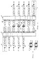
- FIG. 1 shows the circuit arrangement according to the invention with ten input modules and in Fig. 2 the possible connections of the circuit board connector are shown.
- the input modules 1 for the voltage signals all of which have the same structure, consist of a voltage converter 8, to which an adaptation circuit 9 is connected and which is followed by a low-pass filter 10.
- the input modules 2 for the current signals are also all constructed identically and consist of a current converter 11 which is connected on the secondary side to a current-voltage converter circuit 12 to which a low-pass filter 13 is connected.
- Two input modules 1 for the voltage signals and two input modules 2 for the current signals are each connected to two constant current sources 3 at the output.
- the constant current sources 3 of an input module 1, 2 are each connected to a microcomputer 4, 5.
- circuit board connectors 14 Three input modules 1 for the voltage signals and three input modules 2 for the current signals are connected to circuit board connectors 14.
- the four possible plug connections can be seen in FIG. 2.
- an input module 1, 2 can thus be connected to both microcomputers 4, 5, or the one input module 1 can be connected to one and the other input module 2 to the other microcomputer 4, 5 or vice versa.
- the circuit board connectors 14 are connected to the microcomputers 4, 5 via constant current sources 3. Since the circuit arrangement is usually arranged on a single circuit board, the connection is made for ease of service and for reasons of clarity realized between the constant current sources 3 and the microcomputers 4, 5 with ribbon cable 15.
Description
- Die Erfindung betrifft eine Schaltungsanordnung zur Aufbereitung von analogen Strom- und Spannungssignalen für die Weiterverarbeitung in Mikrocomputern.
- Bei modernen innovativen technischen Entwicklungen ist die Tendenz zu Systemlösungen eine allgemein übliche Erscheinung, so ist es heute gebräuchlich in Kraftwerken einen Systemschutz vorzusehen. Dieser vereint ein ganzes System von Einzelschutzfunktionen in einem einzigen Hard-bzw. Softwarekonzept. Eine höhere Integrationsdichte bezüglich Hardware, Software und funktionellen Verknüpfungen ist im Prinzip vielfach die einzige Möglichkeit wesentliche Verbesserungen zu erzielen.
- In der EP-A 0 283 889 ist ein Verarbeitungsmodul zur Erfassung analoger Eingangsgrößen, insbesondere für Mikroprozessorsysteme, beschrieben. Ein zugehöriger Programmspeicher wird vor dem Meßereignis programmiert, wodurch für jede Messung Halbleiterschalter entsprechend aktiviert werden. Bei diesem Verarbeitungsmodul kann jeder Eingang flexibel beschaltet werden und dient zur Aufnahme von Spannungsmeßwertgrößen, Strommeßwertgrößen oder zur Anpassung an Sensoren, wobei die Eingangskonfiguration nur durch Programmierung erfolgt. Ein Nachteil dieses Verarbeitungsmoduls ist, daß die an den Eingängen anstehenden Meßwerte nicht gleichzeitig erfaßt werden können, da die Abtastung der Eingänge seriell erfolgt. Zur Aufnahme von Meßwerten in Systemen, bei denen sich Abläufe rasch ändern, ist diese Schaltung daher nicht geeignet.
- Die Aufgabe der Erfindung besteht nun darin, eine Schaltungsanordnung zu schaffen, bei der die Anzahl der Ein- und Ausgänge für die Strom- und Spannungssignale variiert werden kann und dadurch eine Anpassung an die verschiedenen Anwendungsfälle einfach möglich ist.
- Die obige Aufgabe wird durch die Erfindung gelöst, welche dadurch gekennzeichnet ist, daß mindestens zwei Eingangsmodule für die Aufbereitung von Spannungssignalen und mindestens zwei Eingangsmodule für die Aufbereitung von Stromsignalen vorgesehen sind, von denen mindestens je ein Eingangsmodul über zwei Konstantstromquellen mit zwei Mikrocomputern verbunden ist, und daß am Ausgang der anderen Eingangsmodule je zwei lösbare Verbindungen angeordnet sind, die Leiterplattenstecker, einpolige Leiterplattenschalter z.B. Dual-in-line Schalter oder einpolige elektronische Schalter sind, über die entweder mindestens ein Eingangsmodul unter Zwischenschaltung von zwei Konstantstromquellen an beide Mikrocomputer anschließbar ist, oder mindestens je ein Eingangsmodul für die Spannungssignale mit dem einen Mikrocomputer und mindestens ein Eingangsmodul für die Stromsignale mit dem anderen Mikrocomputer über je eine Konstantstromquelle verbindbar ist, und daß die Anzahl der Eingänge bei beiden Mikrocomputern gleich ist, jedoch immer kleiner als die Anzahl aller Eingangsmodule, und daß die Anzahl der Konstantstromquellen der Summe der Eingänge bei beiden Mikrocomputern entspricht, und daß die Eingangsmodule, die lösbaren Verbindungen und die Konstantstromquellen auf einer Leiterplatte angeordnet sind. Die erfindungsgemäße Schaltung ist teilvariabel, d.h. bestimmte Eingangsmodule sind ausschließlich für Stromsignale oder für Spannungssignale vorgesehen. Die anderen Eingangsmodule können wahlweise über die lösbaren Verbindungen an die Mikrocomputer gelegt werden. Da die nicht variierbaren Eingangsmodule mit beiden Mikrocomputern verbunden sind werden auch die Redundanzanforderungen erfüllt. Es ist aber auch möglich mit den variablen Eingangsmodulen eine Redundanz zu erreichen. Durch die Konstantstromquellen werden Störeinflüsse und Übergangswiderstände eliminiert und es wird auch eine Langzeitkonstanz der Kalibrierung erreicht. Durch die Anordnung aller für die Schaltungsanordnung notwendigen Bauteile auf einer Leiterplatte ist die geforderte Kompaktheit gewährleistet. Da bei einem Defekt einzelner Eingangsmodule sofort die gesamte Leiterplatte ausgewechselt wird, ist auch eine große Servicefreundlichkeit der Schaltung gegeben.
- Nach einer Ausgestaltung der Erfindung bestehen die Eingangsmodule für die Spannungssignale aus einem Spannungswandler, einer diesem nachgeschalteten Anpassungsschaltung der ein Tiefpaßfilter folgt und die Eingangsmodule für die Stromsignale sind aus einem Stromwandler, an den eine Strom-Spannungswandlerschaltung mit Anpassung mit nachfolgendem Tiefpaßfilter angeschlossen ist, aufgebaut. Dies ist der einfachste und kostengünstigste Aufbau der Eingangsmodule.
- Von Vorteil ist weiters, daß an Stelle von jeweils vier lösbaren Verbindungen, wobei zwei von einem Eingangsmodul für die Spannungssignale und zwei von einem Eingangsmodul für die Stromsignale sind, ein zweipoliger vierstufiger Schalter vorgesehen ist, bei dem jeder Wurzelanschluß mit einer Konstantstromquelle verbunden ist, von denen jede mit einem Mikrocomputer verbunden ist, und daß in der ersten Schalterstellung der Eingangsmodul für die Spannungssignale mit beiden Mikrocomputern, in der zweiten Schalterstellung der Eingangsmodul für die Stromsignale mit beiden Mikrocomputern, in der dritten Schalterstellung der eine Eingangsmodul mit dem einen Mikrocomputer und der andere Eingangsmodul mit dem anderen Mikrocomputer und in der vierten Schalterstellung Eingangsmodule und Mikrocomputer in umgekehrter Reihenfolge miteinander verbunden ist bzw. sind. Mit dem Schalter erfolgt die Zuordnung der Eingangsmodule an die Mikrocomputer sehr einfach, da die vier Möglichkeiten bereits beim Schalter verdrahtet sind.
- Eine weitere Ausgestaltung der Erfindung liegt darin, daß die beiden Mikrocomputer über je ein Flachbandkabel mit mehrpoligen Steckern mit den Konstantstromquellen verbunden sind. Dies ist die übersichtlichste und einfachste Art zwei Schaltungen auf getrennten Printplatten mit mehreren Ein- und Ausgängen miteinander zu verbinden.
- Durch die Abstimmung der fixen und variablen Eingangsmodule auf die jeweilige Anforderung wird bei minimalem Hardwareeinsatz größtmögliche Freiheit beim Projektieren erreicht.
- An Hand der Zeichnungen wird die Erfindung nun noch näher erläutert. Das Blockschaltbild in Fig. 1 zeigt die erfindungsgemäße Schaltungsanordnung mit zehn Eingangsmodulen und in Fig. 2 sind die möglichen Verbindungen der Leiterplattenstecker dargestellt.
- In Fig. 1 sind fünf Eingangsmodule 1 für die Aufbereitung von Spannungssignalen und fünf Eingangsmodule 2 für die Aufbereitung von Stromsignalen dargestellt. Die Eingangsmodule 1 für die Spannungssignale, welche alle gleich aufgebaut sind, bestehen aus einem Spannungswandler 8, an den eine Anpassungsschaltung 9 angeschlossen ist und der ein Tiefpaßfilter 10 folgt. Die Eingangsmodule 2 für die Stromsignale sind ebenfalls alle gleich aufgebaut und bestehen aus einem Stromwandler 11, der sekundärseitig mit einer Strom-Spannungswandlerschaltung 12 verbunden ist, an die ein Tiefpaßfilter 13 angeschlossen ist. Zwei Eingangsmodule 1 für die Spannungssignale und zwei Eingangsmodule 2 für die Stromsignale sind am Ausgang mit je zwei Konstantstromquellen 3 verbunden. Die Konstantstromquellen 3 eines Eingangsmoduls 1, 2 sind an je einen Mikrocomputer 4, 5 angeschlossen.
Drei Eingangs module 1 für die Spannungssignale und drei Eingangsmodule 2 für die Stromsignale sind mit Leiterplattensteckern 14 verbunden. Die vier möglichen Steckverbindungen sind der Fig. 2 zu entnehmen. Wie hier ersichtlich ist, kann also ein Eingangsmodul 1, 2 an beide Mikrocomputer 4, 5 gelegt werden, oder der ein Eingangsmodul 1 an den einen und der andere Eingangsmodul 2 an den anderen Mikrocomputer 4, 5 oder umgekehrt angeschlossen werden.
Die Leiterplattenstecker 14 sind über Konstantstromquellen 3 mit den Mikrocomputern 4, 5 verbunden. Da die Schaltungsanordnung üblicherweise auf einer einzigen Leiterplatte angeordnet ist, wird zwecks Servicefreundlichkeit und aus Übersichtsgründen die Verbindung zwischen den Konstantstromquellen 3 und den Mikrocomputern 4, 5 mit Flachbandkabel 15 realisiert. - Entsprechend der Anforderung werden einige Eingangsmodule 1, 2 fix verdrahtet und bei den anderen kann die Verdrahtung über die Leiterplattenstecker 14 gewählt werden. Dadurch wird eine sehr große Flexibilität der Schaltung erreicht. Weiters wird auch die für einige Signale geforderte redundante Verarbeitung gewährleistet.
Claims (4)
- Schaltungsanordnung zur Aufbereitung von analogen Strom- und Spannungssignalen für die Weiterverarbeitung in Mikrocomputern, dadurch gekennzeichnet, daß mindestens zwei Eingangsmodule (1) für die Aufbereitung von Spannungssignalen und mindestens zwei Eingangsmodule (2) für die Aufbereitung von Stromsignalen vorgesehen sind, von denen mindestens je ein Eingangsmodul (1, 2) über zwei Konstantstromquellen (3) mit zwei Mikrocomputern (4, 5) verbunden ist, und daß am Ausgang der anderen Eingangsmodule (1, 2) je zwei lösbare Verbindungen (6, 7) angeordnet sind, die Leiterplattenstecker (14), einpolige Leiterplattenschalter z.B. Dual-in-line Schalter oder einpolige elektronische Schalter sind, über die entweder mindestens ein Eingangsmodul (1; 2) unter Zwischenschaltung von zwei Konstantstromquellen (3) an beide Mikrocomputer (4, 5) anschließbar ist, oder mindestens je ein Eingangsmodul (1) für die Spannungssignale mit dem einen Mikrocomputer (4) und mindestens ein Eingangsmodul (2) für die Stromsignale mit dem anderen Mikrocomputer (5) über je eine Konstantstromquelle (3) verbindbar ist, und daß die Anzahl der Eingänge bei beiden Mikrocomputern (4, 5) gleich ist, jedoch immer kleiner als die Anzahl aller Eingangsmodule (1, 2), und daß die Anzahl der Konstantstromquellen (3) der Summe der Eingänge bei beiden Mikrocomputern (4, 5) entspricht, und daß die Eingangsmodule (1, 2), die lösbaren Verbindungen (6, 7) und die Konstantstromquellen (3) auf einer Leiterplatte angeordnet sind.
- Schaltungsanordnung nach Anspruch 1, dadurch gekennzeichnet, daß die Eingangsmodule (1) für die Spannungssignale aus einem Spannungswandler (8), einer diesem nachgeschalteten Anpassungsschaltung (9) der ein Tiefpaßfilter (10) folgt, besteht, und daß die Eingangsmodule (2) für die Stromsignale aus einem Stromwandler (11), an den eine Strom-Spannungswandlerschaltung 12 mit Anpassung mit nachfolgendem Tiefpaßfilter (13) angeschlossen ist, aufgebaut sind.
- Schaltungsanordnung nach Anspruch 1 oder 2, dadurch gekennzeichnet, daß an Stelle von jeweils vier lösbaren Verbindungen (6, 7), wobei zwei von einem Eingangsmodul (1) für die Spannungssignale und zwei von einem Eingangsmodul (2) für die Stromsignale sind, ein zweipoliger vierstufiger Schalter vorgesehen ist, bei dem jeder Wurzelanschluß mit einer Konstantstromquelle (3) verbunden ist, von denen jede mit einem Mikrocomputer (4, 5) verbunden ist, und daß in der ersten Schalterstellung der Eingangsmodul (1) für die Spannungssignale mit beiden Mikrocomputern (4, 5), in der zweiten Schalterstellung der Eingangsmodul (2) für die Stromsignale mit beiden Mikrocomputern (4, 5), in der dritten Schalterstellung der eine Eingangsmodul (1) mit dem einen Mikrocomputer (4) und der andere Eingangsmodul (2) mit dem anderen Mikrocomputer (5) und in der vierten Schalterstellung Eingangsmodule (1, 2) und Mikrocomputer (4, 5) in umgekehrter Reihenfolge miteinander verbunden ist bzw. sind.
- Schaltungsanordnung nach einem der Ansprüche 1 bis 3, dadurch gekennzeichnet, daß die beiden Mikrocomputer (4, 5) über je ein Flachbandkabel (15) mit mehrpoligen Steckern mit den Konstantstromquellen (3) verbunden sind.
Applications Claiming Priority (3)
| Application Number | Priority Date | Filing Date | Title |
|---|---|---|---|
| AT2272/92 | 1992-11-17 | ||
| AT0227292A AT402459B (de) | 1992-11-17 | 1992-11-17 | Schaltungsanordnung zur aufbereitung von analogen strom- und spannungssignalen |
| PCT/AT1993/000175 WO1994011707A1 (de) | 1992-11-17 | 1993-11-17 | Schaltungsanordnung zur aufbereitung von analogen strom- und spannungssignalen |
Publications (2)
| Publication Number | Publication Date |
|---|---|
| EP0670033A1 EP0670033A1 (de) | 1995-09-06 |
| EP0670033B1 true EP0670033B1 (de) | 1997-01-15 |
Family
ID=3531267
Family Applications (1)
| Application Number | Title | Priority Date | Filing Date |
|---|---|---|---|
| EP93924428A Expired - Lifetime EP0670033B1 (de) | 1992-11-17 | 1993-11-17 | Schaltungsanordnung zur aufbereitung von analogen strom- und spannungssignalen |
Country Status (7)
| Country | Link |
|---|---|
| EP (1) | EP0670033B1 (de) |
| CN (1) | CN1044405C (de) |
| AT (2) | AT402459B (de) |
| DE (1) | DE59305182D1 (de) |
| FI (1) | FI952374A0 (de) |
| NO (1) | NO311108B1 (de) |
| WO (1) | WO1994011707A1 (de) |
Families Citing this family (3)
| Publication number | Priority date | Publication date | Assignee | Title |
|---|---|---|---|---|
| DE19719633C2 (de) * | 1997-05-09 | 2000-03-30 | Daimler Chrysler Ag | Meßwertaufbereitungssystem |
| DE10100381C2 (de) * | 2001-01-05 | 2002-12-12 | Man B & W Diesel Ag | Klemmbox für einen Sensoranschluß innerhalb eines Anschlußkonzepts für Meßverstärker |
| CN115420940B (zh) * | 2022-11-04 | 2023-03-03 | 山东恒美电子科技有限公司 | 一种多用途的直流信号检测系统 |
Family Cites Families (4)
| Publication number | Priority date | Publication date | Assignee | Title |
|---|---|---|---|---|
| US4278940A (en) * | 1979-04-25 | 1981-07-14 | General Electric Company | Means for automatically compensating DC magnetization in a transformer |
| JPS6252870A (ja) * | 1985-08-30 | 1987-03-07 | デユポン ジヤパン リミテツド | 短絡コネクタ |
| US4711757A (en) * | 1986-02-27 | 1987-12-08 | Westinghouse Electric Corp. | Position indicating device |
| DE3709805A1 (de) * | 1987-03-25 | 1988-10-13 | Kloeckner Moeller Elektrizit | Verarbeitungsmodul zur erfassung analoger eingangsgroessen, insbesondere fuer mikroprozessorsysteme und speicherprogrammierbare steuerungen |
-
1992
- 1992-11-17 AT AT0227292A patent/AT402459B/de not_active IP Right Cessation
-
1993
- 1993-11-17 WO PCT/AT1993/000175 patent/WO1994011707A1/de active IP Right Grant
- 1993-11-17 CN CN93120543A patent/CN1044405C/zh not_active Expired - Fee Related
- 1993-11-17 AT AT93924428T patent/ATE147851T1/de not_active IP Right Cessation
- 1993-11-17 DE DE59305182T patent/DE59305182D1/de not_active Expired - Fee Related
- 1993-11-17 EP EP93924428A patent/EP0670033B1/de not_active Expired - Lifetime
-
1995
- 1995-05-16 NO NO19951938A patent/NO311108B1/no not_active IP Right Cessation
- 1995-05-16 FI FI952374A patent/FI952374A0/fi unknown
Also Published As
| Publication number | Publication date |
|---|---|
| NO951938L (no) | 1995-05-16 |
| CN1091213A (zh) | 1994-08-24 |
| DE59305182D1 (de) | 1997-02-27 |
| NO311108B1 (no) | 2001-10-08 |
| ATE147851T1 (de) | 1997-02-15 |
| FI952374A (fi) | 1995-05-16 |
| AT402459B (de) | 1997-05-26 |
| FI952374A0 (fi) | 1995-05-16 |
| WO1994011707A1 (de) | 1994-05-26 |
| ATA227292A (de) | 1996-09-15 |
| NO951938D0 (no) | 1995-05-16 |
| EP0670033A1 (de) | 1995-09-06 |
| CN1044405C (zh) | 1999-07-28 |
Similar Documents
| Publication | Publication Date | Title |
|---|---|---|
| EP0712267B1 (de) | Modulare Steuerungsanlage mit integriertem Feldbusanschluss | |
| DE3805593A1 (de) | Tasteneingabevorrichtung | |
| DE3510820C2 (de) | ||
| CH640938A5 (de) | Elektronisches geraet nach dem baukastenprinzip zur verarbeitung einer mehrzahl von simultanen messsignalen, insbesondere zur verwendung bei der ueberpruefung von geometrischen abmessungen. | |
| DE2717372C3 (de) | Baugruppe aus einem Digitalschalter und elektronischen Bauelementen | |
| DE2547323C3 (de) | Trägerplatte für wenigstens eine integrierte Halbleitershaltung | |
| EP0670033B1 (de) | Schaltungsanordnung zur aufbereitung von analogen strom- und spannungssignalen | |
| EP0939976B1 (de) | Einrichtung zur codierung von steckplätzen | |
| DE4032370A1 (de) | Schaltungsanordnung mit wenigstens zwei identischen, integrierten schaltungen oder schaltungsmodulen | |
| DE4223193A1 (de) | Programmierbare Steuerung mit Anschlußeinheiten zur Verbindung mit analogen und/oder digitalen Peripheriegeräten | |
| DE4013815C2 (de) | Steuerschaltung für Maschinen | |
| EP0249907B1 (de) | Gehäusesystem für elektrische Geräte | |
| EP0142182B1 (de) | Schaltungsanordnung zum Umwandeln eines digitalen Eingangssignals in ein analoges Ausgangssignal | |
| DE3008262C2 (de) | Elektronische Schaltungsanordnung | |
| EP0940066B1 (de) | Einrichtung zur codierung von steckbaugruppen sowie einrichtung zum anschluss externer leitungen mit einer derartigen codiereinrichtung | |
| EP0888707B1 (de) | Baugruppe mit einer schaltungsanordnung | |
| EP0177804B1 (de) | Stromspeiseschaltung für ein Digitalisiertablett | |
| EP0740235B1 (de) | Peripheriesystem | |
| DE4413457C2 (de) | Anschlußeinheit eines Automatisierungssystems und hierzu korrespondierender Klemmenblock | |
| DE3641528C2 (de) | ||
| DE3011564C2 (de) | Programmträger zum Programmieren von Steuerfunktionen | |
| DE3120640C2 (de) | ||
| DE2154275A1 (de) | Einrichtung zur spannungsversorgung | |
| DE2947407A1 (de) | Vorrichtung zur informationseingabe bzw. erzeugung eines codes | |
| DE1238516B (de) | In einer Ebene aufgebaute und aus mehreren Teilplatten mechanisch zusammengesetzte gedruckte Schaltung |
Legal Events
| Date | Code | Title | Description |
|---|---|---|---|
| PUAI | Public reference made under article 153(3) epc to a published international application that has entered the european phase |
Free format text: ORIGINAL CODE: 0009012 |
|
| 17P | Request for examination filed |
Effective date: 19950413 |
|
| AK | Designated contracting states |
Kind code of ref document: A1 Designated state(s): AT CH DE ES FR IT LI SE |
|
| GRAG | Despatch of communication of intention to grant |
Free format text: ORIGINAL CODE: EPIDOS AGRA |
|
| 17Q | First examination report despatched |
Effective date: 19960326 |
|
| GRAH | Despatch of communication of intention to grant a patent |
Free format text: ORIGINAL CODE: EPIDOS IGRA |
|
| GRAH | Despatch of communication of intention to grant a patent |
Free format text: ORIGINAL CODE: EPIDOS IGRA |
|
| GRAA | (expected) grant |
Free format text: ORIGINAL CODE: 0009210 |
|
| AK | Designated contracting states |
Kind code of ref document: B1 Designated state(s): AT CH DE ES FR IT LI SE |
|
| PG25 | Lapsed in a contracting state [announced via postgrant information from national office to epo] |
Ref country code: IT Free format text: LAPSE BECAUSE OF FAILURE TO SUBMIT A TRANSLATION OF THE DESCRIPTION OR TO PAY THE FEE WITHIN THE PRESCRIBED TIME-LIMIT;WARNING: LAPSES OF ITALIAN PATENTS WITH EFFECTIVE DATE BEFORE 2007 MAY HAVE OCCURRED AT ANY TIME BEFORE 2007. THE CORRECT EFFECTIVE DATE MAY BE DIFFERENT FROM THE ONE RECORDED. Effective date: 19970115 Ref country code: FR Effective date: 19970115 Ref country code: ES Free format text: THE PATENT HAS BEEN ANNULLED BY A DECISION OF A NATIONAL AUTHORITY Effective date: 19970115 |
|
| REF | Corresponds to: |
Ref document number: 147851 Country of ref document: AT Date of ref document: 19970215 Kind code of ref document: T |
|
| REG | Reference to a national code |
Ref country code: CH Ref legal event code: EP |
|
| REF | Corresponds to: |
Ref document number: 59305182 Country of ref document: DE Date of ref document: 19970227 |
|
| EN | Fr: translation not filed | ||
| PLBE | No opposition filed within time limit |
Free format text: ORIGINAL CODE: 0009261 |
|
| STAA | Information on the status of an ep patent application or granted ep patent |
Free format text: STATUS: NO OPPOSITION FILED WITHIN TIME LIMIT |
|
| 26N | No opposition filed | ||
| PGFP | Annual fee paid to national office [announced via postgrant information from national office to epo] |
Ref country code: SE Payment date: 20001030 Year of fee payment: 8 |
|
| PG25 | Lapsed in a contracting state [announced via postgrant information from national office to epo] |
Ref country code: SE Free format text: LAPSE BECAUSE OF NON-PAYMENT OF DUE FEES Effective date: 20011118 |
|
| EUG | Se: european patent has lapsed |
Ref document number: 93924428.1 |
|
| PGFP | Annual fee paid to national office [announced via postgrant information from national office to epo] |
Ref country code: DE Payment date: 20021024 Year of fee payment: 10 |
|
| PGFP | Annual fee paid to national office [announced via postgrant information from national office to epo] |
Ref country code: CH Payment date: 20021028 Year of fee payment: 10 |
|
| PGFP | Annual fee paid to national office [announced via postgrant information from national office to epo] |
Ref country code: AT Payment date: 20021029 Year of fee payment: 10 |
|
| PG25 | Lapsed in a contracting state [announced via postgrant information from national office to epo] |
Ref country code: AT Free format text: LAPSE BECAUSE OF NON-PAYMENT OF DUE FEES Effective date: 20031117 |
|
| PG25 | Lapsed in a contracting state [announced via postgrant information from national office to epo] |
Ref country code: LI Free format text: LAPSE BECAUSE OF NON-PAYMENT OF DUE FEES Effective date: 20031130 Ref country code: CH Free format text: LAPSE BECAUSE OF NON-PAYMENT OF DUE FEES Effective date: 20031130 |
|
| PG25 | Lapsed in a contracting state [announced via postgrant information from national office to epo] |
Ref country code: DE Free format text: LAPSE BECAUSE OF NON-PAYMENT OF DUE FEES Effective date: 20040602 |
|
| REG | Reference to a national code |
Ref country code: CH Ref legal event code: PL |