EP0660415B1 - Kaskadierte Hochspannungsnetzwerkschaltung - Google Patents
Kaskadierte Hochspannungsnetzwerkschaltung Download PDFInfo
- Publication number
- EP0660415B1 EP0660415B1 EP94120205A EP94120205A EP0660415B1 EP 0660415 B1 EP0660415 B1 EP 0660415B1 EP 94120205 A EP94120205 A EP 94120205A EP 94120205 A EP94120205 A EP 94120205A EP 0660415 B1 EP0660415 B1 EP 0660415B1
- Authority
- EP
- European Patent Office
- Prior art keywords
- high voltage
- resistor
- terminal
- drain
- gate
- Prior art date
- Legal status (The legal status is an assumption and is not a legal conclusion. Google has not performed a legal analysis and makes no representation as to the accuracy of the status listed.)
- Expired - Lifetime
Links
Images




Classifications
-
- H—ELECTRICITY
- H03—ELECTRONIC CIRCUITRY
- H03K—PULSE TECHNIQUE
- H03K17/00—Electronic switching or gating, i.e. not by contact-making and –breaking
- H03K17/10—Modifications for increasing the maximum permissible switched voltage
- H03K17/102—Modifications for increasing the maximum permissible switched voltage in field-effect transistor switches
-
- H—ELECTRICITY
- H10—SEMICONDUCTOR DEVICES; ELECTRIC SOLID-STATE DEVICES NOT OTHERWISE PROVIDED FOR
- H10D—INORGANIC ELECTRIC SEMICONDUCTOR DEVICES
- H10D30/00—Field-effect transistors [FET]
- H10D30/60—Insulated-gate field-effect transistors [IGFET]
- H10D30/64—Double-diffused metal-oxide semiconductor [DMOS] FETs
- H10D30/65—Lateral DMOS [LDMOS] FETs
-
- H—ELECTRICITY
- H10—SEMICONDUCTOR DEVICES; ELECTRIC SOLID-STATE DEVICES NOT OTHERWISE PROVIDED FOR
- H10D—INORGANIC ELECTRIC SEMICONDUCTOR DEVICES
- H10D64/00—Electrodes of devices having potential barriers
- H10D64/111—Field plates
- H10D64/115—Resistive field plates, e.g. semi-insulating field plates
-
- H—ELECTRICITY
- H10—SEMICONDUCTOR DEVICES; ELECTRIC SOLID-STATE DEVICES NOT OTHERWISE PROVIDED FOR
- H10W—GENERIC PACKAGES, INTERCONNECTIONS, CONNECTORS OR OTHER CONSTRUCTIONAL DETAILS OF DEVICES COVERED BY CLASS H10
- H10W20/00—Interconnections in chips, wafers or substrates
- H10W20/40—Interconnections external to wafers or substrates, e.g. back-end-of-line [BEOL] metallisations or vias connecting to gate electrodes
- H10W20/482—Interconnections external to wafers or substrates, e.g. back-end-of-line [BEOL] metallisations or vias connecting to gate electrodes for individual devices provided for in groups H10D8/00 - H10D48/00, e.g. for power transistors
- H10W20/484—Interconnections having extended contours, e.g. pads having mesh shape or interconnections comprising connected parallel stripes
Definitions
- a special high voltage MOS device is described in US-A-4 288 806. It comprises source, drain and gate regions with corresponding terminals. Connected to the gate and its terminal is a resistor with a corresponding terminal. This device, therefore, is a four terminal device.
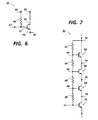
- Figure 6 is a high voltage NMOS device for use in a cascaded network according to the present invention.
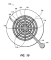
- the fingers 118 have a wide inward end 122 and a narrow outward end 124.
- Designing a field plate using a series of concentric rings 120 connected with radial fingers 118 facilitates a field plate with the advantages of both spiral field plates, as shown in Figure 8 and ring field plates, as shown in Figure 9.
- the wide inward end 122 of the fingers 118 provides a physically larger connection between the fingers 118 and the rings 120 where the voltage concentration is the largest. This allows the field plate 116 to more effectively space the equipotential lines.
- the narrow outward end 124 of the fingers 118 provides a physically smaller connection where the voltage concentration is the smallest. For most efficient operation, the ratio of the width of the wide inward end 122 to the width of the narrow outward end 124 should be approximately 2:1.
- the rings 120 can be constructed out of a medium resistance polysilicon, typically having values of 10 kilo ohms per square.
- the rings 120 are fabricated using the same techniques and materials used to produce the spaced concentric rings 104 shown in the high voltage NMOS device 100 in Figure 9. It is this feature which facilitates production of very high ohmic resistors. Typical values range from 150 mega ohms to 10 giga ohms.
Landscapes
- Semiconductor Integrated Circuits (AREA)
- Insulated Gate Type Field-Effect Transistor (AREA)
- Metal-Oxide And Bipolar Metal-Oxide Semiconductor Integrated Circuits (AREA)
Claims (1)
- Eine kaskadierte Hochspannungsnetzwerkschaltung, die folgendes umfaßt:a) einen elektrischen Schaltkreis (62) von zumindest zwei Hochspannungstransistoren (50,64,66,68,70,100,114) mit je vier Anschlüssen, die in einem Kaskadenaufbau von einem ersten Transistor (70) zu einem letzten Transistor (64) verbunden sind, wobei jeder Transistor folgendes umfaßt:wobei die kaskadierte Hochspannungsnetzwerkschaltung weiterhin folgendes umfaßt:i) einen Sourcebereich, einen Drainbereich, einen Gatebereich und einen Widerstandsbereich,ii) wobei all diese Bereiche in einem konzentrischen Aufbau angeordnet sind, der Drainbereich der innerste Bereich ist, der Widerstandsbereich den Drainbereich umgibt, der Gatebereich den Widerstandsbereich umgibt und der Sourcebereich den Gatebereich umgibt,iii) eine Source (56), die einen Sourceanschluß (57) hat, wobei die Source in dem Sourcebereich angeordnet ist,iv) eine Drain (54,108), die einen Drainanschluß (55) hat, wobei die Drain in dem Drainbereich angeordnet ist,v) ein Gate (52), das einen Gateanschluß (53) hat, wobei das Gate in dem Gatebereich angeordnet ist,vi) einen Widerstandsanschluß (60), undvii) ein Widerstandselement (58,86,88,90,92), das zwei Enden hat, wobei das Widerstandselement in dem Widerstandsbereich angeordnet ist und ein Ende des Widerstandselementes elektrisch mit dem Gateanschluß (53) verbunden ist und das andere Ende des Widerstandselementes elektrisch mit dem Widerstandsanschluß (60) verbunden ist, wobei das Widerstandselement eine Feldplattenelektrode für den Transistor bildet,b) einen positiven Knoten (72),c) einen negativen Knoten,d) wobei der Sourceanschluß des ersten Transistors (70) mit dem negativen Knoten verbunden ist,e) der Widerstandsanschluß und der Drainanschluß der Drain des letzten Transistors (64) mit dem positiven Knoten (72) verbunden sind, undf) jeder der Transistoren, der nicht der letzte Transistor (64) ist,i) seinen Drainanschluß elektrisch mit dem Sourceanschluß des folgenden Transistors in der Kaskade (62) verbunden hat,ii) seinen Widerstandsanschluß elektrisch mit dem Gateanschluß des folgenden Transistors in der Kaskade (62) verbunden hat,g) jeder der Transistoren, der nicht der erste Transistor (70) ist,i) seinen Sourceanschluß elektrisch mit dem Drainanschluß des vorausgehenden Transistors in der Kaskade (62) verbunden hat, undii) seinen Gateanschluß elektrisch mit dem Widerstandsanschluß des vorausgehenden Transistors in der Kaskade (62) verbunden hat.
Applications Claiming Priority (2)
| Application Number | Priority Date | Filing Date | Title |
|---|---|---|---|
| US08/170,848 US5382826A (en) | 1993-12-21 | 1993-12-21 | Stacked high voltage transistor unit |
| US170848 | 1993-12-21 |
Publications (2)
| Publication Number | Publication Date |
|---|---|
| EP0660415A1 EP0660415A1 (de) | 1995-06-28 |
| EP0660415B1 true EP0660415B1 (de) | 1999-03-17 |
Family
ID=22621514
Family Applications (1)
| Application Number | Title | Priority Date | Filing Date |
|---|---|---|---|
| EP94120205A Expired - Lifetime EP0660415B1 (de) | 1993-12-21 | 1994-12-20 | Kaskadierte Hochspannungsnetzwerkschaltung |
Country Status (4)
| Country | Link |
|---|---|
| US (1) | US5382826A (de) |
| EP (1) | EP0660415B1 (de) |
| JP (1) | JPH07202004A (de) |
| DE (1) | DE69417189T2 (de) |
Families Citing this family (53)
| Publication number | Priority date | Publication date | Assignee | Title |
|---|---|---|---|---|
| JPH05283702A (ja) * | 1992-04-03 | 1993-10-29 | Hitachi Ltd | 複合制御型半導体装置及びそれを使用した電力変換装置 |
| US5486718A (en) * | 1994-07-05 | 1996-01-23 | Motorola, Inc. | High voltage planar edge termination structure and method of making same |
| US5600149A (en) * | 1995-10-30 | 1997-02-04 | Xerox Corporation | Power supply regulator |
| US5936874A (en) | 1997-06-19 | 1999-08-10 | Micron Technology, Inc. | High density semiconductor memory and method of making |
| DE69832258T2 (de) | 1998-02-24 | 2006-08-03 | Stmicroelectronics S.R.L., Agrate Brianza | Schutzstruktur für integrierte elektronische Hochspannungsanordnungen |
| US5918137A (en) * | 1998-04-27 | 1999-06-29 | Spectrian, Inc. | MOS transistor with shield coplanar with gate electrode |
| US6680515B1 (en) * | 2000-11-10 | 2004-01-20 | Monolithic Power Systems, Inc. | Lateral high voltage transistor having spiral field plate and graded concentration doping |
| US20040201078A1 (en) * | 2003-04-11 | 2004-10-14 | Liping Ren | Field plate structure for high voltage devices |
| SE0302810D0 (sv) * | 2003-10-24 | 2003-10-24 | Infineon Technologies Ag | Monolithically integrated circuit comprising a thin film resistor, and fabrication method thereof |
| JP5395137B2 (ja) * | 2004-02-24 | 2014-01-22 | セイコーインスツル株式会社 | 高電圧動作電界効果トランジスタとそのバイアス回路およびその高電圧動作回路要素 |
| DE102004019345B4 (de) * | 2004-04-21 | 2007-02-08 | Austriamicrosystems Ag | Ausgangsstufenanordnung |
| US20050274985A1 (en) * | 2004-05-26 | 2005-12-15 | Adlerstein Michael G | RF decoupled field plate for FETs |
| DE102004039620B4 (de) * | 2004-08-06 | 2006-10-12 | Atmel Germany Gmbh | Integrierte Schaltung, die eine vorgegebene Spannungsfestigkeit besitzt |
| US7183626B2 (en) * | 2004-11-17 | 2007-02-27 | International Rectifier Corporation | Passivation structure with voltage equalizing loops |
| US7498651B2 (en) * | 2004-11-24 | 2009-03-03 | Microsemi Corporation | Junction termination structures for wide-bandgap power devices |
| US7955943B2 (en) * | 2005-01-25 | 2011-06-07 | Semiconductor Components Industries, Llc | High voltage sensor device and method therefor |
| US7709292B2 (en) * | 2006-09-29 | 2010-05-04 | Sadwick Laurence P | Processes and packaging for high voltage integrated circuits, electronic devices, and circuits |
| US7782644B2 (en) * | 2007-03-03 | 2010-08-24 | Sadwick Laurence P | Method and apparatus for supplying power |
| US8009452B1 (en) | 2007-03-03 | 2011-08-30 | Sadwick Laurence P | Multiple driver power supply |
| US7709908B2 (en) * | 2007-08-10 | 2010-05-04 | United Microelectronics Corp. | High-voltage MOS transistor device |
| EP2293445B1 (de) * | 2009-08-26 | 2013-03-06 | The Alfred E. Mann Foundation for Scientific Research | Hochspannungsstromquelle und Spannungserweiterer in einem Niederspannungsprozess |
| US8289054B2 (en) * | 2009-08-26 | 2012-10-16 | Alfred E. Mann Foundation For Scientific Research | High voltage differential pair and op amp in low voltage process |
| US8461903B1 (en) | 2009-09-11 | 2013-06-11 | Rf Micro Devices, Inc. | SOI switch enhancement |
| US20110062554A1 (en) * | 2009-09-17 | 2011-03-17 | Hsing Michael R | High voltage floating well in a silicon die |
| US8598637B2 (en) * | 2009-09-18 | 2013-12-03 | Monolithic Power Systems, Inc. | High voltage junction field effect transistor with spiral field plate |
| TWI503956B (zh) * | 2009-09-30 | 2015-10-11 | Semiconductor Components Ind | 高電壓感測器設備及其方法 |
| US8587073B2 (en) * | 2010-10-15 | 2013-11-19 | Taiwan Semiconductor Manufacturing Company, Ltd. | High voltage resistor |
| US8786050B2 (en) | 2011-05-04 | 2014-07-22 | Taiwan Semiconductor Manufacturing Company, Ltd. | High voltage resistor with biased-well |
| US8664741B2 (en) | 2011-06-14 | 2014-03-04 | Taiwan Semiconductor Manufacturing Company Ltd. | High voltage resistor with pin diode isolation |
| US9373619B2 (en) | 2011-08-01 | 2016-06-21 | Taiwan Semiconductor Manufacturing Company, Ltd. | High voltage resistor with high voltage junction termination |
| US20130161740A1 (en) * | 2011-12-21 | 2013-06-27 | Donald R. Disney | Lateral High-Voltage Transistor with Buried Resurf Layer and Associated Method for Manufacturing the Same |
| US8766357B2 (en) | 2012-03-01 | 2014-07-01 | Taiwan Semiconductor Manufacturing Company, Ltd. | Apparatus and method for high voltage MOS transistor |
| US10147724B2 (en) | 2012-07-07 | 2018-12-04 | Skyworks Solutions, Inc. | Feed-forward circuit to improve intermodulation distortion performance of radio-frequency switch |
| US9059702B2 (en) | 2012-07-07 | 2015-06-16 | Skyworks Solutions, Inc. | Switch linearization by non-linear compensation of a field-effect transistor |
| US9148194B2 (en) | 2012-07-07 | 2015-09-29 | Skyworks Solutions, Inc. | Radio-frequency switch system having improved intermodulation distortion performance |
| US8975950B2 (en) | 2012-07-07 | 2015-03-10 | Skyworks Solutions, Inc. | Switching device having a discharge circuit for improved intermodulation distortion performance |
| US9628075B2 (en) | 2012-07-07 | 2017-04-18 | Skyworks Solutions, Inc. | Radio-frequency switch having dynamic body coupling |
| US9276570B2 (en) | 2012-07-07 | 2016-03-01 | Skyworks Solutions, Inc. | Radio-frequency switch having gate node voltage compensation network |
| US9160328B2 (en) | 2012-07-07 | 2015-10-13 | Skyworks Solutions, Inc. | Circuits, devices, methods and applications related to silicon-on-insulator based radio-frequency switches |
| JP2014017962A (ja) * | 2012-07-09 | 2014-01-30 | Denso Corp | 起動回路付半導体装置 |
| CN103579313A (zh) * | 2012-08-10 | 2014-02-12 | 上海华虹Nec电子有限公司 | 提高高压ldmos器件击穿电压的结构 |
| JP2014063771A (ja) * | 2012-09-19 | 2014-04-10 | Toshiba Corp | 半導体装置 |
| US9013225B2 (en) | 2013-02-04 | 2015-04-21 | Skyworks Solutions, Inc. | RF switches having increased voltage swing uniformity |
| US8786397B1 (en) * | 2013-02-07 | 2014-07-22 | Excelliance Mos Corporation | Electric field resistor |
| CN103219898B (zh) * | 2013-04-02 | 2016-06-01 | 苏州博创集成电路设计有限公司 | 具有电流采样和启动结构的半导体装置 |
| US9948281B2 (en) | 2016-09-02 | 2018-04-17 | Peregrine Semiconductor Corporation | Positive logic digitally tunable capacitor |
| US10608623B2 (en) | 2016-12-21 | 2020-03-31 | Qorvo US. Inc. | Transistor-based radio frequency (RF) switch |
| US10320379B2 (en) | 2016-12-21 | 2019-06-11 | Qorvo Us, Inc. | Transistor-based radio frequency (RF) switch |
| DE102017130213B4 (de) * | 2017-12-15 | 2021-10-21 | Infineon Technologies Ag | Planarer feldeffekttransistor |
| US10505530B2 (en) | 2018-03-28 | 2019-12-10 | Psemi Corporation | Positive logic switch with selectable DC blocking circuit |
| US10236872B1 (en) | 2018-03-28 | 2019-03-19 | Psemi Corporation | AC coupling modules for bias ladders |
| US10886911B2 (en) | 2018-03-28 | 2021-01-05 | Psemi Corporation | Stacked FET switch bias ladders |
| US11476849B2 (en) | 2020-01-06 | 2022-10-18 | Psemi Corporation | High power positive logic switch |
Family Cites Families (3)
| Publication number | Priority date | Publication date | Assignee | Title |
|---|---|---|---|---|
| BE785747A (fr) * | 1971-07-02 | 1973-01-02 | Philips Nv | Dispositif semiconducteur |
| US4333225A (en) * | 1978-12-18 | 1982-06-08 | Xerox Corporation | Method of making a circular high voltage field effect transistor |
| US4288806A (en) * | 1979-05-29 | 1981-09-08 | Xerox Corporation | High voltage MOSFET with overlapping electrode structure |
-
1993
- 1993-12-21 US US08/170,848 patent/US5382826A/en not_active Expired - Lifetime
-
1994
- 1994-12-19 JP JP6315340A patent/JPH07202004A/ja active Pending
- 1994-12-20 DE DE69417189T patent/DE69417189T2/de not_active Expired - Fee Related
- 1994-12-20 EP EP94120205A patent/EP0660415B1/de not_active Expired - Lifetime
Also Published As
| Publication number | Publication date |
|---|---|
| DE69417189T2 (de) | 1999-07-08 |
| EP0660415A1 (de) | 1995-06-28 |
| JPH07202004A (ja) | 1995-08-04 |
| DE69417189D1 (de) | 1999-04-22 |
| US5382826A (en) | 1995-01-17 |
Similar Documents
| Publication | Publication Date | Title |
|---|---|---|
| EP0660415B1 (de) | Kaskadierte Hochspannungsnetzwerkschaltung | |
| JP3278443B2 (ja) | ユーザ構成可能な相互接続アーキテクチャ | |
| JP3566512B2 (ja) | 静電気保護回路 | |
| KR960003858B1 (ko) | 보호 소자를 갖고 있는 반도체 집적 회로 | |
| US20190378793A1 (en) | Integration of guard ring with passive components | |
| US20070267733A1 (en) | Symmetrical MIMCAP capacitor design | |
| US20040056756A1 (en) | Impedance network with minimum contact impedance | |
| US6570435B1 (en) | Integrated circuit with current limited charge pump and method | |
| JP3043250B2 (ja) | ゲートアレイ用アナログ出力駆動回路 | |
| US9660019B2 (en) | Concentric capacitor structure | |
| JPH0455342B2 (de) | ||
| US20060208287A1 (en) | Lateral Programmable Polysilicon Structure Incorporating Polysilicon Blocking Diode | |
| EP0658942A2 (de) | Vertikaler PMOS-Transistor für hohe Ströme und hohe Spannungen | |
| KR20020062162A (ko) | 복수의 다이오드를 케스케이드 접속하여 이루어진 반도체장치 | |
| US3999205A (en) | Rectifier structure for a semiconductor integrated circuit device | |
| US3544860A (en) | Integrated power output circuit | |
| US20040016960A1 (en) | Integrated capacitor for sensing the voltage applied to a terminal of an integrated or discrete power device on a semiconductor substrate | |
| US20050067657A1 (en) | Semiconductor device | |
| JP3450408B2 (ja) | Lc複合素子 | |
| EP0466176A1 (de) | Integrierte Halbleiterschaltungsanordnung mit Verbindungsmaterial | |
| US12501717B2 (en) | Semiconductor structure with a gate and a shielding structure | |
| TWI847365B (zh) | 半導體裝置及其布局方法 | |
| JPS61501296A (ja) | 集積半導体構造 | |
| KR100283972B1 (ko) | 반도체 집적 회로 | |
| US6903620B2 (en) | Circuit configuration for setting the input resistance and the input capacitance of an integrated semiconductor circuit chip |
Legal Events
| Date | Code | Title | Description |
|---|---|---|---|
| PUAI | Public reference made under article 153(3) epc to a published international application that has entered the european phase |
Free format text: ORIGINAL CODE: 0009012 |
|
| AK | Designated contracting states |
Kind code of ref document: A1 Designated state(s): DE FR GB |
|
| 17P | Request for examination filed |
Effective date: 19951227 |
|
| 17Q | First examination report despatched |
Effective date: 19961203 |
|
| GRAG | Despatch of communication of intention to grant |
Free format text: ORIGINAL CODE: EPIDOS AGRA |
|
| GRAG | Despatch of communication of intention to grant |
Free format text: ORIGINAL CODE: EPIDOS AGRA |
|
| GRAH | Despatch of communication of intention to grant a patent |
Free format text: ORIGINAL CODE: EPIDOS IGRA |
|
| GRAH | Despatch of communication of intention to grant a patent |
Free format text: ORIGINAL CODE: EPIDOS IGRA |
|
| GRAA | (expected) grant |
Free format text: ORIGINAL CODE: 0009210 |
|
| AK | Designated contracting states |
Kind code of ref document: B1 Designated state(s): DE FR GB |
|
| REF | Corresponds to: |
Ref document number: 69417189 Country of ref document: DE Date of ref document: 19990422 |
|
| ET | Fr: translation filed | ||
| PLBE | No opposition filed within time limit |
Free format text: ORIGINAL CODE: 0009261 |
|
| STAA | Information on the status of an ep patent application or granted ep patent |
Free format text: STATUS: NO OPPOSITION FILED WITHIN TIME LIMIT |
|
| 26N | No opposition filed | ||
| REG | Reference to a national code |
Ref country code: GB Ref legal event code: IF02 |
|
| PGFP | Annual fee paid to national office [announced via postgrant information from national office to epo] |
Ref country code: FR Payment date: 20021210 Year of fee payment: 9 |
|
| PGFP | Annual fee paid to national office [announced via postgrant information from national office to epo] |
Ref country code: GB Payment date: 20021218 Year of fee payment: 9 |
|
| PGFP | Annual fee paid to national office [announced via postgrant information from national office to epo] |
Ref country code: DE Payment date: 20021231 Year of fee payment: 9 |
|
| PG25 | Lapsed in a contracting state [announced via postgrant information from national office to epo] |
Ref country code: GB Free format text: LAPSE BECAUSE OF NON-PAYMENT OF DUE FEES Effective date: 20031220 |
|
| PG25 | Lapsed in a contracting state [announced via postgrant information from national office to epo] |
Ref country code: DE Free format text: LAPSE BECAUSE OF NON-PAYMENT OF DUE FEES Effective date: 20040701 |
|
| GBPC | Gb: european patent ceased through non-payment of renewal fee |
Effective date: 20031220 |
|
| PG25 | Lapsed in a contracting state [announced via postgrant information from national office to epo] |
Ref country code: FR Free format text: LAPSE BECAUSE OF NON-PAYMENT OF DUE FEES Effective date: 20040831 |
|
| REG | Reference to a national code |
Ref country code: FR Ref legal event code: ST |