EP0656549A2 - Optische Elemente und Herstellungsverfahren - Google Patents
Optische Elemente und Herstellungsverfahren Download PDFInfo
- Publication number
- EP0656549A2 EP0656549A2 EP94117742A EP94117742A EP0656549A2 EP 0656549 A2 EP0656549 A2 EP 0656549A2 EP 94117742 A EP94117742 A EP 94117742A EP 94117742 A EP94117742 A EP 94117742A EP 0656549 A2 EP0656549 A2 EP 0656549A2
- Authority
- EP
- European Patent Office
- Prior art keywords
- bores
- optical device
- regions
- light transmissive
- transmissive material
- Prior art date
- Legal status (The legal status is an assumption and is not a legal conclusion. Google has not performed a legal analysis and makes no representation as to the accuracy of the status listed.)
- Withdrawn
Links
Images
Classifications
-
- G—PHYSICS
- G02—OPTICS
- G02B—OPTICAL ELEMENTS, SYSTEMS OR APPARATUS
- G02B3/00—Simple or compound lenses
- G02B3/0087—Simple or compound lenses with index gradient
-
- Y—GENERAL TAGGING OF NEW TECHNOLOGICAL DEVELOPMENTS; GENERAL TAGGING OF CROSS-SECTIONAL TECHNOLOGIES SPANNING OVER SEVERAL SECTIONS OF THE IPC; TECHNICAL SUBJECTS COVERED BY FORMER USPC CROSS-REFERENCE ART COLLECTIONS [XRACs] AND DIGESTS
- Y10—TECHNICAL SUBJECTS COVERED BY FORMER USPC
- Y10S—TECHNICAL SUBJECTS COVERED BY FORMER USPC CROSS-REFERENCE ART COLLECTIONS [XRACs] AND DIGESTS
- Y10S359/00—Optical: systems and elements
- Y10S359/90—Methods
-
- Y—GENERAL TAGGING OF NEW TECHNOLOGICAL DEVELOPMENTS; GENERAL TAGGING OF CROSS-SECTIONAL TECHNOLOGIES SPANNING OVER SEVERAL SECTIONS OF THE IPC; TECHNICAL SUBJECTS COVERED BY FORMER USPC CROSS-REFERENCE ART COLLECTIONS [XRACs] AND DIGESTS
- Y10—TECHNICAL SUBJECTS COVERED BY FORMER USPC
- Y10T—TECHNICAL SUBJECTS COVERED BY FORMER US CLASSIFICATION
- Y10T428/00—Stock material or miscellaneous articles
- Y10T428/249921—Web or sheet containing structurally defined element or component
- Y10T428/249953—Composite having voids in a component [e.g., porous, cellular, etc.]
- Y10T428/249961—With gradual property change within a component
-
- Y—GENERAL TAGGING OF NEW TECHNOLOGICAL DEVELOPMENTS; GENERAL TAGGING OF CROSS-SECTIONAL TECHNOLOGIES SPANNING OVER SEVERAL SECTIONS OF THE IPC; TECHNICAL SUBJECTS COVERED BY FORMER USPC CROSS-REFERENCE ART COLLECTIONS [XRACs] AND DIGESTS
- Y10—TECHNICAL SUBJECTS COVERED BY FORMER USPC
- Y10T—TECHNICAL SUBJECTS COVERED BY FORMER US CLASSIFICATION
- Y10T428/00—Stock material or miscellaneous articles
- Y10T428/249921—Web or sheet containing structurally defined element or component
- Y10T428/249953—Composite having voids in a component [e.g., porous, cellular, etc.]
- Y10T428/249967—Inorganic matrix in void-containing component
- Y10T428/249969—Of silicon-containing material [e.g., glass, etc.]
-
- Y—GENERAL TAGGING OF NEW TECHNOLOGICAL DEVELOPMENTS; GENERAL TAGGING OF CROSS-SECTIONAL TECHNOLOGIES SPANNING OVER SEVERAL SECTIONS OF THE IPC; TECHNICAL SUBJECTS COVERED BY FORMER USPC CROSS-REFERENCE ART COLLECTIONS [XRACs] AND DIGESTS
- Y10—TECHNICAL SUBJECTS COVERED BY FORMER USPC
- Y10T—TECHNICAL SUBJECTS COVERED BY FORMER US CLASSIFICATION
- Y10T428/00—Stock material or miscellaneous articles
- Y10T428/249921—Web or sheet containing structurally defined element or component
- Y10T428/249953—Composite having voids in a component [e.g., porous, cellular, etc.]
- Y10T428/249978—Voids specified as micro
Definitions
- Light transmitting optical elements such as lenses and prisms are generally made by shaping a material of uniform index of refraction.
- optical elements are processed by grinding and polishing, as well as molding.
- Optical fiber elements are typically fabricated by grading to change the index of refraction of the fiber material while maintaining uniform fiber shape.
- optical elements such as lenses
- the holes may be filled with another material having a refractive index higher than the refractive index of the substrate used as the phototransmissive material.
- This technique alters the index of refraction of the optical element.
- the index of refraction of phototransmissive planar materials may be altered by contouring the surface of the planar material.
- these current techniques for creating light transmissive optical elements in a planar material do not adequately vary the index of refraction at different locations therein.
- the aforementioned goals may be achieved by constructing an optical device in accordance with the principles of the present invention.
- the optical device includes a surface of a light transmissive material; a plurality of regions in the surface where each region has an index of refraction different from the remainder of the material.
- the regions are arranged in the surface of the material such that the density of the regions on the surface is variable across said surface.
- the surface of the light transmissive material is substantially planar.
- the surface may be comprised of a thin wafer of silicon.
- Each region of the surface may be a bore.
- Each bore may have a width less than approximately one-tenth to one-thirtieth of the wavelength of radiation transmissible through the surface.
- Each bore may also be a hole extending through the surface.
- the holes may have a width less than approximately one-tenth to one-thirtieth of the wavelength of radiation transmissible through the planar surface.
- the bores may be of varying depth and/or may be tapered.
- the number of bores within said planar surface may vary in a first direction and/or a second direction. Also, the number of bores within the surface may vary radially from a central point on the planar surface.
- the number of bores within the surface located towards the central point may be greater than the number of bores located radially away from said central point to allow the optical device to operate as a concave lens.
- the number of bores within the surface located towards said central point may also be less than the number of bores located away from the central point to allow the optical device to operate as a convex lens.
- the aforementioned goals may also be achieved by a method of fabricating an optical device in accordance with the principles of the present invention.
- the method may involve creating a surface of a light transmissive material creating a plurality of regions in the surface where each region has an index of refraction different from the remainder of the material; and arranging the regions in the surface of the material such that the density of the regions on the surface is variable across the surface.
- the surface of the light transmissive material is substantially planar.
- Each created region may be a bore.
- Each bore may have a width less than approximately one-tenth to one-thirtieth of the wavelength of radiation transmissible through the planar surface.
- the bores may be of varying depths, and/or may be tapered.
- the bores may also be holes extending through the planar surface.
- the holes may have a width less than approximately one-tenth to one-thirtieth of the wavelength of radiation transmissible through the surface.
- the number of bores created within the surface may vary in a first direction and/or a second direction.
- the number of bores created within the surface may also vary radially from a central point.
- the number of bores created within the planar surface located towards said central point may be greater than the number of bores created away from the central point to enable the optical device operates as a concave lens.
- the number of bores created within the planar surface located towards said central point may be less than the number of bores located away from the central point to enable the optical device operates as a convex lens.
- the light transmissive material comprises a thin wafer of silicon.
- other crystalline semiconductors such as germanium, their oxides such as SiO2, glasses such as borosilicates, plastics such as polymethyl methacrylate (“Plexiglas”) and other materials otherwise suitable for optical elements may also be used.
- the bores may be created by using a lithographic process and reactive ion etching. For example, specific high-resolution lithographic processes such as electron-beam lithography, X-ray lithography, ion-beam lithography or holographic lithography may be used.
- a light transmitting device may include a surface, preferably planar, of a light transmissive material having a uniform index of refraction. Within the planar surface are various regions which have an index of refraction which is different from the refractive index of the light transmissive material. The density of the regions on the surface varies across the surface. These regions change the local refractive index on the surface to produce an effective index which varies across the surface. The surface, therefore, does not have a uniform index of refraction, but a variable index of refraction thereacross.
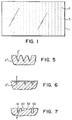
- a planar surface 3 of a light transmissive material 1 may contain a plurality of bores 2 therein.
- the bores 2 form regions which function to vary the effective refractive index of the light transmissive material 1.
- the refractive index of the light transmissive material may be varied by altering the number of bores (i.e., regions) within the particular area.
- the planar surface 3 may be divided into half sides. The left half side containing a lower density, or less number of bores per unit area, than the right half side containing a higher density or higher number of bores per unit area. The higher the density of holes, the higher the reduction of the refractive index in that area of the planar surface.
- the right half side of the planar surface in FIG. 1 will have a higher refractive index than the left half side.
- An average refractive index over a particular area of the planar surface may be achieved by selectively varying the density or number of holes in a planar surface of a light transmissive material.
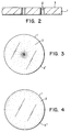
- FIG. 2 depicts a bore 2 in the form of a hole extending through the planar surface and completely through a light transmissive material 1.
- all bores need not extend through the planar surface. Variations in the depths of the bore, will produce a variation in the index of refraction of the planar surface. Generally, the deeper the bore, the higher the change in the index of refraction of the light transmissive material.
- the lateral dimensions of the bores should be smaller than the wave length of light which will pass through the planar surface of the light transmissive material. Preferably, the effective diameter of the lateral dimension should be less than approximately one-tenth to one-thirtieth the wavelength of light to be transmitted through the planar surface.
- FIG. 3 a disc shaped planar surface 3' made of a light transmissive material 1 having a plurality of bores 2 therein is shown.
- the density of the bores is greater in the center of the planar surface than at the outer edge thereof.
- the density of the holes 2 may vary uniformly along the radius of the disc shaped planar surface 3'.
- the holes along any imaginary circle or disc located at any particular radial dimension from the center are evenly spaced.
- the density of the bores 2, the number of bores per unit area, progressively increases along each imaginary ring within the disc shaped surface 3' towards the center of the surface 3'.
- the density of the bores 2 may vary according to the suggested formula or similar relationship to achieve the equivalent of a conventional lens with a spherical planar surface 3'.
- FIG. 4 depicts another disc shaped planar surface 3'' of a light transmissive material.
- the bores 2 therein are oriented such that the planar surface acts as the equivalent of a convex lens when light is transmitted therethrough.
- the density of the holes is greater towards the edge of the disc shaped planar surface.
- the spacing of the bores along any imaginary ring at a given distance from the center of the planar surface should be equal so that the index of refraction is the same throughout such an imaginary ring.
- Variations in the effective refractive index of a planar surface of a light transmissive material may be achieved not only by varying the density of bores within the planar surface, but varying the depth of the bores, and/or the width of the bores.
- a combination of varying density of bores and varying depths of bores may be used together to create a variation of the effective refractive index of the planar surface of a light transmissive material.
- an area of a planar surface with high reflectivity may be modified to reduce the reflectance of certain surface areas by creating bores in certain patterns which result in a low effective index of refraction at the planar surface and a progressively higher index of refraction in areas of increasing depth.
- a reduced reflective area may be formed by creating tapered bores 2' wherein the diameter of the bore decreases linearally with depth of the bore through the planar surface.
- a plurality of similar tapered bores 2' may be used to create an area of reduced reflectance.
- FIG. 6 depicts an area of a planar surface of light transmissive material having a plurality of bores 2 therein of varying depths but of relatively equal diameter. Each bore 2 is created so that its depth is slightly larger than the depth of a closest bore. Along any given line in the planar surface 3''' the depth of bores progressively increases to a desired depth and then progressively decreases to a desired depth eventually progressively increasing again to a desired depth.
- varying the refractive index can also be achieved by varying the width of the bores 12, 22, 32, 42 as well as the density and depth of the bores. Also, variations in effective refractive index may be achieved by filling some or all of the bores with a transparent material 9 such as aluminum having a refractive index greater, or less than, the refractive index of the planar surface of light transmissive material or the average refractive index of the light transmissive material which has been altered with bores, 12, 22, 32, 42 therein. Also, to minimize unwanted diffraction of the light passing through the planar surface, bore positions may be randomly placed within a region of nominally uniform bore density on the planar surface (not shown).
- an infrared optical light transmitting element or device may be formed using a uniformly thin wafer of silicon as a planar surface of light transmissive material.
- the silicon should be a single crystal wafer such as the type which is commonly prepared for semiconductor processing.
- the silicon wafer may be doped to produce an initial refractive index for the planar surface. If desired, the silicon wafer may be made thinner in the specific areas which will be used as the planar surface for light transmission therethrough. Bores may then be made in the planar surface. The exact pattern will depend upon the desired variation of refractive index.
- the bores may be created in the silicon surface by various lithographic processes, for example, reactive ion etching processes commonly used in semiconductor processing.
- these lithographic processes may be used to produce light transmitting devices in accordance with the principles of the present invention which are designed for transmitting the visible portions of the light spectrum.
- Commonly used lithographic processes are sufficient to create bores which are small enough compared to the wavelength of visible light.
- electron beam lithography, ion beam lithography or X-ray lithography may be used to create sufficiently small bores and reactive ion etching may be used to etch the same size bores.
- Specific high-resolution lithographic processes such as electron-beam lithography, X-ray lithography, ion-beam lithography or holographic lithography may also be used.
- These light transmitting devices may be fabricated in a manner that many devices are formed simultaneously similar to the fabrication of semiconductor wafers.
- Materials other than silicon may be used to create the planar surface of light transmissive material.
- conventional optical glasses germanium, silicon oxides, germanium oxides, ZnS, ZnSe, CaF2, BaF2, Al2O3, and polymers such as polymethyl methacrylate, as well as other light transmitting materials well known in the art may be used.
- Other crystalline semiconductors such as germanium, their oxides such as SiO2, glasses such as borosilicates, plastics such as polymethyl methacrylate (“Plexiglas”) and other materials otherwise suitable for optical elements may also be used.
- the aforementioned lithographic processes including reactive ion etching may be used to alter and/or improve the performance of optical elements which have already been performed by conventional grinding and polishing.
- Alteration of the refractive index may be achieved by creating a pattern of small bores in one surface on a conventional lens, such as an infrared lens having a spherical aberration to be corrected.
- the bore pattern to be created must be calculated to produce a variation of the effect of refractive index corresponding to a correction plate made by conventional means.
- the light transmitting device constructed in accordance with the principles of the present invention may be easily integrated with sensors as compared to conventional optical elements. For example, infrared sensor integration whereby the sensors are formed on one side of the silicon wafer light transmitting substrate may be easily accomplished. Alternatively, a light transmitting device may be easily bonded to a separate silicon detector by anodic bonding. Also, grooves may be created by etching, or other well known techniques, in either the light transmitting device or a silicon sensor while cementing fiber optic elements into the grooves.
- a prism made by the method described can be made contiguous to a photodiode junction near the surface of a semiconductor, and thereby direct light that is more or less normally incident on the wafer surface toward the photodiode junction.
- light emitted from the junction region of a light-emitting diode (LED) can be redirected by integrated optical elements of the present invention.
Landscapes
- Physics & Mathematics (AREA)
- General Physics & Mathematics (AREA)
- Optics & Photonics (AREA)
- Diffracting Gratings Or Hologram Optical Elements (AREA)
- Optical Couplings Of Light Guides (AREA)
Applications Claiming Priority (2)
| Application Number | Priority Date | Filing Date | Title |
|---|---|---|---|
| US160567 | 1993-12-01 | ||
| US08/160,567 US5585968A (en) | 1993-12-01 | 1993-12-01 | Optical elements having regions of different indices of refraction and method of fabricating the same |
Publications (2)
| Publication Number | Publication Date |
|---|---|
| EP0656549A2 true EP0656549A2 (de) | 1995-06-07 |
| EP0656549A3 EP0656549A3 (de) | 1996-01-17 |
Family
ID=22577421
Family Applications (1)
| Application Number | Title | Priority Date | Filing Date |
|---|---|---|---|
| EP94117742A Withdrawn EP0656549A3 (de) | 1993-12-01 | 1994-11-10 | Optische Elemente und Herstellungsverfahren. |
Country Status (3)
| Country | Link |
|---|---|
| US (2) | US5585968A (de) |
| EP (1) | EP0656549A3 (de) |
| JP (1) | JP2794084B2 (de) |
Families Citing this family (41)
| Publication number | Priority date | Publication date | Assignee | Title |
|---|---|---|---|---|
| US6893816B1 (en) * | 1993-10-28 | 2005-05-17 | Houston Advanced Research Center | Microfabricated, flowthrough porous apparatus for discrete detection of binding reactions |
| AU700315B2 (en) * | 1993-10-28 | 1998-12-24 | Houston Advanced Research Center | Microfabricated, flowthrough porous apparatus for discrete detection of binding reactions |
| US5813744A (en) * | 1997-03-17 | 1998-09-29 | Mcdonnell Douglas Corp. | Aircraft ground floodlight |
| US5840447A (en) * | 1997-08-29 | 1998-11-24 | International Business Machines Corporation | Multi-phase photo mask using sub-wavelength structures |
| US5978157A (en) * | 1998-09-03 | 1999-11-02 | Space Systems/ Loral, Inc. | Dielectric bootlace lens |
| US6619799B1 (en) | 1999-07-02 | 2003-09-16 | E-Vision, Llc | Optical lens system with electro-active lens having alterably different focal lengths |
| JP2002141556A (ja) * | 2000-09-12 | 2002-05-17 | Lumileds Lighting Us Llc | 改良された光抽出効果を有する発光ダイオード |
| US6963437B2 (en) * | 2000-10-03 | 2005-11-08 | Gentex Corporation | Devices incorporating electrochromic elements and optical sensors |
| US7293871B2 (en) * | 2000-11-27 | 2007-11-13 | Ophthonix, Inc. | Apparatus and method of correcting higher-order aberrations of the human eye |
| US6813082B2 (en) * | 2000-11-27 | 2004-11-02 | Ophthonix, Inc. | Wavefront aberrator and method of manufacturing |
| US7217375B2 (en) * | 2001-06-04 | 2007-05-15 | Ophthonix, Inc. | Apparatus and method of fabricating a compensating element for wavefront correction using spatially localized curing of resin mixtures |
| JP3743637B2 (ja) * | 2001-08-23 | 2006-02-08 | 独立行政法人理化学研究所 | フォトニック結晶および光導波素子 |
| US6682195B2 (en) | 2001-10-25 | 2004-01-27 | Ophthonix, Inc. | Custom eyeglass manufacturing method |
| US6712466B2 (en) | 2001-10-25 | 2004-03-30 | Ophthonix, Inc. | Eyeglass manufacturing method using variable index layer |
| US7434931B2 (en) | 2001-10-25 | 2008-10-14 | Ophthonix | Custom eyeglass manufacturing method |
| US7420743B2 (en) * | 2002-07-11 | 2008-09-02 | Ophthonix, Inc. | Optical elements and methods for making thereof |
| US6836371B2 (en) * | 2002-07-11 | 2004-12-28 | Ophthonix, Inc. | Optical elements and methods for making thereof |
| EP1424570A1 (de) * | 2002-11-28 | 2004-06-02 | Avanex Corporation | Fokussiereinrichtung |
| US7282306B2 (en) * | 2004-03-26 | 2007-10-16 | Intel Corporation | Continuous sloped phase edge architecture fabrication technique using electron or optical beam blur for single phase shift mask ret |
| US20050260388A1 (en) * | 2004-05-21 | 2005-11-24 | Lai Shui T | Apparatus and method of fabricating an ophthalmic lens for wavefront correction using spatially localized curing of photo-polymerization materials |
| FR2872590B1 (fr) * | 2004-07-02 | 2006-10-27 | Essilor Int | Procede de realisation d'un verre ophtalmique et composant optique adapte pour la mise en oeuvre de ce procede |
| FR2879757B1 (fr) * | 2004-12-17 | 2007-07-13 | Essilor Int | Procede de realisation d'un element optique transparent, composant optique intervenant dans ce procede et element optique ainsi obtenu |
| FR2888951B1 (fr) * | 2005-07-20 | 2008-02-08 | Essilor Int | Composant optique pixellise aleatoirement, son procede de fabrication, et son utilisation dans la fabrication d'un element optique transparent |
| FR2888947B1 (fr) * | 2005-07-20 | 2007-10-12 | Essilor Int | Composant optique a cellules |
| FR2888948B1 (fr) | 2005-07-20 | 2007-10-12 | Essilor Int | Composant optique transparent pixellise comprenant un revetement absorbant, son procede de realisation et son utilisation dans un element optique |
| FR2907559B1 (fr) * | 2006-10-19 | 2009-02-13 | Essilor Int | Composant optique elecro-commandable comprenant un ensemble de cellules |
| FR2910642B1 (fr) * | 2006-12-26 | 2009-03-06 | Essilor Int | Composant optique transparent a deux ensembles de cellules |
| EP1944808A1 (de) * | 2007-01-15 | 2008-07-16 | Stmicroelectronics Sa | Optisches Bildaufnehmermodul zur Verbindung mit einem optischen Halbleiterteil und Verfahren zu dessen Herstellung |
| FR2911404B1 (fr) * | 2007-01-17 | 2009-04-10 | Essilor Int | Composant optique transparent a cellules remplies de materiau optique |
| TW200913238A (en) * | 2007-06-04 | 2009-03-16 | Sony Corp | Optical member, solid state imaging apparatus, and manufacturing method |
| KR101204614B1 (ko) * | 2008-02-20 | 2012-11-23 | 도쿄엘렉트론가부시키가이샤 | 가스 공급 장치, 성막 장치, 및 성막 방법 |
| FR2930372B1 (fr) * | 2008-04-18 | 2011-05-27 | St Microelectronics Sa | Element et module optique imageur pour composant semi-conducteur optique, procede pour le traitement d'un element optique imageur et appareil de captation d'images |
| EP3973931A1 (de) * | 2008-12-22 | 2022-03-30 | Medical College of Wisconsin, Inc. | Verfahren und vorrichtung zur begrenzung des augenlängenwachstums |
| GB0916727D0 (en) * | 2009-09-23 | 2009-11-04 | Univ St Andrews | Improvements in or relating to imaging |
| US8752959B2 (en) * | 2010-07-13 | 2014-06-17 | Shamir Optical Industry Ltd. | Method and system for designing opthalmic lenses |
| US9354398B2 (en) | 2012-01-10 | 2016-05-31 | Hewlett Packard Enterprise Development Lp | Optical connectors |
| US10042091B2 (en) * | 2012-09-29 | 2018-08-07 | Purdue Research Foundation | Holey optical device |
| US10268050B2 (en) | 2015-11-06 | 2019-04-23 | Hoya Lens Thailand Ltd. | Spectacle lens |
| CA3032668A1 (en) * | 2016-08-01 | 2018-02-08 | University Of Washington | Ophthalmic lenses for treating myopia |
| EP3625620A4 (de) | 2017-05-08 | 2021-07-21 | SIGHTGLASS VISION, Inc. | Kontaktlinsen zur reduzierung von myopie und herstellungsverfahren dafür |
| US10884264B2 (en) | 2018-01-30 | 2021-01-05 | Sightglass Vision, Inc. | Ophthalmic lenses with light scattering for treating myopia |
Citations (4)
| Publication number | Priority date | Publication date | Assignee | Title |
|---|---|---|---|---|
| US3650598A (en) * | 1968-10-01 | 1972-03-21 | Nippon Selfoc Co Ltd | Light-conducting glass structure having a peripheral light-absorbent layer |
| FR2540638A1 (fr) * | 1983-02-04 | 1984-08-10 | Hoya Corp | Procede de production d'une lentille en forme de lame presentant un gradient de son indice de refraction dans la seule direction de son epaisseur |
| EP0349144A2 (de) * | 1988-06-29 | 1990-01-03 | Nec Corporation | Doppelbrechender Gitterpolarisator |
| EP0368751A1 (de) * | 1988-11-09 | 1990-05-16 | ESSILOR INTERNATIONAL Compagnie Générale d'Optique | Strukturierte Diffraktionskontaktlinse |
Family Cites Families (24)
| Publication number | Priority date | Publication date | Assignee | Title |
|---|---|---|---|---|
| DE3030936A1 (de) * | 1980-08-16 | 1982-04-01 | Clouth Gummiwerke AG, 5000 Köln | Einrichtung zum lagern von schienen fuer schienenfahrzeuge |
| FR2491632A1 (fr) * | 1980-10-08 | 1982-04-09 | Commissariat Energie Atomique | Lentille de fresnel integree et son procede de fabrication |
| US4462662A (en) * | 1981-06-15 | 1984-07-31 | Xerox Corporation | Imaging system utilizing a gradient index lens array compensated for non-uniform object illumination |
| JPS58166340A (ja) * | 1982-03-26 | 1983-10-01 | Olympus Optical Co Ltd | 画像形成装置 |
| US4528260A (en) * | 1983-04-27 | 1985-07-09 | Rca Corporation | Method of fabricating lenticular arrays |
| US4524127A (en) * | 1983-04-27 | 1985-06-18 | Rca Corporation | Method of fabricating a silicon lens array |
| US4737946A (en) * | 1984-09-03 | 1988-04-12 | Omron Tateisi Electronics Co. | Device for processing optical data with improved optical allignment means |
| JPS61106425A (ja) * | 1984-10-27 | 1986-05-24 | Canon Inc | 光学素子の製造方法 |
| GB2169595B (en) * | 1984-12-13 | 1989-06-07 | Canon Kk | Method of establishing a glass material in fine pores of porous glass. |
| JPS61188518A (ja) * | 1985-02-18 | 1986-08-22 | Canon Inc | ソフトフオ−カスフイルタ− |
| JPS61248001A (ja) * | 1985-04-26 | 1986-11-05 | Toshiba Corp | グレ−デイングレンズ |
| JPS6218502A (ja) * | 1985-07-18 | 1987-01-27 | Toshiba Corp | 光学装置 |
| JPS6370203A (ja) * | 1986-09-11 | 1988-03-30 | Brother Ind Ltd | 屈折率分布型光導波路レンズの製造方法 |
| US4878724A (en) * | 1987-07-30 | 1989-11-07 | Trw Inc. | Electrooptically tunable phase-locked laser array |
| JP2572626B2 (ja) * | 1988-04-28 | 1997-01-16 | 旭光学工業株式会社 | 焦点板及び微細構造配列体の形成方法 |
| US4912014A (en) * | 1988-10-17 | 1990-03-27 | The Mead Corporation | Imaging sheet having an open porous matrix containing a photohardenable composition, and a method for use of such a sheet |
| JPH02156204A (ja) * | 1988-12-08 | 1990-06-15 | Toyobo Co Ltd | マイクロカラーフィルターアレイとその製法 |
| US4948214A (en) * | 1989-07-10 | 1990-08-14 | Eastman Kodak Company | Step-index light guide and gradient index microlens device for LED imaging |
| US4936666A (en) * | 1989-08-08 | 1990-06-26 | Minnesota Mining And Manufacturing Company | Diffractive lens |
| JPH03165569A (ja) * | 1989-11-24 | 1991-07-17 | Nippon Sheet Glass Co Ltd | 画像伝送素子及びその製造方法 |
| GB2255483A (en) * | 1990-05-02 | 1992-11-04 | Darrell Dicicco | Beam-diverging multi-aperture diffraction plate |
| US5062688A (en) * | 1990-09-14 | 1991-11-05 | Nippon Sheet Glass Co., Ltd. | Flat plate optical element and method for preparing the same |
| US5164945A (en) * | 1991-07-01 | 1992-11-17 | Laser Centers Of America, Inc. | Laser device with intermediate refraction index layer for reduced fresnel losses |
| US5253103A (en) * | 1992-01-29 | 1993-10-12 | The University Of Rochester | Nonlinear optics utilizing composite optical material architectures for providing enhanced nonlinear susceptibility |
-
1993
- 1993-12-01 US US08/160,567 patent/US5585968A/en not_active Expired - Fee Related
-
1994
- 1994-11-10 EP EP94117742A patent/EP0656549A3/de not_active Withdrawn
- 1994-11-16 JP JP6281720A patent/JP2794084B2/ja not_active Expired - Lifetime
-
1997
- 1997-06-17 US US08/877,424 patent/US5808806A/en not_active Expired - Fee Related
Patent Citations (4)
| Publication number | Priority date | Publication date | Assignee | Title |
|---|---|---|---|---|
| US3650598A (en) * | 1968-10-01 | 1972-03-21 | Nippon Selfoc Co Ltd | Light-conducting glass structure having a peripheral light-absorbent layer |
| FR2540638A1 (fr) * | 1983-02-04 | 1984-08-10 | Hoya Corp | Procede de production d'une lentille en forme de lame presentant un gradient de son indice de refraction dans la seule direction de son epaisseur |
| EP0349144A2 (de) * | 1988-06-29 | 1990-01-03 | Nec Corporation | Doppelbrechender Gitterpolarisator |
| EP0368751A1 (de) * | 1988-11-09 | 1990-05-16 | ESSILOR INTERNATIONAL Compagnie Générale d'Optique | Strukturierte Diffraktionskontaktlinse |
Also Published As
| Publication number | Publication date |
|---|---|
| JP2794084B2 (ja) | 1998-09-03 |
| EP0656549A3 (de) | 1996-01-17 |
| US5585968A (en) | 1996-12-17 |
| JPH07198907A (ja) | 1995-08-01 |
| US5808806A (en) | 1998-09-15 |
Similar Documents
| Publication | Publication Date | Title |
|---|---|---|
| US5585968A (en) | Optical elements having regions of different indices of refraction and method of fabricating the same | |
| EP0649037B1 (de) | Diffraktive optische Einrichtung | |
| US11719956B2 (en) | Ophthalmic lens with graded microlenses | |
| KR0172601B1 (ko) | 회절렌즈 | |
| US11222987B2 (en) | Optical receiver employing a metasurface collection lens having concentric belts or rings | |
| US5541774A (en) | Segmented axial gradient lens | |
| US4210391A (en) | Multifocal zone plate | |
| US5285314A (en) | Superzone holographic mirror | |
| US7263249B2 (en) | Optical element assembly and method of making the same | |
| CA2302528A1 (en) | Integrated beam shaper and use thereof | |
| KR19990029524A (ko) | 침지 시스템 | |
| US20040247010A1 (en) | Antireflection diffraction grating | |
| EP0050545A1 (de) | Integrierte Fresnelsche Linse und deren Herstellungsverfahren | |
| JP2001004827A (ja) | 段付エタロン | |
| US5258862A (en) | Rotating disc optical synchronization system using binary diffractive optical elements | |
| JP3189922B2 (ja) | 回折光学素子 | |
| US20050287445A1 (en) | Method of making grayscale mask for grayscale doe production by using an absorber layer | |
| EP0620201A2 (de) | Verfahren zur Herstellung von mikrooptischen Bauteilen | |
| US5448403A (en) | Binary diffractive optical element scanner | |
| JP3214964B2 (ja) | 回折光学素子 | |
| US5387961A (en) | Illumination system for projection exposing apparatus | |
| US20040240034A1 (en) | Diffraction compensation using a patterned reflector | |
| US5161058A (en) | Focusing screen | |
| JPH0644082B2 (ja) | 平板状レンズ | |
| JPH0749407A (ja) | 赤外用フレネルレンズ |
Legal Events
| Date | Code | Title | Description |
|---|---|---|---|
| PUAI | Public reference made under article 153(3) epc to a published international application that has entered the european phase |
Free format text: ORIGINAL CODE: 0009012 |
|
| AK | Designated contracting states |
Kind code of ref document: A2 Designated state(s): DE FR GB |
|
| PUAL | Search report despatched |
Free format text: ORIGINAL CODE: 0009013 |
|
| 17P | Request for examination filed |
Effective date: 19951024 |
|
| AK | Designated contracting states |
Kind code of ref document: A3 Designated state(s): DE FR GB |
|
| STAA | Information on the status of an ep patent application or granted ep patent |
Free format text: STATUS: THE APPLICATION HAS BEEN WITHDRAWN |
|
| 18W | Application withdrawn |
Withdrawal date: 19961125 |