EP0655647A1 - Color filter, method for manufacturing it, and liquid crystal panel - Google Patents
Color filter, method for manufacturing it, and liquid crystal panel Download PDFInfo
- Publication number
- EP0655647A1 EP0655647A1 EP94118432A EP94118432A EP0655647A1 EP 0655647 A1 EP0655647 A1 EP 0655647A1 EP 94118432 A EP94118432 A EP 94118432A EP 94118432 A EP94118432 A EP 94118432A EP 0655647 A1 EP0655647 A1 EP 0655647A1
- Authority
- EP
- European Patent Office
- Prior art keywords
- color filter
- portions
- resin layer
- substrate
- light irradiation
- Prior art date
- Legal status (The legal status is an assumption and is not a legal conclusion. Google has not performed a legal analysis and makes no representation as to the accuracy of the status listed.)
- Granted
Links
Images


Classifications
-
- B—PERFORMING OPERATIONS; TRANSPORTING
- B41—PRINTING; LINING MACHINES; TYPEWRITERS; STAMPS
- B41M—PRINTING, DUPLICATING, MARKING, OR COPYING PROCESSES; COLOUR PRINTING
- B41M5/00—Duplicating or marking methods; Sheet materials for use therein
- B41M5/50—Recording sheets characterised by the coating used to improve ink, dye or pigment receptivity, e.g. for ink-jet or thermal dye transfer recording
- B41M5/52—Macromolecular coatings
-
- B—PERFORMING OPERATIONS; TRANSPORTING
- B41—PRINTING; LINING MACHINES; TYPEWRITERS; STAMPS
- B41J—TYPEWRITERS; SELECTIVE PRINTING MECHANISMS, i.e. MECHANISMS PRINTING OTHERWISE THAN FROM A FORME; CORRECTION OF TYPOGRAPHICAL ERRORS
- B41J2/00—Typewriters or selective printing mechanisms characterised by the printing or marking process for which they are designed
- B41J2/005—Typewriters or selective printing mechanisms characterised by the printing or marking process for which they are designed characterised by bringing liquid or particles selectively into contact with a printing material
- B41J2/01—Ink jet
-
- B—PERFORMING OPERATIONS; TRANSPORTING
- B41—PRINTING; LINING MACHINES; TYPEWRITERS; STAMPS
- B41M—PRINTING, DUPLICATING, MARKING, OR COPYING PROCESSES; COLOUR PRINTING
- B41M3/00—Printing processes to produce particular kinds of printed work, e.g. patterns
- B41M3/003—Printing processes to produce particular kinds of printed work, e.g. patterns on optical devices, e.g. lens elements; for the production of optical devices
-
- B—PERFORMING OPERATIONS; TRANSPORTING
- B41—PRINTING; LINING MACHINES; TYPEWRITERS; STAMPS
- B41M—PRINTING, DUPLICATING, MARKING, OR COPYING PROCESSES; COLOUR PRINTING
- B41M7/00—After-treatment of prints, e.g. heating, irradiating, setting of the ink, protection of the printed stock
- B41M7/0045—After-treatment of prints, e.g. heating, irradiating, setting of the ink, protection of the printed stock using protective coatings or film forming compositions cured by mechanical wave energy, e.g. ultrasonics, cured by electromagnetic radiation or waves, e.g. ultraviolet radiation, electron beams, or cured by magnetic or electric fields, e.g. electric discharge, plasma
-
- B—PERFORMING OPERATIONS; TRANSPORTING
- B41—PRINTING; LINING MACHINES; TYPEWRITERS; STAMPS
- B41M—PRINTING, DUPLICATING, MARKING, OR COPYING PROCESSES; COLOUR PRINTING
- B41M7/00—After-treatment of prints, e.g. heating, irradiating, setting of the ink, protection of the printed stock
- B41M7/0054—After-treatment of prints, e.g. heating, irradiating, setting of the ink, protection of the printed stock using protective coatings or film forming compositions cured by thermal means, e.g. infrared radiation, heat
-
- G—PHYSICS
- G02—OPTICS
- G02B—OPTICAL ELEMENTS, SYSTEMS OR APPARATUS
- G02B5/00—Optical elements other than lenses
- G02B5/20—Filters
- G02B5/201—Filters in the form of arrays
-
- G—PHYSICS
- G03—PHOTOGRAPHY; CINEMATOGRAPHY; ANALOGOUS TECHNIQUES USING WAVES OTHER THAN OPTICAL WAVES; ELECTROGRAPHY; HOLOGRAPHY
- G03F—PHOTOMECHANICAL PRODUCTION OF TEXTURED OR PATTERNED SURFACES, e.g. FOR PRINTING, FOR PROCESSING OF SEMICONDUCTOR DEVICES; MATERIALS THEREFOR; ORIGINALS THEREFOR; APPARATUS SPECIALLY ADAPTED THEREFOR
- G03F7/00—Photomechanical, e.g. photolithographic, production of textured or patterned surfaces, e.g. printing surfaces; Materials therefor, e.g. comprising photoresists; Apparatus specially adapted therefor
- G03F7/0005—Production of optical devices or components in so far as characterised by the lithographic processes or materials used therefor
- G03F7/0007—Filters, e.g. additive colour filters; Components for display devices
-
- G—PHYSICS
- G03—PHOTOGRAPHY; CINEMATOGRAPHY; ANALOGOUS TECHNIQUES USING WAVES OTHER THAN OPTICAL WAVES; ELECTROGRAPHY; HOLOGRAPHY
- G03F—PHOTOMECHANICAL PRODUCTION OF TEXTURED OR PATTERNED SURFACES, e.g. FOR PRINTING, FOR PROCESSING OF SEMICONDUCTOR DEVICES; MATERIALS THEREFOR; ORIGINALS THEREFOR; APPARATUS SPECIALLY ADAPTED THEREFOR
- G03F7/00—Photomechanical, e.g. photolithographic, production of textured or patterned surfaces, e.g. printing surfaces; Materials therefor, e.g. comprising photoresists; Apparatus specially adapted therefor
- G03F7/004—Photosensitive materials
- G03F7/0045—Photosensitive materials with organic non-macromolecular light-sensitive compounds not otherwise provided for, e.g. dissolution inhibitors
-
- G—PHYSICS
- G03—PHOTOGRAPHY; CINEMATOGRAPHY; ANALOGOUS TECHNIQUES USING WAVES OTHER THAN OPTICAL WAVES; ELECTROGRAPHY; HOLOGRAPHY
- G03F—PHOTOMECHANICAL PRODUCTION OF TEXTURED OR PATTERNED SURFACES, e.g. FOR PRINTING, FOR PROCESSING OF SEMICONDUCTOR DEVICES; MATERIALS THEREFOR; ORIGINALS THEREFOR; APPARATUS SPECIALLY ADAPTED THEREFOR
- G03F7/00—Photomechanical, e.g. photolithographic, production of textured or patterned surfaces, e.g. printing surfaces; Materials therefor, e.g. comprising photoresists; Apparatus specially adapted therefor
- G03F7/004—Photosensitive materials
- G03F7/038—Macromolecular compounds which are rendered insoluble or differentially wettable
- G03F7/0382—Macromolecular compounds which are rendered insoluble or differentially wettable the macromolecular compound being present in a chemically amplified negative photoresist composition
-
- G—PHYSICS
- G03—PHOTOGRAPHY; CINEMATOGRAPHY; ANALOGOUS TECHNIQUES USING WAVES OTHER THAN OPTICAL WAVES; ELECTROGRAPHY; HOLOGRAPHY
- G03F—PHOTOMECHANICAL PRODUCTION OF TEXTURED OR PATTERNED SURFACES, e.g. FOR PRINTING, FOR PROCESSING OF SEMICONDUCTOR DEVICES; MATERIALS THEREFOR; ORIGINALS THEREFOR; APPARATUS SPECIALLY ADAPTED THEREFOR
- G03F7/00—Photomechanical, e.g. photolithographic, production of textured or patterned surfaces, e.g. printing surfaces; Materials therefor, e.g. comprising photoresists; Apparatus specially adapted therefor
- G03F7/004—Photosensitive materials
- G03F7/039—Macromolecular compounds which are photodegradable, e.g. positive electron resists
-
- B—PERFORMING OPERATIONS; TRANSPORTING
- B41—PRINTING; LINING MACHINES; TYPEWRITERS; STAMPS
- B41J—TYPEWRITERS; SELECTIVE PRINTING MECHANISMS, i.e. MECHANISMS PRINTING OTHERWISE THAN FROM A FORME; CORRECTION OF TYPOGRAPHICAL ERRORS
- B41J2202/00—Embodiments of or processes related to ink-jet or thermal heads
- B41J2202/01—Embodiments of or processes related to ink-jet heads
- B41J2202/09—Ink jet technology used for manufacturing optical filters
-
- B—PERFORMING OPERATIONS; TRANSPORTING
- B41—PRINTING; LINING MACHINES; TYPEWRITERS; STAMPS
- B41M—PRINTING, DUPLICATING, MARKING, OR COPYING PROCESSES; COLOUR PRINTING
- B41M5/00—Duplicating or marking methods; Sheet materials for use therein
- B41M5/50—Recording sheets characterised by the coating used to improve ink, dye or pigment receptivity, e.g. for ink-jet or thermal dye transfer recording
- B41M5/52—Macromolecular coatings
- B41M5/5227—Macromolecular coatings characterised by organic non-macromolecular additives, e.g. UV-absorbers, plasticisers, surfactants
-
- B—PERFORMING OPERATIONS; TRANSPORTING
- B41—PRINTING; LINING MACHINES; TYPEWRITERS; STAMPS
- B41M—PRINTING, DUPLICATING, MARKING, OR COPYING PROCESSES; COLOUR PRINTING
- B41M5/00—Duplicating or marking methods; Sheet materials for use therein
- B41M5/50—Recording sheets characterised by the coating used to improve ink, dye or pigment receptivity, e.g. for ink-jet or thermal dye transfer recording
- B41M5/52—Macromolecular coatings
- B41M5/5254—Macromolecular coatings characterised by the use of polymers obtained by reactions only involving carbon-to-carbon unsaturated bonds, e.g. vinyl polymers
Definitions
- the present invention relates to a color filter suitable for a color liquid crystal display which can be used in a color television, a personal computer or the like, a method for manufacturing the color filter, and a liquid crystal panel equipped with the color filter. More specifically, it relates to a color filter for liquid crystal displays manufactured by the utilization of an ink jet recording technique, a method for manufacturing the color filter, and a liquid crystal panel equipped with the color filter.
- a first method which has most often been used is a dyeing method.
- This dyeing method comprises coating a glass substrate with an aqueous polymer material which is a material to be dyed, patterning the material into a desired shape by a photolithography process, and then immersing the thus obtained pattern in a dyeing bath to obtain a colored pattern. This operation is repeated three times to form the colored layers of Red (R), Green (G) and Blue (B).
- Japanese Patent Application Laid-Open No. 5-288913 has described another example of this dyeing method which comprises forming a photosensitive layer, exposing it to light through a pattern, dyeing unexposed portions, and then repeating this process to manufacture a color filter having three colors of R, G and B.
- a second method is a pigment dispersion method, which is now being replaced with the above-mentioned dyeing method.
- This pigment dispersion method comprises first forming, on a substrate, a photosensitive resin layer in which a pigment is dispersed, and then patterning the resin layer to obtain a single-colored pattern. Next, this process is repeated three times to form colored layers having three colors of R, G and B.
- a third method is an electrodeposition method. This method comprises first patterning transparent electrodes on a substrate, and then immersing it in an electrodeposition coating solution containing a pigment, a resin, an electrolyte and the like to electrodeposit a first color. This process is repeated three times to form colored layers of R, G and B, and in the last step, these layers are calcined.
- a fourth method is a printing method. This method comprises dispersing a pigment in a thermosetting resin, repeating a printing operation three times to coat with the colors of R, G and B, and then thermosetting the colored resin layers to form colored layers. In each of these methods, a protective layer is usually formed on the colored layers.
- a point which is common to these methods is that a similar process is required to be repeated three times to give the three colors of R, G and B, which increases the cost.
- these methods having many steps lead to deterioration of a yield.
- the formable patterns are limited, and so it is difficult to apply this method to TFT by an existent technique.
- the printing method has a drawback that resolution properties and smoothing properties are poor, and so it is not suitable for the formation of a pattern having a fine pitch.
- an object of the present invention is to provide a method for manufacturing a color filter at a law cost in which necessary characteristics such as heat resistance, solvent resistance and resolution properties given by a conventional method are kept up, an ink jet suitability is satisfied, and a process for its manufacture is shortened; a highly reliable color filter manufactured by the above-mentioned method; and a liquid crystal panel equipped with the above-mentioned color filter.
- an object of the present invention is to provide a highly precise and reliable color filter for liquid crystals which can prevent color mixing and color skip when ink droplets are ejected by the use of an ink jet system to carry out the arrangement of colorants; and a method for manufacturing the color filter.
- a first aspect of the present invention is directed to a color filter which comprises a substrate and a resin layer on the substrate, the resin layer containing a plurality of colored portions of different colors and non-colored portions.
- a second aspect of the present invention is directed to a color filter which comprises a substrate having shade portions and light-transmittable portions and a resin layer on the substrate, the resin layer on the shade portions containing colored portions and non-colored portions.
- a third aspect of the present invention is directed to a method for manufacturing a color filter which comprises arranging colorants on a substrate by an ink jet system, said method being characterized by comprising:
- a fourth aspect of the present invention is directed to a liquid crystal panel which comprises a color filter described above, a substrate facing to the color filter, and a liquid crystal compound enclosed between both the substrates.
- a fifth aspect of the present invention is directed to a liquid crystal panel which comprises a color filter described above, a substrate having shape portions arranged at a position opposite to the color filter, and a liquid crystal composition enclosed between the color filter and the substrate.
- a sixth aspect of the present invention is directed to a method for manufacturing a color filter which comprises arranging colorants on a substrate by an ink jet system, said method being characterized by comprising:
- a seventh aspect of the present invention is directed to a color filter which comprises a substrate having light-transmittable portions and a resin layer having the colored light-transmittable portions on the substrate, said resin layer being characterized by comprising at least (a) a homopolymer of a monomer comprising a structure unit represented by the following formula (I) and/or a copolymer of the above-mentioned monomer and another vinyl monomer, and (b) a compound selected from the group consisting of halogenated triazine compounds, diphenyliodonium salt derivatives and triphenylsulfonium salt derivatives: wherein R1 is hydrogen or a methyl group; and R2 is a hydrogen atom or an alkyl group having 1 to 5 carbon atoms.
- An eighth aspect of the present invention is directed to a method for manufacturing a color filter which comprises arranging colorants on a substrate having shade portions by an ink jet system, said method comprising:
- a ninth aspect of the present invention is directed to a liquid crystal panel which comprises a color filter described in eighth aspect, a substrate arranged at a position opposite to the color filter, and a liquid crystal composition enclosed between the color filter and the substrate.
- a tenth aspect of the present invention is directed to a method for manufacturing a color filter which comprises arranging colorants on a substrate having light-transmittable portions by an ink jet system, said method being characterized by comprising:
- An eleventh aspect of the present invention is directed to a color filter manufactured by the method described in tenth aspect.
- a twelfth aspect of the present invention is directed to a color filter which comprises a substrate and a resin layer having colored light-transmittable portions on the substrate, said resin layer being characterized by comprising at least (a) an acrylic resin having a structure unit represented by the following formula (V) and (b) a compound selected from the group consisting of halogenated triazine compounds, diphenyliodonium salt derivatives and triphenylsulfonium salt derivatives: wherein R1 is hydrogen or an alkyl group having 1 to 5 carbon atoms; R2 is an alkylene group having 1 to 5 carbon atoms or a phenylene group; R3 is an alkyl group having 1 to 5 carbon atoms, an alkyl-substituted silyl group, a phenyl group or a substituted aromatic group.
- V an acrylic resin having a structure unit represented by the following formula (V)
- a thirteenth aspect of the present invention is directed to a method for manufacturing a color filter which comprises arranging colorants on a substrate by an ink jet system, said method comprising:
- a fourteenth aspect of the present invention is directed to a color filter manufactured by a manufacturing method described in thirteenth aspect.
- a fifteenth aspect of the present invention is directed to a liquid crystal panel which comprises a color filter described in twelfth aspect, a substrate arranged at a position facing to the color filter, and a liquid crystal composition sealed between the color filter and the substrate.
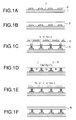
- Figs. 1A to 1E show a flow sheet of a manufacturing process of a color filter in the present invention, and in this drawing, one example of the constitution of the color filter of the present invention is shown.
- a substrate a light-transmittable substrate is preferable, and a glass substrate is usually used.
- the glass substrate is not restrictive, and any material can be used as the substrate, so long as it has necessary characteristics such as transparency and mechanical strength which the color filter for liquid crystals should have.
- Fig. 1A shows a glass substrate 1 having light-transmittable portions 7 and black matrices 2 which are shade portions.
- the substrate 1 provided with the black matrices 2 is coated with a resin composition which can cure by light irradiation or the light irradiation and heating to reduce an ink-acceptable property of the layer, and if necessary, prebaking is then carried out to form a resin layer 3 (Fig. 1B).
- a resin layer 3 Fig. 1B
- spin coating, roll coating, bar coating, spray coating or dip coating can be used, and this coating means is not particularly restrictive.
- portions of the resin layer which are shaded by the black matrices 2 are first pattern-exposed through a photomask 4 to cure these portions of the resin layers, thereby forming sites 8 (non-colored portions) which do not absorb an ink (Fig. 1C). Thereafter, the same layer is colored in colors of R, G and B by the use of an ink jet head 5 (Fig. 1D), and if necessary, the ink is then dried.
- the photomask 4 which can be used at the time of the pattern exposure has holes which permit the portions of the resin layer shaded by the black matrices to cure.
- a relatively large amount of the ink is required to be ejected from ink jet head.
- a dyestuff-type and a pigment-type ink are both usable, and both liquid inks and solid inks are also usable.
- the curable resin composition which can be used in the present invention, any one is acceptable, so long as it has an ink-receptable property and can cure by at least one treatment of light irradiation or the combination of the light irradiation and heating.
- the resin include acrylic resins, epoxy resins, silicon resins, cellulose derivatives such as hydroxypropyl cellulose, hydroxyethyl cellulose, methyl cellulose and carboxymethyl cellulose, and modified resins thereof.
- a photoinitiator (a crosslinking agent) can be used.
- the usable photoinitiator include dichromates, bisazido compounds, radical initiators, cationic initiators and anionic initiators. These photoinitiators can be used in combination, or they can be used with another sensitizer, when used.
- a heat treatment may be carried out after the light irradiation.
- the resin layer containing these components is very excellent in fastnesses to heat, water and the like, and it can sufficiently withstand a high temperature and washing in subsequent steps.
- an ink jet system which can be used in the present invention, there can be used a bubble jet type using an electricity-heat converter as an energy-generating element and a piezo jet type using a piezo-electric element.
- a colored area and a colored pattern can be optionally set.
- the black matrices are formed on the substrate, but they can be formed on the resin layer after the formation of the curable resin composition layer or the coloring without any particular problem. Therefore, the constitution of the black matrices in this embodiment is not restrictive.
- the black matrices can be preferably prepared by forming a metallic thin film on the substrate by sputtering or vapor deposition, and then patterning the film by photolithography, or alternatively patterning a photosensitive black resin. These procedures are not restrictive.
- the protective layer 6 is made of a second resin composition of a photosetting type, a thermosetting type or a photo-thermosetting type, or an inorganic material with the aid of vapor deposition or sputtering.
- any material can be used, so long as it does not impede the transparency of the obtained color filter, and can sufficiently withstand subsequent steps such as an ITO formation step and an orientation film formation step.
- Figs. 2A to 2E show a manufacturing process of the color filter for use in a liquid crystal panel in which the black matrices are provided on the opposite substrate.
- the method in which the black matrices are provided on the opposite substrate instead of the side of the color filter is effective as a technique of improving an aperture ratio.
- a glass substrate 1 shown in Fig. 2A is coated with a composition in which the ink absorbency of light irradiation portions deteriorates by the light irradiation or the combination of the light irradiation and the heat treatment, and if necessary, prebaking is then done to form a composition layer 3 in which the ink absorbency of the light irradiation portions deteriorates by the light irradiation or the combination of the light irradiation and the heat treatment (Fig. 2B).
- pattern exposure is carried out through a photomask 4 to reduce the ink absorbency of the exposed portions of the composition layer 3 (Fig. 2C), and then non-exposed portions of the same layer are colored in the colors of R, G and B by the use of an ink jet head 5 (Fig. 2D), followed by drying, if necessary.
- an ink jet head 5 Fig. 2D
- the colored resin composition layer is cured by the light irradiation and/or the heat treatment (Fig. 2E), and if necessary, a protective layer 6 is formed (Fig. 2F) to obtain a color filter.
- a protective layer there can be used a resin composition of a photosetting type, a thermosetting type or a photo-thermosetting type, or an inorganic material formed by vapor deposition or sputtering.
- any material can be used, so long as it does not impede the transparency of the obtained color filter, and can sufficiently withstand subsequent steps such as an ITO formation step and an oriented film formation step.
- the color filter is manufactured which has the resin layer, the plurality of colored portions having the different colors, and the non-colored portions on the substrate.
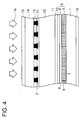
- Figs. 3 and 4 show sectional views of TFT color liquid crystal panels incorporated with the color filter of the present invention. These embodiments are not restrictive.
- the color liquid crystal panel can usually be formed by combining a color filter substrate 1 with a glass substrate 14, and then enclosing a liquid crystal compound 12 therebetween.
- TFT (not shown) and transparent pixel electrodes 13 are formed in the state of matrices.
- a color filter 9 is arranged so that the color materials of R, G and B are placed at a position opposite to the pixel electrodes, and all over the color filter 9, a transparent common electrode 10 is formed.
- Black matrices are formed on the side of the color filter substrate (Fig. 3), but in the case of a BM on-array type liquid crystal panel, they are formed on the faced TFT substrate side (Fig. 4).
- orientation films 11 are formed and then subjected to a rubbing treatment to arrange liquid crystal molecules in a certain direction. Furthermore, polarizing plates 15 adhere to the outsides of the respective glass substrates 1 and 14, and the liquid crystal compound 12 is filled into the space (about 2 to 5 ⁇ m) between these glass substrates.
- a back light 16 a combination of fluorescent lamps (not shown) and a scattering plate (not shown) is usually used, and display is carried out by utilizing the liquid crystal compound as a light shutter for changing the transmittance of the back light.
- Reference numeral 2 is a black matrix
- 3 is an ink receiving layer
- 6 is a protective layer
- 7 is a colored portions
- 8 is non-colored portions.
- a substrate on which black matrices are formed is coated with a resin composition layer which has ink-acceptable property and in which the residue of a hydrophilic group in light irradiation portions decreases by light irradiation or the combination of the light irradiation and heating, thereby forming the resin composition layer which has the ink-acceptable properties and in which the residue of the hydrophilic group in the light irradiation portions decreases by the light irradiation or the combination of the light irradiation and the heating.
- This method intends to prevent the mixing of the inks and the excessive diffusion of the ink by the utilization of a difference of ink absorbency between exposed portions and unexposed portions.
- the resin composition in which the ink absorbency of the light irradiation portions deteriorate by the light irradiation or the combination of the light irradiation and the heating, and in other words, it is preferable to use the resin composition which can give rise to crosslinking via a hydrophilic group such as an hydroxyl group, an alkoxy group or an amino group, or which brings about an additional reaction with the hydrophilic group.
- the absorbency deteriorate only by the light irradiation, but the heat treatment may be used together with the light irradiation to accelerate a crosslinking reaction without any problem.
- the resin composition which can be used in the present invention, a system utilizing the crosslinking reaction by chemical amplification is preferable.
- the basic resin include cellulose derivatives such as hydroxypropyl cellulose and hydroxyethyl cellulose, a high-molecular alcohol such as polyvinyl alcohol and its derivatives, a novolak resin such as cresol-novolak and its derivatives, and an acrylic resin containing an acrylic monomer having a hydroxyl group such as hydroxyethyl methacrylate.
- crosslinking agent includes a melamine derivative such as methylol melamine
- examples of the photoinitiator include an onium salt such as triphenylsulfonium hexafluoroantimonate and a halogenated organic compound such as trichloromethyltriazine. These examples are not restrictive.
- the particularly preferable resin composition which can be used in the present invention comprises at least (a) a homopolymer of a monomer comprising a structure unit represented by the following formula (I) and/or a copolymer of the above-mentioned monomer and another vinyl monomer, and (b) a compound selected from the group consisting of halogenated triazine compounds, diphenyliodonium salt derivatives and triphenylsulfonium salt derivatives: wherein R1 is hydrogen or a methyl group; and R2 is a hydrogen atom or an alkyl group having 1 to 5 carbon atoms.
- Examples of the monomer comprising the structure unit represented by the above formula (I) which is the component (a) include N-methylolacrylamide, N-methoxymethylacrylamide, N-ethoxymethylacrylamide, N-isopropoxymethylacrylamide, N-methylolmethacrylamide, N-methoxymethylmethacrylamide and N-ethoxymethylacrylamide, but they are not restrictive. Each of these monomers is used singly or may be copolymerized with another vinyl monomer.
- Examples of the other vinyl monomer include acrylic acid, methacrylic acid; acrylic acid esters such as methyl acrylate and ethyl acrylate; methacylic acid esters such as methyl methacrylate and ethyl methacrylate; vinyl monomers having a hydroxyl group such as hydroxymethyl methacrylate, hydroxyethyl methacrylate, hydroxymethyl acrylate and hydroxyethyl acrylate; styrene, ⁇ -methylstyrene, acrylamide, methacrylamide, acrylonitrile, allylamine, vinylamine, vinyl acetate and vinyl propionate. Needless to say, they are not restrictive.
- halogenated triazine compounds include compounds represented by the formula (II) wherein Z is a halogen atom; Y is CZ3 (Z is a halogen atom), phenyl, a halogenated phenyl, wherein R7 is an alkyl group having 1 to 5 carbon atoms, and when one group has two R7s, they may be different from each other.
- halogenated triazine compounds function as a photoinitiator, and they are preferably compounds in which a trichloromethyl group is introduced into a triazine ring, as in the compounds represented by the above-mentioned formula (II).
- halogenated triazine compounds include 2-(p-methoxyphenyl)-4,6-bis(trichloromethyl)-s-triazine, 2-styryl-4,6-bis(trichloromethyl)-s-triazine, 2-(p-methylstyryl)-4,6-bis(trichloromethyl)-s-triazine and 2-phenyl-4,6-bis(trichloromethyl)-s-triazine.
- the diphenyliodonium salt derivatives include compounds represented by the formula (III) wherein R4 and R5 are each hydrogen, an alkoxy group having 1 to 5 carbon atoms or t-butyl group; and X ⁇ is BF4 ⁇ , PF6 ⁇ , SbF6 ⁇ or CF3SO3 ⁇ .
- diphenyliodonium salt derivatives function as a photoinitiator, and typical examples thereof include diphenyliodonium hexafluoroantimonate, diphenyliodonium tetrafluoroborate, diphenyliodonium hexafluorophosphate, diphenyliodonium triflate and their derivatives. Needless to say, they are not restrictive.
- triphenylsulfonium salt derivatives include compounds represented by the formula (IV) wherein R6 is hydrogen, an alkyl group or an alkoxy group each having 1 to 5 carbon atoms, or fluorine; and X ⁇ is as defined above.
- triphenylsulfonium salt derivatives function as a photoinitiator, and typical examples thereof include triphenylsulfonium hexafluoroantimonate, triphenylsulfonium tetrafluoroborate, triphenylsulfonium hexafluorophosate, triphenylsulfonium triflate and their derivatives. Needless to say, they are not restrictive.
- the amount of the compound (b) is in the range of from 0.01 to 10 parts by weight, preferably from 0.01 to 5 parts by weight with respect to 100 parts by weight of the polymer which is the compound (a).
- the molecular weight of the above-mentioned polymer is preferably in the range of from 102 to 107.
- the employment of this kind of resin causes a definite difference of ink absorbency between an irradiated portion and a non-irradiated portion to permit the prevention of the color mixing of inks.
- a coating material of portions shaded with the black matrices is first subjected to pattern exposure (Fig. 1C), and the coloring of R, G and B is then made by the use of an ink jet head 5 (Fig. 1C). Afterward, if necessary, inks are dried.
- the residue of a hydrophilic group such as an hydroxyl group, an alkoxy group or an amino group decreases with the progress of the reaction, so that the exposed portions scarcely absorb the ink, whereby the mixture of the inks having the colors can be prevented.
- the residue of the hydrophilic group in the exposed portions is preferably decreased to 70% or less of the amount of the hydrophilic group in the unexposed portions.
- the photomask which can be used at the time of the pattern exposure has openings for exposing the portions shaded by the black matrices.
- the mask provided with the openings having a diameter smaller than the width of the portions shaded by the black matrices.
- a protective layer is then formed (Fig. 1F).
- the protective layer there can be used a resin material of a photosetting type, a thermosetting type or a photo-thermosetting type, or an inorganic film formed by vapor deposition or sputtering.
- any material can be used, so long as it does not impede the transparency of the obtained color filter, and can sufficiently withstand subsequent steps such as an ITO formation step and an oriented film formation step.
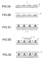
- Fig. 5A shows a glass substrate having black matrices thereon which are shade portions 2.
- the substrate provided with the black matrices is coated with a composition, in which the ink absorbency of light irradiated portions can be improved by light irradiation or the combination of the light irradiation and a heat treatment, and if necessary, prebaking is then carried out to form a resin layer 3 (Fig. 5B).
- this composition layer a coating method such as spin coating, roll coating, bar coating, spray coating or dip coating can be used, and this coating means is not particularly restrictive.
- a compound such as perylene, anthracene or phenothiazine may be added as a sensitizing agent to the composition layer.
- the composition layer is pattern-exposed through the black matrices as a mask to improve the ink absorbency of the irradiated portions of the composition layer (Fig. 5C).
- openings which are the irradiated portions are colored with colors of R, G and B by the use of an ink jet head 5 (Fig. 5D), and if necessary, the inks are then dried.
- the portions of the composition layer having a larger area than the openings of the black matrices are preferably colored, and for this coloring, it is necessary that the portions of the composition layer having a larger area than the black matrices as the mask take part in reaction.
- some means are effective, and for example, diffused light can be used as irradiation light at the time of exposure, a large excess of energy can be irradiated, or a heat treatment is carried out for a long period of time after the exposure to diffuse the reaction.
- the pattern exposure is carried out by the use of the black matrices as the mask, but the pattern exposure may be done from the upside of the resin composition layer by the use of another photomask.
- Figs. 6A to 6E show a method for preparing a color filter for use in a liquid crystal panel in which the black matrices are formed on an opposite substrate.
- the method in which the black matrices are provided on the faced substrates instead of the side of the color filter is effective as a technique of improving an opening ratio.
- a glass substrate 1 shown in Fig. 6A is coated with a composition in which the ink absorbency of light irradiation portions can be improved by the light irradiation or the combination of the light irradiation and the heat treatment, and if necessary, prebaking is then done to form a composition layer 3 (Fig. 6B).
- the pattern exposure is carried out through a photomask 4 to improve the ink absorbency of the exposed portions of the composition layer 3 (Fig. 6C), and these exposed portions of the layer are colored in the colors of R, G and B by the use of an ink jet head 5 (Fig. 6D), followed by drying, if necessary.
- a photomask 4 to improve the ink absorbency of the exposed portions of the composition layer 3 (Fig. 6C), and these exposed portions of the layer are colored in the colors of R, G and B by the use of an ink jet head 5 (Fig. 6D), followed by drying, if necessary.
- the width of non-colored portions 8 is smaller than that of the black matrices (not shown) provided on the opposite substrate.
- the resin composition for use in the present invention which can be rendered ink-acceptable is poor in ink-acceptable properties in itself, but it can be rendered ink-acceptable by at least one of the light irradiation or the combination of the light irradiation and the heat treatment under certain conditions.
- any resin can be used, so long as it can cure under certain conditions, and examples of the resin include a novolak resin such as cresol-novolak, polyparahydroxystyrene and its derivatives in which a hydroxy group is blocked with a trimethylsilyl group, cellulose derivatives such as hydroxypropyl cellulose, hydroxyethyl cellulose, methyl cellulose and carboxymethyl cellulose in which a hydroxyl group is esterified or blocked with an acetyl group, and the like.
- a novolak resin such as cresol-novolak, polyparahydroxystyrene and its derivatives in which a hydroxy group is blocked with a trimethylsilyl group
- cellulose derivatives such as hydroxypropyl cellulose, hydroxyethyl cellulose, methyl cellulose and carboxymethyl cellulose in which a hydroxyl group is esterified or blocked with an acetyl group, and the like.
- an onium salt such as triphenylsulfonium hexafluoroantimonate
- a halogenated organic compound such as trichloromethyltriazine, naphthoquinonediazide and their derivatives.
- the particularly preferable resin composition which can be used in the present invention comprises at least (a) an acrylic resin having a structure unit represented by the following formula (V) and (b) a compound as the photoinitiator selected from the group consisting of halogenated triazine compounds, diphenyliodonium salt derivatives and triphenylsulfonium salt derivatives: wherein R1 is hydrogen or an alkyl group having 1 to 5 carbon atoms; R2 is an alkylene group having 1 to 5 carbon atoms or a phenylene group; R3 is an alkyl group having 1 to 5 carbon atoms, an alkyl-substituted silyl group, a phenyl group or a substituted aromatic group.
- a compound as the photoinitiator selected from the group consisting of halogenated triazine compounds, diphenyliodonium salt derivatives and triphenylsulfonium salt derivatives: wherein R1 is hydrogen or an alkyl group having 1 to
- the acrylic resin (a) having a structure unit represented by the above-mentioned formula (V) preferably gives rise to the hydrolysis of an ether linkage by cations formed from the photoinitiator by light irradiation to produce a hydroxyl group.
- Typical examples of the acrylic resin are as follows:
- the molecular weight of these resins is preferably in the range of from 102 to 107.
- the employment of this kind of resin causes a definite difference of ink absorbency between an irradiated portion and a non-irradiated portion to permit the prevention of the color mixing of inks.
- halogenated triazine compounds the diphenyliodonium salt derivatives and the triphenylsulfonium salt derivatives with respect to compound (b) are as defined above.
- the amount of the compound (b) is in the range of from 0.01 to 10 parts by weight, preferably from 0.01 to 5 parts by weight with respect to 100 parts by weight of the acrylic resin which is the compound (a).
- the amount of a hydroxyl group increases with the progress of the reaction, so that these portions become easy to absorb inks.
- the resin layer is colored, the color mixing of the inks can be prevented.
- the conversion of the resin into the hydrophilic group is preferably 30% or more.
- a spectral analysis utilizing IR, NMR or the like is effective.
- the resin layer comprising these components is very excellent in fastnesses to heat, water and the like, and it can sufficiently withstand a high temperature and washing in subsequent steps.
- a protective layer 6 is formed (Figs. 5E and 6E) to obtain a color filter.
- the protective layer there can be used a resin material of a photosetting type, a thermosetting type or a photo-thermosetting type, or an inorganic film formed by vapor deposition or sputtering.
- any material can be used, so long as it does not impede the transparency of the obtained color filter, and can sufficiently withstand subsequent steps such as an ITO formation step and an oriented film formation step.
- a glass substrate 1 provided with black matrices 2 was spin-coated with a water-soluble negative-type resist comprising polyvinylpyrrolidone and a bisazido compound (photoinitiator) so that the thickness of a film might be 2 ⁇ m, and prebaking was then carried out at 90°C for 20 minutes to form a photocurable resin layer 3.
- a water-soluble negative-type resist comprising polyvinylpyrrolidone and a bisazido compound (photoinitiator) so that the thickness of a film might be 2 ⁇ m
- prebaking was then carried out at 90°C for 20 minutes to form a photocurable resin layer 3.
- portions of the resin layer on the black matrices were pattern-exposed through a photomask provided with openings having a diameter smaller than the width of the black matrices, thereby curing them.
- a matrix pattern of R, G and B was colored with dye inks by the use of an ink jet head 5, and the inks were dried at 90°C for 5 minutes. In succession, overall exposure was carried out to cure the resin layer 3.
- a resin layer 3 colored as in Example 1 was spin-coated with a photosetting resin composition comprising epoxy acrylate and a photoinitiator so that the thickness of a film might be 1 ⁇ m, and prebaking was then carried out at 90°C for 30 minutes to form a protective layer 6. Next, overall exposure was carried out to cure the protective layer 6, thereby preparing a color filter for liquid crystals.
- the thus prepared color filter for liquid crystals was observed by an optical microscope, and as a result, defects such as color mixing, color unevenness and color skip were not confirmed.
- a liquid crystal panel as shown in Fig. 3 was manufactured by the use of this color filter, and when a device using the panel was driven, a highly fine color display was possible.
- a resin layer 3 obtained in Example 1 was roll-coated with a two-pack epoxy acrylate-based thermosetting resin composition so that the thickness of a film might be 1 ⁇ m, and prebaking was then carried out at 90°C for 30 minutes to form a protective layer 6. Next, a heat treatment was carried out at 230°C for 30 minutes to cure the protective layer 6, thereby preparing a color filter for liquid crystal display.
- the thus prepared color filter for liquid crystal display was observed by an optical microscope, and as a result, defects such as color mixing, color unevenness and color skip were not confirmed.
- a liquid crystal panel shown in Fig. 3 was manufactured by the use of this color filter, and when a device using the panel was driven, a highly fine color display was possible.
- a resin layer 3 colored as in Example 1 was spin-coated with a photosetting resin composition comprising bisphenol A type epoxy resin and a photocationic initiator so that the thickness of a film might be 1 ⁇ m, and prebaking was then carried out at 90°C for 30 minutes to form a protective layer 6. Next, overall exposure was carried out, followed by a heat treatment at 230°C for 30 minutes to completely cure the protective layer 6, thereby preparing a color filter for liquid crystal display.
- the thus prepared color filter for liquid crystal display was observed by an optical microscope, and as a result, defects such as color mixing, color unevenness and color skip were not confirmed.
- a liquid crystal panel as shown in Fig. 3 was manufactured by the use of this color filter, and when a device using the panel was driven, a highly fine color display was possible.
- an SiO2 film 6 was formed by sputtering so that the thickness of a film might be 0.5 ⁇ m, to prepare a color filter for liquid crystal display.
- the thus prepared color filter for liquid crystal display was observed by an optical microscope, and as a result, defects such as color mixing, color unevenness and color skip were not confirmed.
- a liquid crystal panel as shown in Fig. 3 was manufactured by the use of this color filter, and when a device using the panel was driven, a highly fine color display was possible.
- a glass substrate 1 on which black matrices 2 were formed was spin-coated with a photosetting resin composition comprising bisphenol A type epoxy resin and a photocationic initiator so that the thickness of a film might be 2 ⁇ m, and prebaking was then carried out at 90°C for 20 minutes to form a photosetting resin composition layer 3.
- a photosetting resin composition comprising bisphenol A type epoxy resin and a photocationic initiator so that the thickness of a film might be 2 ⁇ m
- portions of the resin layer on the black matrices were pattern-exposed through a photomask provided with openings having a diameter smaller than the width of the black matrices, and a heat treatment was carried out at 120°C for 10 minutes, thereby curing them.
- a matrix pattern of R, G and B was colored with pigment inks by the use of an ink jet head 5, and the inks were then dried at 90°C for 5 minutes.
- overall exposure was carried out, followed by a heat treatment at 200°C for 60 minutes to completely cure the resin layer 3.
- a resin layer 3 colored as in Example 6 was spin-coated with a photosetting resin composition comprising epoxy acrylate and a photoinitiator so that the thickness of a film might be 1 ⁇ m, and prebaking was then carried out at 90°C for 30 minutes to form a protective layer 6. Next, overall exposure was carried out to cure the protective layer 6, thereby preparing a color filter for liquid crystal display.
- a photosetting resin composition comprising epoxy acrylate and a photoinitiator so that the thickness of a film might be 1 ⁇ m
- the thus prepared color filter for liquid crystal display was observed by an optical microscope, and as a result, defects such as color mixing, color unevenness and color skip were not confirmed.
- a liquid crystal panel as shown in Fig. 3 was manufactured by the use of this color filter, and when a device using the panel was driven, a highly fine color display was possible.
- a resin layer 3 colored as in Example 6 was spin-coated with a two-pack thermosetting resin composition so that the thickness of a film might be 1 ⁇ m, and prebaking was then carried out at 90°C for 30 minutes to form a protective layer 6. Next, a heat treatment was carried out at 230°C for 30 minutes to cure the protective layer 6, thereby preparing a color filter for liquid crystal display.
- the thus prepared color filter for liquid crystal display was observed by an optical microscope, and as a result, defects such as color mixing, color unevenness and color skip were not confirmed.
- a liquid crystal panel shown in Fig. 3 was manufactured by the use of this color filter, and when a device using the panel was driven, a highly fine color display was possible.
- a resin layer 3 colored as in Example 6 was spin-coated with the same photosetting resin composition as used in Example 6 so that the thickness of a film might be 1 ⁇ m, and prebaking was then carried out at 90°C for 30 minutes to form a protective layer 6. Next, overall exposure was carried out, followed by a heat treatment at 230°C for 30 minutes to completely cure the protective layer 6, thereby preparing a color filter for liquid crystal display.
- the thus prepared color filter for liquid crystal display was observed by an optical microscope, and as a result, defects such as color mixing, color unevenness and color skip were not confirmed.
- a liquid crystal panel shown in Fig. 3 was manufactured by the use of this color filter, and when a device using the panel was driven, a highly fine color display was possible.
- an SiO2 film 6 was formed by sputtering so that the thickness of a film might be 0.5 ⁇ m, to prepare a color filter for liquid crystal display.
- the thus prepared color filter for liquid crystal display was observed by an optical microscope, and as a result, defects such as color mixing, color unevenness and color skip were not confirmed.
- a liquid crystal panel as shown in Fig. 3 was manufactured by the use of this color filter, and when a device using the panel was driven, a highly fine color display was possible.
- a silicon substrate was spin-coated with a resin composition comprising hydroxypropyl cellulose (HPC-H, made by Nippon Soda Co., Ltd.) 5 g methylol melamine derivative (Sumitex M-3, made by Sumitomo Chemicals Inc.) 5 g cationic photoinitiator (SP-170, made by Adeca Co., Ltd.) 0.25 g and having an aqueous ink absorbency which would deteriorate in the light irradiation portions of the resin composition by light irradiation or the combination of the light irradiation and a heat treatment so that the thickness of a film might be 1 ⁇ m, and prebaking was then carried out at 90°C for 20 minutes.
- HPC-H hydroxypropyl cellulose
- M-3 methylol melamine derivative
- SP-170 cationic photoinitiator
- a glass substrate 1 on which black matrices were formed was spin-coated with the above-mentioned resin composition so as to make the thickness of a film of 2 ⁇ m, and prebaking was then carried out at 90°C for 20 minutes.
- portions of the resulting resin layer were subjected to pattern exposure in an exposure of 1 J/cm2 through a photomask provided with openings having a diameter smaller than the width of the black matrices to cure the portions of the resin layer. Furthermore, the unexposed portions of the resin layer were colored with dye inks by the use of an ink jet head 5 to obtain a matrix pattern of R, G and B, followed by drying the inks at 90°C for 5 minutes. In succession, overall exposure was carried out.
- the resin layer was spin-coated with a two-pack thermosetting resin SS-7625 (made by JSR) as a protective layer so as to make the thickness of the layer of 1 ⁇ m, and a heat treatment was carried out at 230°C for 1 hour to cure the protective layer.
- a two-pack thermosetting resin SS-7625 made by JSR
- the thus prepared color filter for liquid crystal display was observed by an optical microscope, and as a result, defects such as color mixing, color unevenness and color skip were not confirmed.
- a silicon substrate was spin-coated with all the same resin composition as in Example 11 so that the thickness of a film might be 1 ⁇ m, and prebaking was then carried out at 90°C for 20 minutes. Next, overall exposure was carried out in an exposure of 1 J/cm2, followed by a heat treatment for 1 minute on a hot plate at 150°C. Afterward, the residue of a hydroxyl group was compared between before and after the exposure in the same manner as in Example 11, and as a result, it was confirmed that the residue of the hydroxyl group was reduced to 50% of that of the hydroxyl group before the exposure.
- a glass substrate on which black matrices were formed was spin-coated with the above-mentioned resin composition so as to make the thickness of a film of 2 ⁇ m, and prebaking was then carried out at 90°C for 20 minutes to form a resin composition layer 3.
- portions of the resin layer were subjected to pattern exposure in an exposure of 1 J/cm2 through a photomask provided with openings having a diameter smaller than the width of the black matrices, followed by a heat treatment at 150°C for 1 minute on the hot plate. Furthermore, a matrix pattern of R, G and B was colored with dye inks by the use of an ink jet head 5, followed by drying the inks at 90°C for 5 minutes. In succession, overall exposure and then a heat treatment at 200°C for 1 hour were carried out to cure the resin layer.
- the resin layer was spin-coated with a two-pack thermosetting resin SS-7625 (made by JSR) as a protective layer so as to make the thickness of the layer of 1 ⁇ m, and a heat treatment was carried out at 230°C for 1 hour to cure the protective layer.
- a two-pack thermosetting resin SS-7625 made by JSR
- the thus prepared color filter for liquid crystal display was observed by an optical microscope, and as a result, defects such as color mixing, color unevenness and color skip were not confirmed.
- a liquid crystal panel as shown in Fig. 3 was manufactured by the use of this color filter, and when a device using the panel was driven, a highly fine color display was possible.
- a glass substrate 1 on which black matrices were formed was spin-coated with all the same resin composition as in Example 11 so as to make the thickness of a film of 2 ⁇ m, and prebaking was then carried out at 90°C for 20 minutes to form a resin composition layer.
- portions of the resin layer were subjected to pattern exposure in an exposure of 1 J/cm2 through a photomask provided with openings having a diameter smaller than the width of the black matrices, followed by a heat treatment at 150°C for 1 minute on a hot plate. Furthermore, a matrix pattern of R, G and B was colored with pigment inks by the use of an ink jet head 5, followed by drying the inks at 90°C for 5 minutes. In succession, a heat treatment was carried out at 230°C for 1 hour to cure the resin layer.
- the resin layer was spin-coated with a two-pack thermosetting resin SS-7625 (made by JSR) as a protective layer so as to make the thickness of the layer of 1 ⁇ m, and a heat treatment was carried out at 230°C for 1 hour to cure the protective layer.
- a two-pack thermosetting resin SS-7625 made by JSR
- the thus prepared color filter for liquid crystal display was observed by an optical microscope, and as a result, defects such as color mixing, color unevenness and color skip were not confirmed.
- the thus measured infrared absorption spectrum was compared with a spectrum before the exposure to inspect the residue of a hydroxyl group. As a result, it was confirmed that the residue of the hydroxyl group was reduced to 65% of that of the hydroxyl group before the exposure.
- a glass substrate 1 on which black matrices 2 were formed was spin-coated with the above-mentioned resin composition so as to make the thickness of a film of 2 ⁇ m, and prebaking was then carried out at 90°C for 20 minutes.
- portions of the resulting resin layer were subjected to pattern exposure in an exposure of 1 J/cm2 through a photomask provided with openings having a diameter smaller than the width of the black matrices to cure the portions of the resin layer 3. Furthermore, the unexposed portions of the resin layer were colored with dye inks by the use of an ink jet head 5 to obtain a matrix pattern of R, G and B, followed by drying the inks at 90°C for 5 minutes. In succession, overall exposure was carried out to cure the resin layer.
- the resin layer was spin-coated with a two-pack thermosetting resin SS-7625 (made by JSR) as a protective layer 6 so as to make the thickness of the layer of 1 ⁇ m, and a heat treatment was carried out at 230°C for 1 hour to cure the protective layer 6.
- a two-pack thermosetting resin SS-7625 made by JSR
- the thus prepared color filter for liquid crystal display was observed by an optical microscope, and as a result, defects such as color mixing, color unevenness and color skip were not confirmed.
- Example 14 The same resin composition as in Example 14 was used, and overall exposure and a heat treatment were then carried out in all the same manner as in Example 12. Furthermore, an infrared absorption spectrum was measured and then compared with a spectrum before the exposure to inspect the residue of a hydroxyl group. As a result, it was confirmed that the residue of the hydroxyl group was reduced to 48% of that of the hydroxyl group before the exposure.
- a glass substrate 1 on which black matrices 2 were formed was spin-coated with the above-mentioned resin composition so as to make the thickness of a film of 2 ⁇ m, and prebaking was then carried out at 90°C for 20 minutes to form a resin composition layer 3.
- portions of the resin layer on the black matrices were subjected to pattern exposure in an exposure of 1 J/cm2 through a photomask provided with openings having a diameter smaller than the width of the black matrices, followed by a heat treatment at 150°C for 1 minute on a hot plate.
- a matrix pattern of R, G and B was colored with dye inks by the use of an ink jet head 5, followed by drying the inks at 90°C for 5 minutes.
- overall exposure and then a heat treatment at 200°C for 1 hour were carried out to cure the resin layer.
- the resin layer was spin-coated with a two-pack thermosetting resin SS-7625 (made by JSR) as a protective layer 6 so as to make the thickness of the layer of 1 ⁇ m, and a heat treatment was carried out at 230°C for 1 hour to cure the protective layer 6.
- a two-pack thermosetting resin SS-7625 made by JSR
- the thus prepared color filter for liquid crystal display was observed by an optical microscope, and as a result, defects such as color mixing, color unevenness and color skip were not confirmed.
- a liquid crystal panel as shown in Fig. 3 was manufactured by the use of this color filter, and when a device using the panel was driven, a highly fine color display was possible.
- a glass substrate 1 on which black matrices 2 were formed was spin-coated with the same resin composition as in Example 14 so as to make the thickness of a film of 2 ⁇ m, and prebaking was then carried out at 90°C for 20 minutes to form a resin composition layer 3.
- portions of the resin layer were subjected to pattern exposure in an exposure of 1 J/cm2 through a photomask provided with openings having a diameter smaller than the width of the black matrices, followed by a heat treatment at 150°C for 1 minute on a hot plate. Furthermore, a matrix pattern of R, G and B was colored with pigment inks by the use of an ink jet head 5, followed by drying the inks at 90°C for 5 minutes. In succession, a heat treatment was carried out at 230°C for 1 hour to cure the resin layer.
- the resin layer was spin-coated with a two-pack thermosetting resin SS-7625 (made by JSR) as a protective layer 6 so as to make the thickness of the layer of 1 ⁇ m, and a heat treatment was carried out at 230°C for 1 hour to cure the protective layer 6.
- a two-pack thermosetting resin SS-7625 made by JSR
- the thus prepared color filter for liquid crystal display was observed by an optical microscope, and as a result, defects such as color mixing, color unevenness and color skip were not confirmed.
- a color filter for liquid crystal display was prepared in all the same manner as in Example 11 and then observed by an optical microscope, and as a result, defects such as color mixing, color unevenness and color skip were not confirmed.
- a liquid crystal panel as shown in Fig. 3 was manufactured by the use of this color filter, and when a device using the panel was driven, a highly fine color display was possible.
- a glass substrate 1 was coated with each composition of Examples 1, 6 and 11 to form a resin composition layer 3.
- pattern exposure was carried out from the side of the resin layer 3 through a photomask 4 to lower the ink absorbency of the exposed portions of the resin.
- the exposed portions were colored with dye inks by the use of an ink jet head 5 to obtain a matrix pattern of R, G and B, and a heat treatment was then carried out under the same conditions as in each example.
- a protective layer 6 is formed in the same manner as in Example 2, thereby preparing a color filter for liquid crystal display.
- the thus prepared color filter for liquid crystal display was observed by an optical microscope, and as a result, defects such as color mixing, color unevenness and color skip were not confirmed.
- a liquid crystal panel as shown in Fig. 4 was manufactured by the use of this color filter, and when a device using the panel was driven, a highly fine color display was possible.
- composition comprising (a) 10 parts by weight of a three-component copolymer of N-methylolacrylamide, methyl methacrylate and hydroxyethyl methacrylate and (b) 0.5 part by weight of a halogenated triazine compound (TAZ-101, made by Midori Chemical Co., Ltd.) having the formula and having aqueous ink absorbency which would deteriorate in the light irradiation portions of the composition by light irradiation or the combination of the light irradiation and a heat treatment.
- TEZ-101 halogenated triazine compound
- a glass substrate 1 on which black matrices 2 were formed was spin-coated with the composition, and prebaking was then carried out at 50°C for 10 minutes to form a composition layer 3 having the ink absorbency which would deteriorate in the light irradiation portions of the composition by the light irradiation or the combination of the light irradiation and the heat treatment.
- the thickness of the layer 3 was 1 ⁇ m.
- the portions of the resin layer 3 on the black matrices 2 were subjected to pattern exposure through a photomask provided with openings having a diameter smaller than the width of the black matrices to deteriorate the ink absorbency of the exposed portions. Furthermore, a matrix pattern of R, G and B was colored with dye inks by the use of an ink jet head 5, followed by drying the inks at 90°C for 5 minutes. In succession, a heat treatment was carried out at 230°C for 1 hour to cure the resin layer, thereby preparing a color filter according to the present invention.
- the thus prepared color filter for liquid crystal display was observed by an optical microscope, and as a result, defects such as color mixing, color unevenness and color skip were not confirmed.
- Example 20 The same procedure as in Example 20 was carried out except that each composition shown in Table 1 was employed, to prepare a color filter according to the present invention. As a result, the same effect as in Example 20 could be confirmed.
- a colored layer 3 obtained in Example 20 was spin-coated with a two-pack thermosetting resin composition so that the thickness of a film might be 1 ⁇ m, and prebaking was then carried out at 90°C for 30 minutes to form a second resin layer 6. Next, a heat treatment was carried out at 230°C for 30 minutes to cure the second resin layer, thereby preparing a color filter for liquid crystal display.
- the thus prepared color filter for liquid crystal display was observed by an optical microscope, and as a result, defects such as color mixing, color unevenness and color skip were not confirmed.
- a liquid crystal panel shown in Fig. 3 was manufactured by the use of this color filter, and when a device using the panel was driven, a highly fine color display was possible.
- portions of the resin layer on the black matrices were subjected to pattern exposure through a photomask provided with openings having a diameter smaller than the width of the black matrices to deteriorate the ink absorbency of the exposed portions. Furthermore, a matrix pattern of R, G and B was colored with dye inks by the use of an ink jet head 5, followed by drying the inks at 90°C for 5 minutes. In succession, a heat treatment was carried out at 230°C for 1 hour to cure the colored resin layer, thereby preparing a color filter according to the present invention.
- the thus prepared color filter for liquid crystal display was observed by an optical microscope, and as a result, defects such as color mixing, color unevenness and color skip were not confirmed.
- Example 31 The same procedure as in Example 31 was carried out except that each composition shown in Table 2 was employed, to prepare a color filter. As a result, the same effect as in Example 31 could be confirmed.
- a colored layer 3 obtained in Example 31 was spin-coated with a two-pack thermosetting resin composition so that the thickness of a film might be 1 ⁇ m, and prebaking was then carried out at 90°C for 30 minutes to form a second resin layer 6. Next, a heat treatment was carried out at 230°C for 30 minutes to cure the second resin layer, thereby preparing a color filter for liquid crystal display.
- the thus prepared color filter for liquid crystal display was observed by an optical microscope, and as a result, defects such as color mixing, color unevenness and color skip were not confirmed.
- a liquid crystal panel shown in Fig. 3 was manufactured by the use of this color filter, and when a device using the panel was driven, a highly fine color display was possible.
- portions of the resin layer on the black matrices were subjected to pattern exposure through a photomask provided with openings having a diameter smaller than the width of the black matrices to deteriorate the ink absorbency of the exposed portions. Furthermore, a matrix pattern of R, G and B was colored with dye inks by the use of an ink jet head 5, followed by drying the inks at 90°C for 5 minutes. In succession, a heat treatment was carried out at 230°C for 1 hour to cure the colored resin layer, thereby preparing a color filter according to the present invention.
- the thus prepared color filter for liquid crystal display was observed by an optical microscope, and as a result, defects such as color mixing, color unevenness and color skip were not confirmed.
- Example 42 The same procedure as in Example 42 was carried out except that each composition shown in Table 3 was employed, to prepare a color filter. As a result, the same effect as in Example 42 could be confirmed.
- a colored layer 3 obtained in Example 42 was spin-coated with a two-pack thermosetting resin composition so as to make the thickness of a film of 1 ⁇ m, and prebaking was then carried out at 90°C for 30 minutes to form a second resin layer 6. Next, a heat treatment was carried out at 230°C for 30 minutes to cure the second resin layer, thereby preparing a color filter for liquid crystal display.
- the thus prepared color filter for liquid crystal display was observed by an optical microscope, and as a result, defects such as color mixing, color unevenness and color skip were not confirmed.
- a liquid crystal panel shown in Fig. 3 was manufactured by the use of this color filter, and when a device using the panel was driven, a highly fine color display was possible.
- a glass substrate 1 was spin-coated with the above-mentioned resin composition so as to make the thickness of a film of 1 ⁇ m, and prebaking was then carried out at 100°C for 15 minutes. Next, overall exposure was done in an exposure of 1.5 J/cm2, and an infrared absorption spectrum was then measured in a reflective mode by the use of FT-IR (Micro FTIR-100, made by Nippon Bunko Kogyo Co., Ltd.). The thus measured infrared absorption spectrum was compared with a spectrum before the exposure to inspect the residue of a hydroxyl group. As a result, it was confirmed that the residue of the hydroxyl group was increased to 700% of that of the hydroxyl group before the exposure.
- a glass substrate 1 on which black matrices 2 were formed was spin-coated with the above-mentioned resin composition so as to make the thickness of a film of 2 ⁇ m, and prebaking was then carried out at 100°C for 15 minutes.
- portions of the resulting resin layer on light-transmittable portions (which partially contained the resin on the black matrices) were subjected to pattern exposure in an exposure of 1.5 J/cm2 through a photomask provided with openings having a diameter larger than the width of the light-transmittable portions to render the resin layer ink-acceptable.
- the ink-acceptable portions of the resin layer were colored with dye inks having a pH 9 by the use of an ink jet head 5 to obtain a matrix pattern of R, G and B, followed by drying the inks at 90°C for 5 minutes. In succession, a heat treatment was carried out at 200°C for 60 minutes to cure the resin layer 3.
- the resin layer 3 was spin-coated with a two-pack thermosetting resin SS-7625 (made by JSR) as a protective layer 6 so as to make the thickness of the layer of 1 ⁇ m, and a heat treatment was carried out at 230°C for 1 hour to cure a protective layer 6.
- a two-pack thermosetting resin SS-7625 made by JSR
- the thus prepared color filter for liquid crystal display was observed by an optical microscope, and as a result, defects such as color mixing, color unevenness and color skip were not confirmed.
- a liquid crystal panel shown in Fig. 3 was manufactured by the use of this color filter, and when a device using the panel was driven, a highly fine color display was possible.
- a silicon substrate was spin-coated with a resin composition prepared in Example 53 so as to make the thickness of a layer of 1 ⁇ m, and prebaking was then carried out at 100°C for 15 minutes. Next, overall exposure was done in an exposure of 1.5 J/cm2, and followed by a heat treatment for 1 minute on a hot plate at 150°C. Afterward, the residue of a hydroxyl group was compared between before and after the exposure in the same manner as in Example 53, and as a result, it was confirmed that the residue of the hydroxyl group was increased to 500% of that of the hydroxyl group before the exposure.
- a glass substrate 1 on which black matrices 2 were formed was spin-coated with the above-mentioned resin composition so as to make the thickness of a layer of 2 ⁇ m, and prebaking was then carried out at 100°C for 15 minutes to form a resin layer 3.
- the portions of the resulting resin layer on light-transmittable portions (partially containing the resin on the black matrices) were subjected to pattern exposure in an exposure of 1.5 J/cm2 through a photomask provided with openings having a diameter larger than the width of the light-transmittable portions, followed by a heat treatment for 1 minute on a hot plate at 150°C, thereby rendering the resin layer ink-acceptable.
- the ink-acceptable portions of the resin layer were colored with dye inks having a pH 9.5 by the use of an ink jet head 5 to obtain a matrix pattern of R, G and B, followed by drying the inks at 90°C for 5 minutes.
- a heat treatment was carried out at 200°C for 1 hour to cure the resin layer 3, and a protective layer 6 was further formed on the resin layer 3 in the same manner as in Example 53.
- the thus prepared color filter for liquid crystal display was observed by an optical microscope, and as a result, defects such as color mixing, color unevenness and color skip were not confirmed.
- a liquid crystal panel shown in Fig. 3 was manufactured by the use of this color filter, and when a device using the panel was driven, contrast is high and a highly fine color display was possible.
- Example 54 The same procedure as in Example 54 was effected except that exposure was done from the side of a substrate 1 by the utilization of black matrices as a photomask, as shown in Figs. 5A to 5E, thereby preparing a color filter.
- the thus prepared color filter for liquid crystal display was observed by an optical microscope, and as a result, defects such as color mixing, color unevenness and color skip were not confirmed.
- a liquid crystal panel shown in Fig. 3 was manufactured by the use of this color filter, and when a device using the panel was driven, a highly fine color display was possible.
- a glass substrate 1 on which black matrices 2 were formed was roll-coated with the above-mentioned resin composition so as to make the thickness of a layer of 2 ⁇ m, and prebaking was then carried out at 90°C for 20 minutes to form a resin layer 3.
- the portions of the resulting resin layer on light-transmittable portions were subjected to pattern exposure in an exposure of 1 J/cm2 through a photomask provided with openings having a diameter larger than the width of the light-transmittable portions, followed by rendering the resin layer ink-acceptable.
- the ink-acceptable portions of the resin layer were colored with dye inks having a pH 8.5 by the use of an ink jet head 5 to obtain a matrix pattern of R, G and B, followed by drying the inks at 90°C for 5 minutes. In succession, a heat treatment was carried out at 200°C for 60 minutes to cure the resin layer 3.
- a protective layer 6 was further formed on the resin layer 3 in the same manner as in Example 53.
- the thus prepared color filter for liquid crystal display was observed by an optical microscope, and as a result, defects such as color mixing, color unevenness and color skip were not confirmed.
- a liquid crystal panel shown in Fig. 3 was manufactured by the use of this color filter, and when a device using the panel was driven, a highly fine color display was possible.
- Example 56 For a resin composition prepared in Example 56, the amount of a hydroxyl group was compared between before and after the exposure in the same manner as in Example 54, and as a result, it was confirmed that the amount of the hydroxyl group after the exposure was increased to 600% of that of the hydroxyl group before the exposure.
- a glass substrate 1 on which black matrices 2 were formed was roll-coated with the above-mentioned resin composition so as to make the thickness of a layer of 2 ⁇ m, and prebaking was then carried out at 90°C for 20 minutes to form a resin layer 3.
- the portions of the resulting resin layer on light-transmittable portions (partially containing the resin on the black matrices) were subjected to pattern exposure in an exposure of 1 J/cm2 through a photomask provided with openings having a diameter larger than the width of the light-transmittable portions, followed by prebaking at 150°C for 1 minute on a hot plate, thereby rendering the resin layer ink-acceptable.
- the ink-acceptable portions of the resin layer were colored with dye inks having a pH 9.3 by the use of an ink jet head 5 to obtain a matrix pattern of R, G and B, followed by drying the inks at 90°C for 5 minutes. In succession, overall exposure was done, and a heat treatment was then carried out at 200°C for 60 minutes to cure the resin layer 3.
- a protective layer 6 was further formed on the resin layer 3 in the same manner as in Example 54.
- the thus prepared color filter for liquid crystal display was observed by an optical microscope, and as a result, defects such as color mixing, color unevenness and color skip were not confirmed.
- a liquid crystal panel shown in Fig. 3 was manufactured by the use of this color filter, and when a device using the panel was driven, a highly fine color display was possible.
- Example 57 The same procedure as in Example 57 was effected except that exposure was done from the side of a substrate 1 by the utilization of black matrices as a photomask, as shown in Figs. 5A to 5E, thereby preparing a color filter.
- the thus prepared color filter for liquid crystal display was observed by an optical microscope, and as a result, defects such as color mixing, color unevenness and color skip were not confirmed.
- Example 57 The same procedure as in Example 57 was effected except that a pigment ink having a pH 9.1 was used as an ink, thereby preparing a color filter.
- the thus prepared color filter for liquid crystal display was observed by an optical microscope, and as a result, defects such as color mixing, color unevenness and color skip were not confirmed.
- a liquid crystal panel shown in Fig. 3 was manufactured by the use of this color filter, and when a device using the panel was driven, a highly fine color display was possible.
- the resin layer 3 was spin-coated with a two-pack thermosetting resin (trade name Optomer SS-6688, made by Japan Synthetic Rubber Co., Ltd.) as a protective layer 6 so as to make the thickness of the layer of 1 ⁇ m, and prebaking was then carried out at 90°C for 30 minutes to form a second resin layer 6, followed by a heat treatment at 230°C for 30 minutes to cure the second resin layer, thereby preparing a color filter for liquid crystal display.
- a two-pack thermosetting resin trade name Optomer SS-6688, made by Japan Synthetic Rubber Co., Ltd.
- the thus prepared color filter for liquid crystal display was observed by an optical microscope, and as a result, defects such as color mixing, color unevenness and color skip were not confirmed.
- a liquid crystal panel shown in Fig. 3 was manufactured by the use of this color filter, and when a device using the panel was driven, a highly fine color display was possible.
- Example 60 The same procedure as in Example 60 was carried out except that each composition shown in Table 4 was employed, to prepare a color filter. As a result, the same effect as in Example 60 could be confirmed.
- a protective layer 6 was formed in the same manner as in Example 60, thereby preparing a color filter for liquid crystal display.
- the thus prepared color filter for liquid crystal display was observed by an optical microscope, and as a result, defects such as color mixing, color unevenness and color skip were not confirmed.
- a liquid crystal panel shown in Fig. 3 was manufactured by the use of this color filter, and when a device using the panel was driven, a highly fine color display was possible.
- Example 64 The same procedure as in Example 64 was carried out except that each composition shown in Table 5 was employed, to prepare a color filter. As a result, the same effect as in Example 64 could be confirmed.
- a protective layer 6 was formed in the same manner as in Example 60 to prepare a color filter for liquid crystal display.
- the thus prepared color filter for liquid crystal display was observed by an optical microscope, and as a result, defects such as color mixing, color unevenness and color skip were not confirmed.
- a liquid crystal panel shown in Fig. 3 was manufactured by the use of this color filter, and when a device using the panel was driven, a highly fine color display was possible.
- Example 68 The same procedure as in Example 68 was carried out except that each composition shown in Table 6 was employed, to prepare a color filter. As a result, the same effect as in Example 68 could be confirmed.
- a glass substrate 1 was coated with a composition in Example 60, as shown in Fig. 6, thereby forming a resin composition layer 3.
- pattern exposure was carried out from the side of the resin layer 3 through a photomask 4 to improve the ink absorbency of the exposed portions of the resin.
- the exposed portions were colored with dye inks by the use of an ink jet head 5 to obtain a matrix pattern of R, G and B, followed by a heat treatment at 90°C for 5 minutes and at 200°C for 30 minutes.
- a protective layer 6 was formed in the same manner as in Example 60 to prepare a color filter for liquid crystal display.
- the thus prepared color filter for liquid crystal display was observed by an optical microscope, and as a result, defects such as color mixing, color unevenness and color skip were not confirmed.
- a liquid crystal panel shown in Fig. 4 was manufactured by the use of this color filter, and when a device using the panel was driven, a highly fine color display was possible.
- a glass substrate 1 was coated with a composition in Example 64, as shown in Fig. 6, thereby forming a resin composition layer 3.
- pattern exposure was carried out from the side of the resin layer 3 through a photomask 4 to improve the ink absorbency of the exposed portions of the resin.
- the exposed portions were colored with dye inks by the use of an ink jet head 5 to obtain a matrix pattern of R, G and B, followed by a heat treatment at 90°C for 5 minutes and at 200°C for 30 minutes.
- a protective layer 6 was formed in the same manner as in Example 60 to prepare a color filter for liquid crystal display.
- the thus prepared color filter for liquid crystal display was observed by an optical microscope, and as a result, defects such as color mixing, color unevenness and color skip were not confirmed.
- a liquid crystal panel shown in Fig. 4 was manufactured by the use of this color filter, and when a device using the panel was driven, a highly fine color display was possible.
- a glass substrate 1 was coated with a composition in Example 68, as shown in Fig. 6, thereby forming a resin composition layer 3.
- pattern exposure was carried out from the side of the resin layer 3 through a photomask 4 to improve the ink absorbency of the exposed portions of the resin.
- the exposed portions were colored with dye inks by the use of an ink jet head 5 to obtain a matrix pattern of R, G and B, followed by a heat treatment at 90°C for 5 minutes and at 200°C for 30 minutes.
- a protective layer 6 was formed in the same manner as in Example 60 to prepare a color filter for liquid crystal display.
- the thus prepared color filter for liquid crystal display was observed by an optical microscope, and as a result, defects such as color mixing, color unevenness and color skip were not confirmed.
- a liquid crystal panel shown in Fig. 4 was manufactured by the use of this color filter, and when a device using the panel was driven, a highly fine color display was possible.
- a highly reliable color filter for liquid crystal display which is free from defects such as color mixing, color unevenness and color skip, and a liquid crystal panel which permits a highly fine color display.
Landscapes
- Physics & Mathematics (AREA)
- General Physics & Mathematics (AREA)
- Spectroscopy & Molecular Physics (AREA)
- Engineering & Computer Science (AREA)
- Electromagnetism (AREA)
- Plasma & Fusion (AREA)
- Mechanical Engineering (AREA)
- Manufacturing & Machinery (AREA)
- Optics & Photonics (AREA)
- Optical Filters (AREA)
- Liquid Crystal (AREA)
- Liquid Crystal Substances (AREA)
- Silver Salt Photography Or Processing Solution Therefor (AREA)
- Solid State Image Pick-Up Elements (AREA)
Abstract
Description
- The present invention relates to a color filter suitable for a color liquid crystal display which can be used in a color television, a personal computer or the like, a method for manufacturing the color filter, and a liquid crystal panel equipped with the color filter. More specifically, it relates to a color filter for liquid crystal displays manufactured by the utilization of an ink jet recording technique, a method for manufacturing the color filter, and a liquid crystal panel equipped with the color filter.
- In recent years, there has been a tendency that the demand of liquid crystal displays, particularly color liquid crystal displays increases with the development of personal computers, particularly portable personal computers. However, for the further spread of the liquid crystal displays, it is necessary to lower their costs, and particularly with regard to the color filter which largely occupies the cost of each display, request for its cost reduction increases. In order to meet the required characteristics of the color filter and to satisfy the above-mentioned demand, various attempts have been heretofore made, but any method which can meet all of the required characteristics has not been established so far. Some methods for manufacturing the color filter will be described below.
- A first method which has most often been used is a dyeing method. This dyeing method comprises coating a glass substrate with an aqueous polymer material which is a material to be dyed, patterning the material into a desired shape by a photolithography process, and then immersing the thus obtained pattern in a dyeing bath to obtain a colored pattern. This operation is repeated three times to form the colored layers of Red (R), Green (G) and Blue (B).
- Japanese Patent Application Laid-Open No. 5-288913 has described another example of this dyeing method which comprises forming a photosensitive layer, exposing it to light through a pattern, dyeing unexposed portions, and then repeating this process to manufacture a color filter having three colors of R, G and B.
- A second method is a pigment dispersion method, which is now being replaced with the above-mentioned dyeing method. This pigment dispersion method comprises first forming, on a substrate, a photosensitive resin layer in which a pigment is dispersed, and then patterning the resin layer to obtain a single-colored pattern. Next, this process is repeated three times to form colored layers having three colors of R, G and B.
- A third method is an electrodeposition method. This method comprises first patterning transparent electrodes on a substrate, and then immersing it in an electrodeposition coating solution containing a pigment, a resin, an electrolyte and the like to electrodeposit a first color. This process is repeated three times to form colored layers of R, G and B, and in the last step, these layers are calcined.
- A fourth method is a printing method. This method comprises dispersing a pigment in a thermosetting resin, repeating a printing operation three times to coat with the colors of R, G and B, and then thermosetting the colored resin layers to form colored layers. In each of these methods, a protective layer is usually formed on the colored layers.
- A point which is common to these methods is that a similar process is required to be repeated three times to give the three colors of R, G and B, which increases the cost. In addition, these methods having many steps lead to deterioration of a yield. Moreover, in the electrodeposition method, the formable patterns are limited, and so it is difficult to apply this method to TFT by an existent technique. The printing method has a drawback that resolution properties and smoothing properties are poor, and so it is not suitable for the formation of a pattern having a fine pitch.
- In order to overcome these drawbacks, techniques for manufacturing a color filter by the use of an ink jet system have been developed, and these techniques have been described in Japanese Patent Application Laid-Open Nos. 59-75205, 63-235901 and 1-217320. However, a sufficiently satisfactory method has not been obtained yet.
- Under such circumstances, an object of the present invention is to provide a method for manufacturing a color filter at a law cost in which necessary characteristics such as heat resistance, solvent resistance and resolution properties given by a conventional method are kept up, an ink jet suitability is satisfied, and a process for its manufacture is shortened; a highly reliable color filter manufactured by the above-mentioned method; and a liquid crystal panel equipped with the above-mentioned color filter. In particular, an object of the present invention is to provide a highly precise and reliable color filter for liquid crystals which can prevent color mixing and color skip when ink droplets are ejected by the use of an ink jet system to carry out the arrangement of colorants; and a method for manufacturing the color filter.
- The aforesaid objects can be achieved by the present invention, as follows.
- A first aspect of the present invention is directed to a color filter which comprises a substrate and a resin layer on the substrate, the resin layer containing a plurality of colored portions of different colors and non-colored portions.
- A second aspect of the present invention is directed to a color filter which comprises a substrate having shade portions and light-transmittable portions and a resin layer on the substrate, the resin layer on the shade portions containing colored portions and non-colored portions.
- A third aspect of the present invention is directed to a method for manufacturing a color filter which comprises arranging colorants on a substrate by an ink jet system, said method being characterized by comprising:
- (1) a step of forming, on a substrate, a resin layer which can cure by light irradiation or the combination of the light irradiation and heating to reduce ink-acceptable properties of the layer,
- (2) a step of curing portions of the resin layer by the light irradiation or the combination of the light irradiation and the heating,
- (3) a step of providing with the colorants to uncured portions of the resin layer by an ink jet system, and
- (4) a step of curing the colored portions of the resin layer by the light irradiation and/or the heating.
- A fourth aspect of the present invention is directed to a liquid crystal panel which comprises a color filter described above, a substrate facing to the color filter, and a liquid crystal compound enclosed between both the substrates.
- A fifth aspect of the present invention is directed to a liquid crystal panel which comprises a color filter described above, a substrate having shape portions arranged at a position opposite to the color filter, and a liquid crystal composition enclosed between the color filter and the substrate.
- A sixth aspect of the present invention is directed to a method for manufacturing a color filter which comprises arranging colorants on a substrate by an ink jet system, said method being characterized by comprising:
- (1) a step of forming, on a substrate, a resin composition layer which has an ink-acceptable property and in which the residue of a hydrophilic group in light irradiation portions decreases by light irradiation or the combination of the light irradiation and heating,
- (2) a step of subjecting portions of the resin layer to the light irradiation or the combination of the light irradiation and the heating,
- (3) a step of providing with the colorants to unirradiated portions of the resin composition layer by an ink jet system, and
- (4) a step of curing the colored portions of the resin composition layer by the light irradiation and/or the heating.
- A seventh aspect of the present invention is directed to a color filter which comprises a substrate having light-transmittable portions and a resin layer having the colored light-transmittable portions on the substrate, said resin layer being characterized by comprising at least (a) a homopolymer of a monomer comprising a structure unit represented by the following formula (I) and/or a copolymer of the above-mentioned monomer and another vinyl monomer, and (b) a compound selected from the group consisting of halogenated triazine compounds, diphenyliodonium salt derivatives and triphenylsulfonium salt derivatives:

wherein R₁ is hydrogen or a methyl group; and R₂ is a hydrogen atom or an alkyl group having 1 to 5 carbon atoms. - An eighth aspect of the present invention is directed to a method for manufacturing a color filter which comprises arranging colorants on a substrate having shade portions by an ink jet system, said method comprising:
- (1) a step of forming, on the substrate, a layer comprising a composition which has ink absorbency and in which the ink absorbency deteriorates in the portions of the composition treated by light irradiation or the combination of the light irradiation and a heat treatment,
- (2) a step of subjecting the portions of the composition layer on the substrate to the light irradiation or the combination of the light irradiation and the heat treatment to deteriorate the ink absorbency of the irradiated portions,
- (3) a step of ejecting ink droplets by the use of an ink jet system to color the untreated portions of the composition layer, and
- (4) a step of subjecting the composition layer to the light irradiation and/or the heat treatment to cure the composition layer, said resin layer being characterized by comprising at least (a) a homopolymer of a monomer comprising a structure unit represented by the following formula (I) and/or a copolymer of the above-mentioned monomer and another vinyl monomer, and (b) a compound selected from the group consisting of halogenated triazine compounds, diphenyliodonium salt derivatives and triphenylsulfonium salt derivatives:

- A ninth aspect of the present invention is directed to a liquid crystal panel which comprises a color filter described in eighth aspect, a substrate arranged at a position opposite to the color filter, and a liquid crystal composition enclosed between the color filter and the substrate.
- A tenth aspect of the present invention is directed to a method for manufacturing a color filter which comprises arranging colorants on a substrate having light-transmittable portions by an ink jet system, said method being characterized by comprising:
- (1) a step of forming, on the substrate, a resin layer which can be rendered ink-acceptable by light irradiation or the combination of the light irradiation and heating,
- (2) a step of rendering the resin layer on the substrate ink-acceptable by the light irradiation or the combination of the light irradiation and the heating,
- (3) a step of providing with the colorants to the ink-acceptable portions of the resin layer by the ink jet system, and
- (4) a step of curing the colored portions of the resin layer by the light irradiation or the combination of the light irradiation and the heating.
- An eleventh aspect of the present invention is directed to a color filter manufactured by the method described in tenth aspect.
- A twelfth aspect of the present invention is directed to a color filter which comprises a substrate and a resin layer having colored light-transmittable portions on the substrate, said resin layer being characterized by comprising at least (a) an acrylic resin having a structure unit represented by the following formula (V) and (b) a compound selected from the group consisting of halogenated triazine compounds, diphenyliodonium salt derivatives and triphenylsulfonium salt derivatives:

wherein R₁ is hydrogen or an alkyl group having 1 to 5 carbon atoms; R₂ is an alkylene group having 1 to 5 carbon atoms or a phenylene group; R₃ is an alkyl group having 1 to 5 carbon atoms, an alkyl-substituted silyl group, a phenyl group or a substituted aromatic group. - A thirteenth aspect of the present invention is directed to a method for manufacturing a color filter which comprises arranging colorants on a substrate by an ink jet system, said method comprising:
- (1) a step of forming, on a substrate, a layer comprising a composition in which ink absorbency can be improved in the treated portions of the layer by light irradiation or the combination of the light irradiation and a heat treatment,
- (2) a step of improving the ink absorbency of the portions of the composition layer by the light irradiation or the combination of the light irradiation and the heat treatment, and
- (3) a step of ejecting ink droplets by the use of an ink jet system to color the treated portions of the composition layer, said resin layer being characterized by comprising at least (a) an acrylic resin having a structure unit represented by the following formula (V) and (b) a compound selected from the group consisting of halogenated triazine compounds, diphenyliodonium salt derivatives and triphenylsulfonium salt derivatives:

- A fourteenth aspect of the present invention is directed to a color filter manufactured by a manufacturing method described in thirteenth aspect.
- A fifteenth aspect of the present invention is directed to a liquid crystal panel which comprises a color filter described in twelfth aspect, a substrate arranged at a position facing to the color filter, and a liquid crystal composition sealed between the color filter and the substrate.
-
- Figs. 1A to 1F show a flow sheet of a manufacturing process of a color filter for liquid crystals according to the present invention.
- Figs. 2A to 2F show a flow sheet of a manufacturing process of another color filter of the present invention.
- Fig. 3 shows a sectional view of a liquid crystal panel of the present invention.
- Fig. 4 shows a sectional view of another liquid crystal panel of the present invention.
- Figs. 5A to 5E show a flow sheet of a manufacturing process of another color filter of the present invention.
- Figs. 6A to 6E show a flow sheet of a manufacturing process of still another color filter of the present invention.
- The present invention will be described in more detail with reference to drawings.
- Figs. 1A to 1E show a flow sheet of a manufacturing process of a color filter in the present invention, and in this drawing, one example of the constitution of the color filter of the present invention is shown.
- In the present invention, as a substrate, a light-transmittable substrate is preferable, and a glass substrate is usually used. However, the glass substrate is not restrictive, and any material can be used as the substrate, so long as it has necessary characteristics such as transparency and mechanical strength which the color filter for liquid crystals should have.
- Fig. 1A shows a
glass substrate 1 having light-transmittable portions 7 andblack matrices 2 which are shade portions. In the first place, thesubstrate 1 provided with theblack matrices 2 is coated with a resin composition which can cure by light irradiation or the light irradiation and heating to reduce an ink-acceptable property of the layer, and if necessary, prebaking is then carried out to form a resin layer 3 (Fig. 1B). In forming theresin layer 3, spin coating, roll coating, bar coating, spray coating or dip coating can be used, and this coating means is not particularly restrictive. - Next, portions of the resin layer which are shaded by the
black matrices 2 are first pattern-exposed through aphotomask 4 to cure these portions of the resin layers, thereby forming sites 8 (non-colored portions) which do not absorb an ink (Fig. 1C). Thereafter, the same layer is colored in colors of R, G and B by the use of an ink jet head 5 (Fig. 1D), and if necessary, the ink is then dried. - The
photomask 4 which can be used at the time of the pattern exposure has holes which permit the portions of the resin layer shaded by the black matrices to cure. In order to prevent the color skip of the colorant in the portions of the resin layer which are in contact with the black matrices, a relatively large amount of the ink is required to be ejected from ink jet head. For this purpose, it is preferable to use the mask having the holes whose diameter is smaller than the shade width of each black matrix. - As the ink for the coloring, a dyestuff-type and a pigment-type ink are both usable, and both liquid inks and solid inks are also usable.
- As the curable resin composition which can be used in the present invention, any one is acceptable, so long as it has an ink-receptable property and can cure by at least one treatment of light irradiation or the combination of the light irradiation and heating. Examples of the resin include acrylic resins, epoxy resins, silicon resins, cellulose derivatives such as hydroxypropyl cellulose, hydroxyethyl cellulose, methyl cellulose and carboxymethyl cellulose, and modified resins thereof.
- For the purpose of causing the resin to bring about a crosslinking reaction by light or light and heat, a photoinitiator (a crosslinking agent) can be used. Examples of the usable photoinitiator include dichromates, bisazido compounds, radical initiators, cationic initiators and anionic initiators. These photoinitiators can be used in combination, or they can be used with another sensitizer, when used. Moreover, in order to accelerate the crosslinking reaction, a heat treatment may be carried out after the light irradiation.
- The resin layer containing these components is very excellent in fastnesses to heat, water and the like, and it can sufficiently withstand a high temperature and washing in subsequent steps.
- As an ink jet system which can be used in the present invention, there can be used a bubble jet type using an electricity-heat converter as an energy-generating element and a piezo jet type using a piezo-electric element. A colored area and a colored pattern can be optionally set.
- In the present embodiment, the black matrices are formed on the substrate, but they can be formed on the resin layer after the formation of the curable resin composition layer or the coloring without any particular problem. Therefore, the constitution of the black matrices in this embodiment is not restrictive. The black matrices can be preferably prepared by forming a metallic thin film on the substrate by sputtering or vapor deposition, and then patterning the film by photolithography, or alternatively patterning a photosensitive black resin. These procedures are not restrictive.
- Next, the light irradiation and/or the heat treatment is carried out to cure the curable resin composition (Fig. 1E), and if necessary, a
protective layer 6 is formed (Fig. 1F). Theprotective layer 6 is made of a second resin composition of a photosetting type, a thermosetting type or a photo-thermosetting type, or an inorganic material with the aid of vapor deposition or sputtering. Thus, as theprotective layer 6, any material can be used, so long as it does not impede the transparency of the obtained color filter, and can sufficiently withstand subsequent steps such as an ITO formation step and an orientation film formation step. - Figs. 2A to 2E show a manufacturing process of the color filter for use in a liquid crystal panel in which the black matrices are provided on the opposite substrate.
- The method in which the black matrices are provided on the opposite substrate instead of the side of the color filter is effective as a technique of improving an aperture ratio.
- A
glass substrate 1 shown in Fig. 2A is coated with a composition in which the ink absorbency of light irradiation portions deteriorates by the light irradiation or the combination of the light irradiation and the heat treatment, and if necessary, prebaking is then done to form acomposition layer 3 in which the ink absorbency of the light irradiation portions deteriorates by the light irradiation or the combination of the light irradiation and the heat treatment (Fig. 2B). - Next, pattern exposure is carried out through a
photomask 4 to reduce the ink absorbency of the exposed portions of the composition layer 3 (Fig. 2C), and then non-exposed portions of the same layer are colored in the colors of R, G and B by the use of an ink jet head 5 (Fig. 2D), followed by drying, if necessary. In order to prevent color skip, it is important that the width ofnon-colored portions 8 is smaller than that of the black matrices (not shown) provided on the faced substrate. - Afterward, the colored resin composition layer is cured by the light irradiation and/or the heat treatment (Fig. 2E), and if necessary, a
protective layer 6 is formed (Fig. 2F) to obtain a color filter. As the protective layer, there can be used a resin composition of a photosetting type, a thermosetting type or a photo-thermosetting type, or an inorganic material formed by vapor deposition or sputtering. Thus, as theprotective layer 6, any material can be used, so long as it does not impede the transparency of the obtained color filter, and can sufficiently withstand subsequent steps such as an ITO formation step and an oriented film formation step. - In consequence, the color filter is manufactured which has the resin layer, the plurality of colored portions having the different colors, and the non-colored portions on the substrate.
- Figs. 3 and 4 show sectional views of TFT color liquid crystal panels incorporated with the color filter of the present invention. These embodiments are not restrictive.
- The color liquid crystal panel can usually be formed by combining a
color filter substrate 1 with aglass substrate 14, and then enclosing aliquid crystal compound 12 therebetween. On the inside of the onesubstrate 14 of the liquid crystal panel, TFT (not shown) andtransparent pixel electrodes 13 are formed in the state of matrices. On the inside of theglass substrate 1, acolor filter 9 is arranged so that the color materials of R, G and B are placed at a position opposite to the pixel electrodes, and all over thecolor filter 9, a transparentcommon electrode 10 is formed. Black matrices are formed on the side of the color filter substrate (Fig. 3), but in the case of a BM on-array type liquid crystal panel, they are formed on the faced TFT substrate side (Fig. 4). Moreover, on the surfaces of both the substrates,orientation films 11 are formed and then subjected to a rubbing treatment to arrange liquid crystal molecules in a certain direction. Furthermore,polarizing plates 15 adhere to the outsides of therespective glass substrates liquid crystal compound 12 is filled into the space (about 2 to 5 µm) between these glass substrates. As aback light 16, a combination of fluorescent lamps (not shown) and a scattering plate (not shown) is usually used, and display is carried out by utilizing the liquid crystal compound as a light shutter for changing the transmittance of the back light.Reference numeral 2 is a black matrix, 3 is an ink receiving layer, 6 is a protective layer, 7 is a colored portions, and 8 is non-colored portions. - According to another method for manufacturing the color filter of the present invention, a substrate on which black matrices are formed is coated with a resin composition layer which has ink-acceptable property and in which the residue of a hydrophilic group in light irradiation portions decreases by light irradiation or the combination of the light irradiation and heating, thereby forming the resin composition layer which has the ink-acceptable properties and in which the residue of the hydrophilic group in the light irradiation portions decreases by the light irradiation or the combination of the light irradiation and the heating. This method intends to prevent the mixing of the inks and the excessive diffusion of the ink by the utilization of a difference of ink absorbency between exposed portions and unexposed portions. In this method, it is preferable to use the resin composition in which the ink absorbency of the light irradiation portions deteriorate by the light irradiation or the combination of the light irradiation and the heating, and in other words, it is preferable to use the resin composition which can give rise to crosslinking via a hydrophilic group such as an hydroxyl group, an alkoxy group or an amino group, or which brings about an additional reaction with the hydrophilic group. In the present embodiment, the absorbency deteriorate only by the light irradiation, but the heat treatment may be used together with the light irradiation to accelerate a crosslinking reaction without any problem.
- As a typical example of the resin composition which can be used in the present invention, a system utilizing the crosslinking reaction by chemical amplification is preferable. Examples of the basic resin include cellulose derivatives such as hydroxypropyl cellulose and hydroxyethyl cellulose, a high-molecular alcohol such as polyvinyl alcohol and its derivatives, a novolak resin such as cresol-novolak and its derivatives, and an acrylic resin containing an acrylic monomer having a hydroxyl group such as hydroxyethyl methacrylate. An example of the crosslinking agent includes a melamine derivative such as methylol melamine, and examples of the photoinitiator include an onium salt such as triphenylsulfonium hexafluoroantimonate and a halogenated organic compound such as trichloromethyltriazine. These examples are not restrictive.
- The particularly preferable resin composition which can be used in the present invention comprises at least (a) a homopolymer of a monomer comprising a structure unit represented by the following formula (I) and/or a copolymer of the above-mentioned monomer and another vinyl monomer, and (b) a compound selected from the group consisting of halogenated triazine compounds, diphenyliodonium salt derivatives and triphenylsulfonium salt derivatives:

wherein R₁ is hydrogen or a methyl group; and R₂ is a hydrogen atom or an alkyl group having 1 to 5 carbon atoms. - Examples of the monomer comprising the structure unit represented by the above formula (I) which is the component (a) include N-methylolacrylamide, N-methoxymethylacrylamide, N-ethoxymethylacrylamide, N-isopropoxymethylacrylamide, N-methylolmethacrylamide, N-methoxymethylmethacrylamide and N-ethoxymethylacrylamide, but they are not restrictive. Each of these monomers is used singly or may be copolymerized with another vinyl monomer. Examples of the other vinyl monomer include acrylic acid, methacrylic acid; acrylic acid esters such as methyl acrylate and ethyl acrylate; methacylic acid esters such as methyl methacrylate and ethyl methacrylate; vinyl monomers having a hydroxyl group such as hydroxymethyl methacrylate, hydroxyethyl methacrylate, hydroxymethyl acrylate and hydroxyethyl acrylate; styrene, α-methylstyrene, acrylamide, methacrylamide, acrylonitrile, allylamine, vinylamine, vinyl acetate and vinyl propionate. Needless to say, they are not restrictive.
- Examples of the halogenated triazine compounds include compounds represented by the formula (II)

wherein Z is a halogen atom; Y is CZ₃ (Z is a halogen atom), phenyl, a halogenated phenyl,
wherein R₇ is an alkyl group having 1 to 5 carbon atoms, and when one group has two R₇s, they may be different from each other. - The preferable examples of the halogenated triazine compounds function as a photoinitiator, and they are preferably compounds in which a trichloromethyl group is introduced into a triazine ring, as in the compounds represented by the above-mentioned formula (II). Typical examples of the halogenated triazine compounds include 2-(p-methoxyphenyl)-4,6-bis(trichloromethyl)-s-triazine, 2-styryl-4,6-bis(trichloromethyl)-s-triazine, 2-(p-methylstyryl)-4,6-bis(trichloromethyl)-s-triazine and 2-phenyl-4,6-bis(trichloromethyl)-s-triazine.
- The diphenyliodonium salt derivatives include compounds represented by the formula (III)

wherein R₄ and R₅ are each hydrogen, an alkoxy group having 1 to 5 carbon atoms or t-butyl group; and X⁻ is BF₄⁻, PF₆⁻, SbF₆⁻ or CF₃SO₃⁻. - The preferable examples of the diphenyliodonium salt derivatives function as a photoinitiator, and typical examples thereof include diphenyliodonium hexafluoroantimonate, diphenyliodonium tetrafluoroborate, diphenyliodonium hexafluorophosphate, diphenyliodonium triflate and their derivatives. Needless to say, they are not restrictive.
- The triphenylsulfonium salt derivatives include compounds represented by the formula (IV)

wherein R₆ is hydrogen, an alkyl group or an alkoxy group each having 1 to 5 carbon atoms,
or fluorine; and X⁻ is as defined above. - The preferable examples of the triphenylsulfonium salt derivatives function as a photoinitiator, and typical examples thereof include triphenylsulfonium hexafluoroantimonate, triphenylsulfonium tetrafluoroborate, triphenylsulfonium hexafluorophosate, triphenylsulfonium triflate and their derivatives. Needless to say, they are not restrictive.
- With regard to a ratio between the compounds (a) and (b), the amount of the compound (b) is in the range of from 0.01 to 10 parts by weight, preferably from 0.01 to 5 parts by weight with respect to 100 parts by weight of the polymer which is the compound (a).
- The molecular weight of the above-mentioned polymer is preferably in the range of from 10² to 10⁷. The employment of this kind of resin causes a definite difference of ink absorbency between an irradiated portion and a non-irradiated portion to permit the prevention of the color mixing of inks.
- A coating material of portions shaded with the black matrices is first subjected to pattern exposure (Fig. 1C), and the coloring of R, G and B is then made by the use of an ink jet head 5 (Fig. 1C). Afterward, if necessary, inks are dried. In the exposed portions, the residue of a hydrophilic group such as an hydroxyl group, an alkoxy group or an amino group decreases with the progress of the reaction, so that the exposed portions scarcely absorb the ink, whereby the mixture of the inks having the colors can be prevented. In order to cause a difference of ink absorbency, the residue of the hydrophilic group in the exposed portions is preferably decreased to 70% or less of the amount of the hydrophilic group in the unexposed portions. In this case, as a quantitative analysis technique of the hydrophilic group, a spectrum analysis using IR, NMR or the like is effective. The photomask which can be used at the time of the pattern exposure has openings for exposing the portions shaded by the black matrices. In this case, in view of the fact that a large amount of the ink is required to be ejected for the prevention of color skip in the portions which are in contact with the black matrices, it is preferable to use the mask provided with the openings having a diameter smaller than the width of the portions shaded by the black matrices.
- Next, light irradiation, a heat treatment or a combination of the light irradiation and the heat treatment is carried out to cure the colored coating material (Fig. 1E), and if necessary, a protective layer is then formed (Fig. 1F). As the protective layer, there can be used a resin material of a photosetting type, a thermosetting type or a photo-thermosetting type, or an inorganic film formed by vapor deposition or sputtering. Thus, as the protective layer, any material can be used, so long as it does not impede the transparency of the obtained color filter, and can sufficiently withstand subsequent steps such as an ITO formation step and an oriented film formation step.
- The above-mentioned constitution has been described in accordance with Fig. 1, but needless to say, the constitution can also be applied to a method for manufacturing a color filter shown in Fig. 2.
- The procedure for curing the resin layer with light or light and heat has been described above, but next, a procedure for rendering the resin layer ink-acceptable with light or light and heat will be described.
- Fig. 5A shows a glass substrate having black matrices thereon which are
shade portions 2. In the first place, the substrate provided with the black matrices is coated with a composition, in which the ink absorbency of light irradiated portions can be improved by light irradiation or the combination of the light irradiation and a heat treatment, and if necessary, prebaking is then carried out to form a resin layer 3 (Fig. 5B). - In forming this composition layer, a coating method such as spin coating, roll coating, bar coating, spray coating or dip coating can be used, and this coating means is not particularly restrictive. In this case, a compound such as perylene, anthracene or phenothiazine may be added as a sensitizing agent to the composition layer.
- Next, light irradiation is carried out from the underside of the substrate, and at this time, the composition layer is pattern-exposed through the black matrices as a mask to improve the ink absorbency of the irradiated portions of the composition layer (Fig. 5C). Thereafter, openings which are the irradiated portions are colored with colors of R, G and B by the use of an ink jet head 5 (Fig. 5D), and if necessary, the inks are then dried.
- In order to prevent the color skip of the color filter, the portions of the composition layer having a larger area than the openings of the black matrices are preferably colored, and for this coloring, it is necessary that the portions of the composition layer having a larger area than the black matrices as the mask take part in reaction. For the purpose of causing the reaction, some means are effective, and for example, diffused light can be used as irradiation light at the time of exposure, a large excess of energy can be irradiated, or a heat treatment is carried out for a long period of time after the exposure to diffuse the reaction. In this embodiment, there has been described the example where the pattern exposure is carried out by the use of the black matrices as the mask, but the pattern exposure may be done from the upside of the resin composition layer by the use of another photomask.
- Figs. 6A to 6E show a method for preparing a color filter for use in a liquid crystal panel in which the black matrices are formed on an opposite substrate.
- The method in which the black matrices are provided on the faced substrates instead of the side of the color filter is effective as a technique of improving an opening ratio.
- A
glass substrate 1 shown in Fig. 6A is coated with a composition in which the ink absorbency of light irradiation portions can be improved by the light irradiation or the combination of the light irradiation and the heat treatment, and if necessary, prebaking is then done to form a composition layer 3 (Fig. 6B). - Next, the pattern exposure is carried out through a
photomask 4 to improve the ink absorbency of the exposed portions of the composition layer 3 (Fig. 6C), and these exposed portions of the layer are colored in the colors of R, G and B by the use of an ink jet head 5 (Fig. 6D), followed by drying, if necessary. In order to prevent the color skip, it is important that the width ofnon-colored portions 8 is smaller than that of the black matrices (not shown) provided on the opposite substrate. - The resin composition for use in the present invention which can be rendered ink-acceptable is poor in ink-acceptable properties in itself, but it can be rendered ink-acceptable by at least one of the light irradiation or the combination of the light irradiation and the heat treatment under certain conditions. Any resin can be used, so long as it can cure under certain conditions, and examples of the resin include a novolak resin such as cresol-novolak, polyparahydroxystyrene and its derivatives in which a hydroxy group is blocked with a trimethylsilyl group, cellulose derivatives such as hydroxypropyl cellulose, hydroxyethyl cellulose, methyl cellulose and carboxymethyl cellulose in which a hydroxyl group is esterified or blocked with an acetyl group, and the like.
- Suitably usable examples of the photoinitiator which can accelerate a reaction with the aid of light or the combination of light and heat include an onium salt such as triphenylsulfonium hexafluoroantimonate, a halogenated organic compound such as trichloromethyltriazine, naphthoquinonediazide and their derivatives.
- The particularly preferable resin composition which can be used in the present invention comprises at least (a) an acrylic resin having a structure unit represented by the following formula (V) and (b) a compound as the photoinitiator selected from the group consisting of halogenated triazine compounds, diphenyliodonium salt derivatives and triphenylsulfonium salt derivatives:

wherein R₁ is hydrogen or an alkyl group having 1 to 5 carbon atoms; R₂ is an alkylene group having 1 to 5 carbon atoms or a phenylene group; R₃ is an alkyl group having 1 to 5 carbon atoms, an alkyl-substituted silyl group, a phenyl group or a substituted aromatic group. - The acrylic resin (a) having a structure unit represented by the above-mentioned formula (V) preferably gives rise to the hydrolysis of an ether linkage by cations formed from the photoinitiator by light irradiation to produce a hydroxyl group. Typical examples of the acrylic resin are as follows:


- The molecular weight of these resins is preferably in the range of from 10² to 10⁷. The employment of this kind of resin causes a definite difference of ink absorbency between an irradiated portion and a non-irradiated portion to permit the prevention of the color mixing of inks.
- Usable examples of the halogenated triazine compounds, the diphenyliodonium salt derivatives and the triphenylsulfonium salt derivatives with respect to compound (b) are as defined above.
- With regard to a ratio between the compounds (a) and (b), the amount of the compound (b) is in the range of from 0.01 to 10 parts by weight, preferably from 0.01 to 5 parts by weight with respect to 100 parts by weight of the acrylic resin which is the compound (a).
- In the exposed portions of the resin layer comprising these components, the amount of a hydroxyl group increases with the progress of the reaction, so that these portions become easy to absorb inks. Thus, when the resin layer is colored, the color mixing of the inks can be prevented.
- In order to improve the ink absorbency of the resin, the conversion of the resin into the hydrophilic group is preferably 30% or more. As the technique of a quantitative analysis of this hydrophilic group, a spectral analysis utilizing IR, NMR or the like is effective.
- The resin layer comprising these components is very excellent in fastnesses to heat, water and the like, and it can sufficiently withstand a high temperature and washing in subsequent steps.
- Next, if necessary, a
protective layer 6 is formed (Figs. 5E and 6E) to obtain a color filter. As the protective layer, there can be used a resin material of a photosetting type, a thermosetting type or a photo-thermosetting type, or an inorganic film formed by vapor deposition or sputtering. Thus, as the protective layer, any material can be used, so long as it does not impede the transparency of the obtained color filter, and can sufficiently withstand subsequent steps such as an ITO formation step and an oriented film formation step. - Next, the present invention will be described in more detail with reference to examples, but the scope of the present invention should not be limited to these examples. The designation of "%" means "% by weight" unless otherwise noted.
- As shown in Fig. 1A, a
glass substrate 1 provided withblack matrices 2 was spin-coated with a water-soluble negative-type resist comprising polyvinylpyrrolidone and a bisazido compound (photoinitiator) so that the thickness of a film might be 2 µm, and prebaking was then carried out at 90°C for 20 minutes to form aphotocurable resin layer 3. - Next, portions of the resin layer on the black matrices were pattern-exposed through a photomask provided with openings having a diameter smaller than the width of the black matrices, thereby curing them.
- In addition, a matrix pattern of R, G and B was colored with dye inks by the use of an
ink jet head 5, and the inks were dried at 90°C for 5 minutes. In succession, overall exposure was carried out to cure theresin layer 3. - A
resin layer 3 colored as in Example 1 was spin-coated with a photosetting resin composition comprising epoxy acrylate and a photoinitiator so that the thickness of a film might be 1 µm, and prebaking was then carried out at 90°C for 30 minutes to form aprotective layer 6. Next, overall exposure was carried out to cure theprotective layer 6, thereby preparing a color filter for liquid crystals. - The thus prepared color filter for liquid crystals was observed by an optical microscope, and as a result, defects such as color mixing, color unevenness and color skip were not confirmed.
- A liquid crystal panel as shown in Fig. 3 was manufactured by the use of this color filter, and when a device using the panel was driven, a highly fine color display was possible.
- A
resin layer 3 obtained in Example 1 was roll-coated with a two-pack epoxy acrylate-based thermosetting resin composition so that the thickness of a film might be 1 µm, and prebaking was then carried out at 90°C for 30 minutes to form aprotective layer 6. Next, a heat treatment was carried out at 230°C for 30 minutes to cure theprotective layer 6, thereby preparing a color filter for liquid crystal display. - The thus prepared color filter for liquid crystal display was observed by an optical microscope, and as a result, defects such as color mixing, color unevenness and color skip were not confirmed.
- A liquid crystal panel shown in Fig. 3 was manufactured by the use of this color filter, and when a device using the panel was driven, a highly fine color display was possible.
- A
resin layer 3 colored as in Example 1 was spin-coated with a photosetting resin composition comprising bisphenol A type epoxy resin and a photocationic initiator so that the thickness of a film might be 1 µm, and prebaking was then carried out at 90°C for 30 minutes to form aprotective layer 6. Next, overall exposure was carried out, followed by a heat treatment at 230°C for 30 minutes to completely cure theprotective layer 6, thereby preparing a color filter for liquid crystal display. - The thus prepared color filter for liquid crystal display was observed by an optical microscope, and as a result, defects such as color mixing, color unevenness and color skip were not confirmed.
- A liquid crystal panel as shown in Fig. 3 was manufactured by the use of this color filter, and when a device using the panel was driven, a highly fine color display was possible.
- On a
resin layer 3 colored as in Example 1, anSiO₂ film 6 was formed by sputtering so that the thickness of a film might be 0.5 µm, to prepare a color filter for liquid crystal display. - The thus prepared color filter for liquid crystal display was observed by an optical microscope, and as a result, defects such as color mixing, color unevenness and color skip were not confirmed.
- A liquid crystal panel as shown in Fig. 3 was manufactured by the use of this color filter, and when a device using the panel was driven, a highly fine color display was possible.
- A
glass substrate 1 on whichblack matrices 2 were formed was spin-coated with a photosetting resin composition comprising bisphenol A type epoxy resin and a photocationic initiator so that the thickness of a film might be 2 µm, and prebaking was then carried out at 90°C for 20 minutes to form a photosettingresin composition layer 3. - Next, portions of the resin layer on the black matrices were pattern-exposed through a photomask provided with openings having a diameter smaller than the width of the black matrices, and a heat treatment was carried out at 120°C for 10 minutes, thereby curing them. In addition, a matrix pattern of R, G and B was colored with pigment inks by the use of an
ink jet head 5, and the inks were then dried at 90°C for 5 minutes. In succession, overall exposure was carried out, followed by a heat treatment at 200°C for 60 minutes to completely cure theresin layer 3. - A
resin layer 3 colored as in Example 6 was spin-coated with a photosetting resin composition comprising epoxy acrylate and a photoinitiator so that the thickness of a film might be 1 µm, and prebaking was then carried out at 90°C for 30 minutes to form aprotective layer 6. Next, overall exposure was carried out to cure theprotective layer 6, thereby preparing a color filter for liquid crystal display. - The thus prepared color filter for liquid crystal display was observed by an optical microscope, and as a result, defects such as color mixing, color unevenness and color skip were not confirmed.
- A liquid crystal panel as shown in Fig. 3 was manufactured by the use of this color filter, and when a device using the panel was driven, a highly fine color display was possible.
- A
resin layer 3 colored as in Example 6 was spin-coated with a two-pack thermosetting resin composition so that the thickness of a film might be 1 µm, and prebaking was then carried out at 90°C for 30 minutes to form aprotective layer 6. Next, a heat treatment was carried out at 230°C for 30 minutes to cure theprotective layer 6, thereby preparing a color filter for liquid crystal display. - The thus prepared color filter for liquid crystal display was observed by an optical microscope, and as a result, defects such as color mixing, color unevenness and color skip were not confirmed.
- A liquid crystal panel shown in Fig. 3 was manufactured by the use of this color filter, and when a device using the panel was driven, a highly fine color display was possible.
- A
resin layer 3 colored as in Example 6 was spin-coated with the same photosetting resin composition as used in Example 6 so that the thickness of a film might be 1 µm, and prebaking was then carried out at 90°C for 30 minutes to form aprotective layer 6. Next, overall exposure was carried out, followed by a heat treatment at 230°C for 30 minutes to completely cure theprotective layer 6, thereby preparing a color filter for liquid crystal display. - The thus prepared color filter for liquid crystal display was observed by an optical microscope, and as a result, defects such as color mixing, color unevenness and color skip were not confirmed.
- A liquid crystal panel shown in Fig. 3 was manufactured by the use of this color filter, and when a device using the panel was driven, a highly fine color display was possible.
- On a
resin layer 3 colored as in Example 6, anSiO₂ film 6 was formed by sputtering so that the thickness of a film might be 0.5 µm, to prepare a color filter for liquid crystal display. - The thus prepared color filter for liquid crystal display was observed by an optical microscope, and as a result, defects such as color mixing, color unevenness and color skip were not confirmed.
- A liquid crystal panel as shown in Fig. 3 was manufactured by the use of this color filter, and when a device using the panel was driven, a highly fine color display was possible.
- A silicon substrate was spin-coated with a resin composition comprising
hydroxypropyl cellulose (HPC-H, made by Nippon Soda Co., Ltd.) 5 g methylol melamine derivative (Sumitex M-3, made by Sumitomo Chemicals Inc.) 5 g cationic photoinitiator (SP-170, made by Adeca Co., Ltd.) 0.25 g
and having an aqueous ink absorbency which would deteriorate in the light irradiation portions of the resin composition by light irradiation or the combination of the light irradiation and a heat treatment so that the thickness of a film might be 1 µm, and prebaking was then carried out at 90°C for 20 minutes. Next, overall exposure was carried out in an exposure of 1 J/cm², and an infrared absorption spectrum was then measured in a reflective mode by the use of FT-IR (Micro FTIR-100, made by Nippon Bunko Kogyo Co., Ltd.). The thus measured infrared absorption spectrum was compared with a spectrum before the exposure to inspect the residue of a hydroxyl group. As a result, it was confirmed that the residue of the hydroxyl group was reduced to 70% of that of the hydroxyl group before the exposure. - Next, a
glass substrate 1 on which black matrices were formed was spin-coated with the above-mentioned resin composition so as to make the thickness of a film of 2 µm, and prebaking was then carried out at 90°C for 20 minutes. - Afterward, portions of the resulting resin layer were subjected to pattern exposure in an exposure of 1 J/cm² through a photomask provided with openings having a diameter smaller than the width of the black matrices to cure the portions of the resin layer. Furthermore, the unexposed portions of the resin layer were colored with dye inks by the use of an
ink jet head 5 to obtain a matrix pattern of R, G and B, followed by drying the inks at 90°C for 5 minutes. In succession, overall exposure was carried out. - Next, the resin layer was spin-coated with a two-pack thermosetting resin SS-7625 (made by JSR) as a protective layer so as to make the thickness of the layer of 1 µm, and a heat treatment was carried out at 230°C for 1 hour to cure the protective layer.
- The thus prepared color filter for liquid crystal display was observed by an optical microscope, and as a result, defects such as color mixing, color unevenness and color skip were not confirmed.
- A silicon substrate was spin-coated with all the same resin composition as in Example 11 so that the thickness of a film might be 1 µm, and prebaking was then carried out at 90°C for 20 minutes. Next, overall exposure was carried out in an exposure of 1 J/cm², followed by a heat treatment for 1 minute on a hot plate at 150°C. Afterward, the residue of a hydroxyl group was compared between before and after the exposure in the same manner as in Example 11, and as a result, it was confirmed that the residue of the hydroxyl group was reduced to 50% of that of the hydroxyl group before the exposure.
- Next, a glass substrate on which black matrices were formed was spin-coated with the above-mentioned resin composition so as to make the thickness of a film of 2 µm, and prebaking was then carried out at 90°C for 20 minutes to form a
resin composition layer 3. - Afterward, portions of the resin layer were subjected to pattern exposure in an exposure of 1 J/cm² through a photomask provided with openings having a diameter smaller than the width of the black matrices, followed by a heat treatment at 150°C for 1 minute on the hot plate. Furthermore, a matrix pattern of R, G and B was colored with dye inks by the use of an
ink jet head 5, followed by drying the inks at 90°C for 5 minutes. In succession, overall exposure and then a heat treatment at 200°C for 1 hour were carried out to cure the resin layer. - Next, the resin layer was spin-coated with a two-pack thermosetting resin SS-7625 (made by JSR) as a protective layer so as to make the thickness of the layer of 1 µm, and a heat treatment was carried out at 230°C for 1 hour to cure the protective layer.
- The thus prepared color filter for liquid crystal display was observed by an optical microscope, and as a result, defects such as color mixing, color unevenness and color skip were not confirmed.
- A liquid crystal panel as shown in Fig. 3 was manufactured by the use of this color filter, and when a device using the panel was driven, a highly fine color display was possible.
- A
glass substrate 1 on which black matrices were formed was spin-coated with all the same resin composition as in Example 11 so as to make the thickness of a film of 2 µm, and prebaking was then carried out at 90°C for 20 minutes to form a resin composition layer. - Next, portions of the resin layer were subjected to pattern exposure in an exposure of 1 J/cm² through a photomask provided with openings having a diameter smaller than the width of the black matrices, followed by a heat treatment at 150°C for 1 minute on a hot plate. Furthermore, a matrix pattern of R, G and B was colored with pigment inks by the use of an
ink jet head 5, followed by drying the inks at 90°C for 5 minutes. In succession, a heat treatment was carried out at 230°C for 1 hour to cure the resin layer. - Afterward, the resin layer was spin-coated with a two-pack thermosetting resin SS-7625 (made by JSR) as a protective layer so as to make the thickness of the layer of 1 µm, and a heat treatment was carried out at 230°C for 1 hour to cure the protective layer.
- The thus prepared color filter for liquid crystal display was observed by an optical microscope, and as a result, defects such as color mixing, color unevenness and color skip were not confirmed.
- By the use of a resin composition comprising
hydroxyethyl cellulose (AH-15, made by Fuji Chemical Co., Ltd.) 5 g methylol melamine derivative (Sumitex M-3, made by Sumitomo Chemicals Inc.) 5 g 1-naphthyl-bis-trichloromethyl-S-triazine 0.25 g
and having an aqueous ink absorbency which would deteriorate in the light irradiation portions of the resin composition by light irradiation or the combination of the light irradiation and a heat treatment, a sample was prepared and an infrared absorption spectrum was then measured, as in Example 11. The thus measured infrared absorption spectrum was compared with a spectrum before the exposure to inspect the residue of a hydroxyl group. As a result, it was confirmed that the residue of the hydroxyl group was reduced to 65% of that of the hydroxyl group before the exposure. - Next, a
glass substrate 1 on whichblack matrices 2 were formed was spin-coated with the above-mentioned resin composition so as to make the thickness of a film of 2 µm, and prebaking was then carried out at 90°C for 20 minutes. - Afterward, portions of the resulting resin layer were subjected to pattern exposure in an exposure of 1 J/cm² through a photomask provided with openings having a diameter smaller than the width of the black matrices to cure the portions of the
resin layer 3. Furthermore, the unexposed portions of the resin layer were colored with dye inks by the use of anink jet head 5 to obtain a matrix pattern of R, G and B, followed by drying the inks at 90°C for 5 minutes. In succession, overall exposure was carried out to cure the resin layer. - Next, the resin layer was spin-coated with a two-pack thermosetting resin SS-7625 (made by JSR) as a
protective layer 6 so as to make the thickness of the layer of 1 µm, and a heat treatment was carried out at 230°C for 1 hour to cure theprotective layer 6. - The thus prepared color filter for liquid crystal display was observed by an optical microscope, and as a result, defects such as color mixing, color unevenness and color skip were not confirmed.
- The same resin composition as in Example 14 was used, and overall exposure and a heat treatment were then carried out in all the same manner as in Example 12. Furthermore, an infrared absorption spectrum was measured and then compared with a spectrum before the exposure to inspect the residue of a hydroxyl group. As a result, it was confirmed that the residue of the hydroxyl group was reduced to 48% of that of the hydroxyl group before the exposure.
- Next, a
glass substrate 1 on whichblack matrices 2 were formed was spin-coated with the above-mentioned resin composition so as to make the thickness of a film of 2 µm, and prebaking was then carried out at 90°C for 20 minutes to form aresin composition layer 3. - Afterward, portions of the resin layer on the black matrices were subjected to pattern exposure in an exposure of 1 J/cm² through a photomask provided with openings having a diameter smaller than the width of the black matrices, followed by a heat treatment at 150°C for 1 minute on a hot plate. Furthermore, a matrix pattern of R, G and B was colored with dye inks by the use of an
ink jet head 5, followed by drying the inks at 90°C for 5 minutes. In succession, overall exposure and then a heat treatment at 200°C for 1 hour were carried out to cure the resin layer. - Next, the resin layer was spin-coated with a two-pack thermosetting resin SS-7625 (made by JSR) as a
protective layer 6 so as to make the thickness of the layer of 1 µm, and a heat treatment was carried out at 230°C for 1 hour to cure theprotective layer 6. - The thus prepared color filter for liquid crystal display was observed by an optical microscope, and as a result, defects such as color mixing, color unevenness and color skip were not confirmed.
- A liquid crystal panel as shown in Fig. 3 was manufactured by the use of this color filter, and when a device using the panel was driven, a highly fine color display was possible.
- A
glass substrate 1 on whichblack matrices 2 were formed was spin-coated with the same resin composition as in Example 14 so as to make the thickness of a film of 2 µm, and prebaking was then carried out at 90°C for 20 minutes to form aresin composition layer 3. - Next, portions of the resin layer were subjected to pattern exposure in an exposure of 1 J/cm² through a photomask provided with openings having a diameter smaller than the width of the black matrices, followed by a heat treatment at 150°C for 1 minute on a hot plate. Furthermore, a matrix pattern of R, G and B was colored with pigment inks by the use of an
ink jet head 5, followed by drying the inks at 90°C for 5 minutes. In succession, a heat treatment was carried out at 230°C for 1 hour to cure the resin layer. - Afterward, the resin layer was spin-coated with a two-pack thermosetting resin SS-7625 (made by JSR) as a
protective layer 6 so as to make the thickness of the layer of 1 µm, and a heat treatment was carried out at 230°C for 1 hour to cure theprotective layer 6. - The thus prepared color filter for liquid crystal display was observed by an optical microscope, and as a result, defects such as color mixing, color unevenness and color skip were not confirmed.
- By the use of a resin composition comprising
hydroxyethyl methacrylate-methyl methacrylate copolymer 5 g methylol melamine derivative (Sumitex M-3, made by Sumitomo Chemicals Inc.) 5 g cationic photoinitiator (SP-170, made by Adeca Co., Ltd.) 0.25 g
and having an aqueous ink absorbency which would deteriorate in the light irradiation portions of the resin composition by light irradiation or the combination of the light irradiation and a heat treatment, a sample was prepared in all the same manner as in Example 11. Next, an infrared absorption spectrum was measured and then compared with a spectrum before the exposure to inspect the residue of a hydroxyl group. As a result, it was confirmed that the residue of the hydroxyl group was reduced to 40% of that of the hydroxyl group before the exposure. - Next, a color filter for liquid crystal display was prepared in all the same manner as in Example 11 and then observed by an optical microscope, and as a result, defects such as color mixing, color unevenness and color skip were not confirmed.
- A liquid crystal panel as shown in Fig. 3 was manufactured by the use of this color filter, and when a device using the panel was driven, a highly fine color display was possible.
- By the use of a resin composition comprising
hydroxypropyl cellulose (HPC-H, made by Nippon Soda Co., Ltd.) 5 g dimethylolurea (T-251, made by Mitsui Toatsu Chemicals Inc.) 5 g cationic photoinitiator (SP-170, made by Adeca Co., Ltd.) 0.25 g
and having an aqueous ink absorbency which would deteriorate in the light irradiation portions of the resin composition by light irradiation or the combination of the light irradiation and a heat treatment, a sample was prepared in all the same manner as in Example 11. Next, an infrared absorption spectrum was measured and then compared with a spectrum before the exposure to inspect the residue of a hydroxyl group. As a result, it was confirmed that the residue of the hydroxyl group was reduced to 60% of that of the hydroxyl group before the exposure. - Next, a color filter for liquid crystal display was prepared in all the same manner as in Example 11 and then observed by an optical microscope, and as a result, defects such as color mixing, color unevenness and color skip were not confirmed.
- A liquid crystal panel as shown in Fig. 3 was manufactured by the use of this color filter, and when a device using the panel was driven, a highly fine color display was possible.
- As shown in Fig. 2, a
glass substrate 1 was coated with each composition of Examples 1, 6 and 11 to form aresin composition layer 3. Next, pattern exposure was carried out from the side of theresin layer 3 through aphotomask 4 to lower the ink absorbency of the exposed portions of the resin. Furthermore, the exposed portions were colored with dye inks by the use of anink jet head 5 to obtain a matrix pattern of R, G and B, and a heat treatment was then carried out under the same conditions as in each example. - Next, a
protective layer 6 is formed in the same manner as in Example 2, thereby preparing a color filter for liquid crystal display. - The thus prepared color filter for liquid crystal display was observed by an optical microscope, and as a result, defects such as color mixing, color unevenness and color skip were not confirmed.
- A liquid crystal panel as shown in Fig. 4 was manufactured by the use of this color filter, and when a device using the panel was driven, a highly fine color display was possible.
- There was prepared a composition comprising (a) 10 parts by weight of a three-component copolymer of N-methylolacrylamide, methyl methacrylate and hydroxyethyl methacrylate and (b) 0.5 part by weight of a halogenated triazine compound (TAZ-101, made by Midori Chemical Co., Ltd.) having the formula

and having aqueous ink absorbency which would deteriorate in the light irradiation portions of the composition by light irradiation or the combination of the light irradiation and a heat treatment. Next, aglass substrate 1 on whichblack matrices 2 were formed was spin-coated with the composition, and prebaking was then carried out at 50°C for 10 minutes to form acomposition layer 3 having the ink absorbency which would deteriorate in the light irradiation portions of the composition by the light irradiation or the combination of the light irradiation and the heat treatment. At this time, the thickness of thelayer 3 was 1 µm. - Next, the portions of the
resin layer 3 on theblack matrices 2 were subjected to pattern exposure through a photomask provided with openings having a diameter smaller than the width of the black matrices to deteriorate the ink absorbency of the exposed portions. Furthermore, a matrix pattern of R, G and B was colored with dye inks by the use of anink jet head 5, followed by drying the inks at 90°C for 5 minutes. In succession, a heat treatment was carried out at 230°C for 1 hour to cure the resin layer, thereby preparing a color filter according to the present invention. - The thus prepared color filter for liquid crystal display was observed by an optical microscope, and as a result, defects such as color mixing, color unevenness and color skip were not confirmed.
- The same procedure as in Example 20 was carried out except that each composition shown in Table 1 was employed, to prepare a color filter according to the present invention. As a result, the same effect as in Example 20 could be confirmed.


- A
colored layer 3 obtained in Example 20 was spin-coated with a two-pack thermosetting resin composition so that the thickness of a film might be 1 µm, and prebaking was then carried out at 90°C for 30 minutes to form asecond resin layer 6. Next, a heat treatment was carried out at 230°C for 30 minutes to cure the second resin layer, thereby preparing a color filter for liquid crystal display. - The thus prepared color filter for liquid crystal display was observed by an optical microscope, and as a result, defects such as color mixing, color unevenness and color skip were not confirmed.
- In addition, a liquid crystal panel shown in Fig. 3 was manufactured by the use of this color filter, and when a device using the panel was driven, a highly fine color display was possible.
- There was prepared a composition comprising
- (a) 10 parts by weight of a three-dimensional copolymer of N-methylolacrylamide, methyl methacrylate and hydroxyethyl methacrylate, and
- (b) 0.2 part by weight of triphenylsulfonium triflate (TPS-105, made by Midori Chemical Co., Ltd.) and having aqueous ink absorbency which would deteriorate in the light irradiation portions of the composition by light irradiation or the combination of the light irradiation and a heat treatment. Next, a
glass substrate 1 on whichblack matrices 2 were formed was spin-coated with the composition, and prebaking was then carried out at 60°C for 10 minutes to form acomposition layer 3 having the ink absorbency which would deteriorate in the light irradiation portions of the composition by the light irradiation or the combination of the light irradiation and the heat treatment. At this time, the thickness of the layer was 1 µm. - Next, portions of the resin layer on the black matrices were subjected to pattern exposure through a photomask provided with openings having a diameter smaller than the width of the black matrices to deteriorate the ink absorbency of the exposed portions. Furthermore, a matrix pattern of R, G and B was colored with dye inks by the use of an
ink jet head 5, followed by drying the inks at 90°C for 5 minutes. In succession, a heat treatment was carried out at 230°C for 1 hour to cure the colored resin layer, thereby preparing a color filter according to the present invention. - The thus prepared color filter for liquid crystal display was observed by an optical microscope, and as a result, defects such as color mixing, color unevenness and color skip were not confirmed.
- The same procedure as in Example 31 was carried out except that each composition shown in Table 2 was employed, to prepare a color filter. As a result, the same effect as in Example 31 could be confirmed.


- A
colored layer 3 obtained in Example 31 was spin-coated with a two-pack thermosetting resin composition so that the thickness of a film might be 1 µm, and prebaking was then carried out at 90°C for 30 minutes to form asecond resin layer 6. Next, a heat treatment was carried out at 230°C for 30 minutes to cure the second resin layer, thereby preparing a color filter for liquid crystal display. - The thus prepared color filter for liquid crystal display was observed by an optical microscope, and as a result, defects such as color mixing, color unevenness and color skip were not confirmed.
- In addition, a liquid crystal panel shown in Fig. 3 was manufactured by the use of this color filter, and when a device using the panel was driven, a highly fine color display was possible.
- There was prepared a composition comprising
- (a) 10 parts by weight of a three-component copolymer of N-methylolacrylamide, methyl methacrylate and hydroxyethyl methacrylate, and
- (b) 0.2 part by weight of diphenyliodonium triflate (DPI-105, made by Midori Chemical Co., Ltd.) and having aqueous ink absorbency which would deteriorate in the light irradiation portions of the composition by light irradiation or the combination of the light irradiation and a heat treatment. Next, a
glass substrate 1 on whichblack matrices 2 were formed was spin-coated with the composition, and prebaking was then carried out at 50°C for 10 minutes to form acomposition layer 3 having the ink absorbency which would deteriorate in the light irradiation portions of the composition by the light irradiation or the combination of the light irradiation and the heat treatment. At this time, the thickness of the layer was 1 µm. - Next, portions of the resin layer on the black matrices were subjected to pattern exposure through a photomask provided with openings having a diameter smaller than the width of the black matrices to deteriorate the ink absorbency of the exposed portions. Furthermore, a matrix pattern of R, G and B was colored with dye inks by the use of an
ink jet head 5, followed by drying the inks at 90°C for 5 minutes. In succession, a heat treatment was carried out at 230°C for 1 hour to cure the colored resin layer, thereby preparing a color filter according to the present invention. - The thus prepared color filter for liquid crystal display was observed by an optical microscope, and as a result, defects such as color mixing, color unevenness and color skip were not confirmed.
- The same procedure as in Example 42 was carried out except that each composition shown in Table 3 was employed, to prepare a color filter. As a result, the same effect as in Example 42 could be confirmed.

- A
colored layer 3 obtained in Example 42 was spin-coated with a two-pack thermosetting resin composition so as to make the thickness of a film of 1 µm, and prebaking was then carried out at 90°C for 30 minutes to form asecond resin layer 6. Next, a heat treatment was carried out at 230°C for 30 minutes to cure the second resin layer, thereby preparing a color filter for liquid crystal display. - The thus prepared color filter for liquid crystal display was observed by an optical microscope, and as a result, defects such as color mixing, color unevenness and color skip were not confirmed.
- In addition, a liquid crystal panel shown in Fig. 3 was manufactured by the use of this color filter, and when a device using the panel was driven, a highly fine color display was possible.
- 5 g of polyparahydroxystyrene having a hydroxyl group protected with a trimethylsilyl group and 0.5 g of a cationic photoinitiator (SP-170, made by Adeca Co., Ltd.) were dissolved in 250 g of ethyl cellosolve acetate to prepare a resin composition which could be used in the present invention.
- A
glass substrate 1 was spin-coated with the above-mentioned resin composition so as to make the thickness of a film of 1 µm, and prebaking was then carried out at 100°C for 15 minutes. Next, overall exposure was done in an exposure of 1.5 J/cm², and an infrared absorption spectrum was then measured in a reflective mode by the use of FT-IR (Micro FTIR-100, made by Nippon Bunko Kogyo Co., Ltd.). The thus measured infrared absorption spectrum was compared with a spectrum before the exposure to inspect the residue of a hydroxyl group. As a result, it was confirmed that the residue of the hydroxyl group was increased to 700% of that of the hydroxyl group before the exposure. - Next, a
glass substrate 1 on whichblack matrices 2 were formed was spin-coated with the above-mentioned resin composition so as to make the thickness of a film of 2 µm, and prebaking was then carried out at 100°C for 15 minutes. - Afterward, portions of the resulting resin layer on light-transmittable portions (which partially contained the resin on the black matrices) were subjected to pattern exposure in an exposure of 1.5 J/cm² through a photomask provided with openings having a diameter larger than the width of the light-transmittable portions to render the resin layer ink-acceptable.
- Furthermore, the ink-acceptable portions of the resin layer were colored with dye inks having a
pH 9 by the use of anink jet head 5 to obtain a matrix pattern of R, G and B, followed by drying the inks at 90°C for 5 minutes. In succession, a heat treatment was carried out at 200°C for 60 minutes to cure theresin layer 3. - Next, the
resin layer 3 was spin-coated with a two-pack thermosetting resin SS-7625 (made by JSR) as aprotective layer 6 so as to make the thickness of the layer of 1 µm, and a heat treatment was carried out at 230°C for 1 hour to cure aprotective layer 6. - The thus prepared color filter for liquid crystal display was observed by an optical microscope, and as a result, defects such as color mixing, color unevenness and color skip were not confirmed.
- A liquid crystal panel shown in Fig. 3 was manufactured by the use of this color filter, and when a device using the panel was driven, a highly fine color display was possible.
- A silicon substrate was spin-coated with a resin composition prepared in Example 53 so as to make the thickness of a layer of 1 µm, and prebaking was then carried out at 100°C for 15 minutes. Next, overall exposure was done in an exposure of 1.5 J/cm², and followed by a heat treatment for 1 minute on a hot plate at 150°C. Afterward, the residue of a hydroxyl group was compared between before and after the exposure in the same manner as in Example 53, and as a result, it was confirmed that the residue of the hydroxyl group was increased to 500% of that of the hydroxyl group before the exposure.
- Next, a
glass substrate 1 on whichblack matrices 2 were formed was spin-coated with the above-mentioned resin composition so as to make the thickness of a layer of 2 µm, and prebaking was then carried out at 100°C for 15 minutes to form aresin layer 3. - Afterward, the portions of the resulting resin layer on light-transmittable portions (partially containing the resin on the black matrices) were subjected to pattern exposure in an exposure of 1.5 J/cm² through a photomask provided with openings having a diameter larger than the width of the light-transmittable portions, followed by a heat treatment for 1 minute on a hot plate at 150°C, thereby rendering the resin layer ink-acceptable.
- Furthermore, the ink-acceptable portions of the resin layer were colored with dye inks having a pH 9.5 by the use of an
ink jet head 5 to obtain a matrix pattern of R, G and B, followed by drying the inks at 90°C for 5 minutes. In succession, a heat treatment was carried out at 200°C for 1 hour to cure theresin layer 3, and aprotective layer 6 was further formed on theresin layer 3 in the same manner as in Example 53. - The thus prepared color filter for liquid crystal display was observed by an optical microscope, and as a result, defects such as color mixing, color unevenness and color skip were not confirmed.
- A liquid crystal panel shown in Fig. 3 was manufactured by the use of this color filter, and when a device using the panel was driven, contrast is high and a highly fine color display was possible.
- The same procedure as in Example 54 was effected except that exposure was done from the side of a
substrate 1 by the utilization of black matrices as a photomask, as shown in Figs. 5A to 5E, thereby preparing a color filter. - The thus prepared color filter for liquid crystal display was observed by an optical microscope, and as a result, defects such as color mixing, color unevenness and color skip were not confirmed.
- A liquid crystal panel shown in Fig. 3 was manufactured by the use of this color filter, and when a device using the panel was driven, a highly fine color display was possible.
- 5 g of cellulose triacetate and 0.7 g of 1-naphthyl-bis-trichloromethyl-s-triazine were dissolved in 250 g of chloroform to prepare a resin composition which could be used in the present invention.
- Afterward, the residue of a hydroxyl group was compared between before and after the exposure in the same manner as in Example 53, and as a result, it was confirmed that the residue of the hydroxyl group after the exposure was increased to 500% of that of the hydroxyl group before the exposure.
- Next, a
glass substrate 1 on whichblack matrices 2 were formed was roll-coated with the above-mentioned resin composition so as to make the thickness of a layer of 2 µm, and prebaking was then carried out at 90°C for 20 minutes to form aresin layer 3. - Afterward, the portions of the resulting resin layer on light-transmittable portions (partially containing the resin on the black matrices) were subjected to pattern exposure in an exposure of 1 J/cm² through a photomask provided with openings having a diameter larger than the width of the light-transmittable portions, followed by rendering the resin layer ink-acceptable.
- Furthermore, the ink-acceptable portions of the resin layer were colored with dye inks having a pH 8.5 by the use of an
ink jet head 5 to obtain a matrix pattern of R, G and B, followed by drying the inks at 90°C for 5 minutes. In succession, a heat treatment was carried out at 200°C for 60 minutes to cure theresin layer 3. - A
protective layer 6 was further formed on theresin layer 3 in the same manner as in Example 53. - The thus prepared color filter for liquid crystal display was observed by an optical microscope, and as a result, defects such as color mixing, color unevenness and color skip were not confirmed.
- A liquid crystal panel shown in Fig. 3 was manufactured by the use of this color filter, and when a device using the panel was driven, a highly fine color display was possible.
- For a resin composition prepared in Example 56, the amount of a hydroxyl group was compared between before and after the exposure in the same manner as in Example 54, and as a result, it was confirmed that the amount of the hydroxyl group after the exposure was increased to 600% of that of the hydroxyl group before the exposure.
- Next, a
glass substrate 1 on whichblack matrices 2 were formed was roll-coated with the above-mentioned resin composition so as to make the thickness of a layer of 2 µm, and prebaking was then carried out at 90°C for 20 minutes to form aresin layer 3. - Afterward, the portions of the resulting resin layer on light-transmittable portions (partially containing the resin on the black matrices) were subjected to pattern exposure in an exposure of 1 J/cm² through a photomask provided with openings having a diameter larger than the width of the light-transmittable portions, followed by prebaking at 150°C for 1 minute on a hot plate, thereby rendering the resin layer ink-acceptable.
- Furthermore, the ink-acceptable portions of the resin layer were colored with dye inks having a pH 9.3 by the use of an
ink jet head 5 to obtain a matrix pattern of R, G and B, followed by drying the inks at 90°C for 5 minutes. In succession, overall exposure was done, and a heat treatment was then carried out at 200°C for 60 minutes to cure theresin layer 3. - A
protective layer 6 was further formed on theresin layer 3 in the same manner as in Example 54. - The thus prepared color filter for liquid crystal display was observed by an optical microscope, and as a result, defects such as color mixing, color unevenness and color skip were not confirmed.
- A liquid crystal panel shown in Fig. 3 was manufactured by the use of this color filter, and when a device using the panel was driven, a highly fine color display was possible.
- The same procedure as in Example 57 was effected except that exposure was done from the side of a
substrate 1 by the utilization of black matrices as a photomask, as shown in Figs. 5A to 5E, thereby preparing a color filter. - The thus prepared color filter for liquid crystal display was observed by an optical microscope, and as a result, defects such as color mixing, color unevenness and color skip were not confirmed.
- The same procedure as in Example 57 was effected except that a pigment ink having a pH 9.1 was used as an ink, thereby preparing a color filter.
- The thus prepared color filter for liquid crystal display was observed by an optical microscope, and as a result, defects such as color mixing, color unevenness and color skip were not confirmed.
- A liquid crystal panel shown in Fig. 3 was manufactured by the use of this color filter, and when a device using the panel was driven, a highly fine color display was possible.
- A
glass substrate 1 on whichblack matrices 2 were formed was spin-coated with a resin composition comprising (a) 10 parts by weight of polyphenoxyethyl methacrylate (molecular weight = 12000) and (b) 0.5 part by weight of a halogenated triazine compound (trade name TAZ-110, made by Midori Chemical Co., Ltd.) having the structure
so as to make the thickness of a layer of 2 µm, as shown in Fig. 5, and prebaking was then carried out at 90°C for 20 minutes to form aresin layer 3. - In succession, overall pattern exposure was done from the side of the
substrate 1 so that the portions of the resin composition on theblack matrices 2 might also be irradiated with light, and a heat treatment was then carried out at 110°C for 60 seconds. Afterward, openings of theresin composition layer 3 were colored with dye inks by the use of anink jet head 5 to obtain a matrix pattern of R, G and B, followed by a heat treatment at 90°C for 5 minutes and at 200°C for 30 minutes. - Next, the
resin layer 3 was spin-coated with a two-pack thermosetting resin (trade name Optomer SS-6688, made by Japan Synthetic Rubber Co., Ltd.) as aprotective layer 6 so as to make the thickness of the layer of 1 µm, and prebaking was then carried out at 90°C for 30 minutes to form asecond resin layer 6, followed by a heat treatment at 230°C for 30 minutes to cure the second resin layer, thereby preparing a color filter for liquid crystal display. - The thus prepared color filter for liquid crystal display was observed by an optical microscope, and as a result, defects such as color mixing, color unevenness and color skip were not confirmed.
- A liquid crystal panel shown in Fig. 3 was manufactured by the use of this color filter, and when a device using the panel was driven, a highly fine color display was possible.
- The same procedure as in Example 60 was carried out except that each composition shown in Table 4 was employed, to prepare a color filter. As a result, the same effect as in Example 60 could be confirmed.


- A
glass substrate 1 on whichblack matrices 2 were formed was spin-coated with a resin composition comprising (a) 10 parts by weight of polyphenoxyethyl methacrylate (molecular weight = 12000) and (b) 0.2 part by weight of a diphenyliodonium salt (trade name DPI-105, made by Midori Chemical Co., Ltd.) having the formula
so as to make the thickness of a layer of 2 µm, as shown in Fig. 5, and prebaking was then carried out at 90°C for 20 minutes to form aresin layer 3. - Next, overall pattern exposure was done from the side of the
substrate 1 so that the portions of the resin composition on theblack matrices 2 might also be irradiated with light, and a heat treatment was then carried out at 110°C for 60 seconds. Afterward, openings of the resin composition layer were colored with dye inks by the use of anink jet head 5 to obtain a matrix pattern of R, G and B, followed by a heat treatment at 90°C for 5 minutes and at 200°C for 30 minutes. - Moreover, a
protective layer 6 was formed in the same manner as in Example 60, thereby preparing a color filter for liquid crystal display. - The thus prepared color filter for liquid crystal display was observed by an optical microscope, and as a result, defects such as color mixing, color unevenness and color skip were not confirmed. A liquid crystal panel shown in Fig. 3 was manufactured by the use of this color filter, and when a device using the panel was driven, a highly fine color display was possible.
- The same procedure as in Example 64 was carried out except that each composition shown in Table 5 was employed, to prepare a color filter. As a result, the same effect as in Example 64 could be confirmed.


- A
glass substrate 1 on whichblack matrices 2 were formed was spin-coated with a resin composition comprising (a) 10 parts by weight of polyphenoxyethyl methacrylate (molecular weight = 12000) and (b) 0.2 part by weight of a triphenylsulfonium salt (trade name TPS-105, made by Midori Chemical Co., Ltd.) having the formula
so as to makethe thickness of a layer of 2 µm, as shown in Fig. 5, and prebaking was then carried out at 90°C for 20 minutes to form aresin layer 3. - Next, overall pattern exposure was done from the side of the
substrate 1 so that the portions of the resin composition on theblack matrices 2 might also be irradiated with light, and a heat treatment was then carried out at 110°C for 60 seconds. Afterward, openings of the resin composition layer were colored with dye inks by the use of anink jet head 5 to obtain a matrix pattern of R, G and B, followed by a heat treatment at 90°C for 5 minutes and at 200°C for 30 minutes. - Moreover, a
protective layer 6 was formed in the same manner as in Example 60 to prepare a color filter for liquid crystal display. - The thus prepared color filter for liquid crystal display was observed by an optical microscope, and as a result, defects such as color mixing, color unevenness and color skip were not confirmed.
- A liquid crystal panel shown in Fig. 3 was manufactured by the use of this color filter, and when a device using the panel was driven, a highly fine color display was possible.
- The same procedure as in Example 68 was carried out except that each composition shown in Table 6 was employed, to prepare a color filter. As a result, the same effect as in Example 68 could be confirmed.

- A
glass substrate 1 was coated with a composition in Example 60, as shown in Fig. 6, thereby forming aresin composition layer 3. Next, pattern exposure was carried out from the side of theresin layer 3 through aphotomask 4 to improve the ink absorbency of the exposed portions of the resin. Afterward, the exposed portions were colored with dye inks by the use of anink jet head 5 to obtain a matrix pattern of R, G and B, followed by a heat treatment at 90°C for 5 minutes and at 200°C for 30 minutes. - Moreover, a
protective layer 6 was formed in the same manner as in Example 60 to prepare a color filter for liquid crystal display. - The thus prepared color filter for liquid crystal display was observed by an optical microscope, and as a result, defects such as color mixing, color unevenness and color skip were not confirmed.
- A liquid crystal panel shown in Fig. 4 was manufactured by the use of this color filter, and when a device using the panel was driven, a highly fine color display was possible.
- A
glass substrate 1 was coated with a composition in Example 64, as shown in Fig. 6, thereby forming aresin composition layer 3. Next, pattern exposure was carried out from the side of theresin layer 3 through aphotomask 4 to improve the ink absorbency of the exposed portions of the resin. Afterward, the exposed portions were colored with dye inks by the use of anink jet head 5 to obtain a matrix pattern of R, G and B, followed by a heat treatment at 90°C for 5 minutes and at 200°C for 30 minutes. - Moreover, a
protective layer 6 was formed in the same manner as in Example 60 to prepare a color filter for liquid crystal display. - The thus prepared color filter for liquid crystal display was observed by an optical microscope, and as a result, defects such as color mixing, color unevenness and color skip were not confirmed.
- A liquid crystal panel shown in Fig. 4 was manufactured by the use of this color filter, and when a device using the panel was driven, a highly fine color display was possible.
- A
glass substrate 1 was coated with a composition in Example 68, as shown in Fig. 6, thereby forming aresin composition layer 3. Next, pattern exposure was carried out from the side of theresin layer 3 through aphotomask 4 to improve the ink absorbency of the exposed portions of the resin. Afterward, the exposed portions were colored with dye inks by the use of anink jet head 5 to obtain a matrix pattern of R, G and B, followed by a heat treatment at 90°C for 5 minutes and at 200°C for 30 minutes. - Moreover, a
protective layer 6 was formed in the same manner as in Example 60 to prepare a color filter for liquid crystal display. - The thus prepared color filter for liquid crystal display was observed by an optical microscope, and as a result, defects such as color mixing, color unevenness and color skip were not confirmed.
- A liquid crystal panel shown in Fig. 4 was manufactured by the use of this color filter, and when a device using the panel was driven, a highly fine color display was possible.
- According to the present invention, there can be provided a highly reliable color filter for liquid crystal display which is free from defects such as color mixing, color unevenness and color skip, and a liquid crystal panel which permits a highly fine color display.
- While the present invention has been described with respect to what is presently considered to be the preferred embodiments, it is to be understood that the invention is not limited to the disclosed embodiments. To the contrary, the invention is intended to cover various modifications and equivalent arrangements included within the spirit and scope of the appended claims. The scope of the following claims is to be accorded to the broadest interpretation so as to encompass all such modifications and equivalent structures and functions.
Claims (57)
- A color filter which comprises a substrate and a resin layer on the substrate, the resin layer containing a plurality of colored portions of different colors and non-colored portions.
- The color filter according to Claim 1, wherein a plurality of colored portions of different colors and the non-colored portions are contained in the one resin layer.
- The color filter according to Claim 1, wherein the substrate is light-transmittable.
- The color filter according to Claim 1, wherein the resin which is contained in the colored portions and the non-colored portions is made of one material.
- The color filter according to Claim 1, wherein the colored portions are formed with ink dots.
- A color filter which comprises a substrate having shade portions and light-transmittable portions and a resin layer on the substrate, the resin layer on the shade portions containing colored portions and non-colored portions.
- The color filter according to Claim 6, wherein a protective layer is formed on the resin layer.
- The color filter according to Claim 6, wherein the colored portions are in contact with the shade portions.
- The color filter according to Claim 6, wherein the width of the non-colored portions is smaller than that of the shade portions.
- The color filter according to Claim 6, wherein the colored portions are formed with ink dots.
- A method for manufacturing a color filter which comprises arranging colorants on a substrate by an ink jet system, said method being characterized by comprising:(1) a step of forming, on a substrate, a resin layer which can cure by light irradiation or the combination of the light irradiation and heating to reduce an ink-acceptable property of the layer,(2) a step of curing portions of the resin layer by the light irradiation or the combination of the light irradiation and the heating,(3) a step of providing with the colorants to uncured portions of the resin layer by an ink jet system, and(4) a step of curing the colored portions of the resin layer by the light irradiation and/or the heating.
- The method for manufacturing a color filter according to Claim 11, wherein the substrate has shade portions thereon, and the portions of the resin layer on the shade portions are cured in the step (2).
- The method for manufacturing a color filter according to Claim 12, wherein the width of the portions of the resin layer on the shade portions which are cured in the step (2) is smaller than that of the shade portions.
- The method for manufacturing a color filter according to Claim 11, wherein a curable second resin layer is formed on the resin layer.
- The method for manufacturing a color filter according to Claim 14, wherein the curable second resin layer comprises a resin composition which can cure by the light irradiation and/or a heat treatment.
- The method for manufacturing a color filter according to Claim 12, wherein an inorganic layer is formed on the resin layer by vapor deposition or sputtering.
- A color filter manufactured by the method discribed in any one of Claims 11 to 16.
- A liquid crystal panel which comprises a color filter described in any one of Claims 6 to 10, a substrate opposite to the color filter, and a liquid crystal compound enclosed between both the substrates.
- A liquid crystal panel which comprises a color filter described in any one of Claims 1 to 5, a substrate having shape portions arranged at a position facing to the color filter, and a liquid crystal composition enclosed between the color filter and the substrate.
- A method for manufacturing a color filter which comprises arranging colorants on a substrate by an ink jet system, said method being characterized by comprising:(1) a step of forming, on a substrate, a resin composition layer which has an ink-acceptable property and in which the residue of a hydrophilic group in light irradiation portions decreases by light irradiation or the combination of the light irradiation and heating,(2) a step of subjecting portions of the resin layer to the light irradiation or the combination of the light irradiation and the heating,(3) a step of providing with the colorants to the unirradiated portions of the resin composition layer by an ink jet system, and(4) a step of curing the colored portions of the resin composition layer by the light irradiation and/or the heating.
- The method for manufacturing a color filter according to Claim 20, wherein the substrate has shade portions thereon, and the portions of the resin layer on the shade portions are cured in the step (2).
- The method for manufacturing a color filter according to Claim 21, wherein the width of the portions of the resin composition layer on the shade portions which are irradiated with light in the step (2) is smaller than that of the shade portions.
- The method for manufacturing a color filter according to Claim 21, wherein the resin composition layer in which the residue of the hydrophilic group in the light irradiation portions decreases by light irradiation or the combination of the light irradiation and heating contains a compound for forming an acid by the light irradiation.
- The method for manufacturing a color filter according to Claim 19, wherein a curable second resin layer is formed on the resin layer.
- The method for manufacturing a color filter according to Claim 24, wherein the curable second resin layer comprises a resin composition which can cure by the light irradiation and/or the heat treatment.
- The method for manufacturing a color filter according to Claim 21, wherein an inorganic layer is formed on the resin layer by vapor deposition or sputtering.
- A color filter manufactured by the method described in any one of Claims 20 to 26.
- A color filter which comprises a substrate having light-transmittable portions and a resin layer having the colored light-transmittable portions on the substrate, said resin layer being characterized by comprising at least (a) a homopolymer of a monomer comprising a structure unit represented by the following formula (I) and/or a copolymer of the above-mentioned monomer and another vinyl monomer, and (b) a compound selected from the group consisting of halogenated triazine compounds, diphenyliodonium salt derivatives and triphenylsulfonium salt derivatives:

- The color filter according to Claim 28, wherein the substrate has shade portions thereon, and the resin layer is formed on the substrate.
- The color filter according to Claim 28, wherein the portions of the resin layer on the shade portions are colored.
- The color filter according to Claim 30, wherein the width of the non-colored portions of the resin layer on the shade portions is smaller than that of the shade portions.
- The color filter according to Claim 28, wherein the amount of the compound (b) is in the range of from 0.01 to 10 parts by weight with respect to 100 parts by weight of the homopolymer or the copolymer (a).
- A method for manufacturing a color filter which comprises arranging colorants on a substrate having shade portions by an ink jet system, said method comprising:(1) a step of forming, on the substrate, a layer comprising a composition which has ink absorbency and in which the ink absorbency deteriorates in the portions of the composition treated by light irradiation or the combination of the light irradiation and a heat treatment,(2) a step of subjecting the portions of the composition layer on the substrate to the light irradiation or the combination of the light irradiation and the heat treatment to deteriorate the ink absorbency of the irradiated portions,(3) a step of ejecting ink droplets by the use of an ink jet system to color the untreated portions of the composition layer, and(4) a step of subjecting the composition layer to the light irradiation and/or the heat treatment to cure the composition layer, said resin layer being characterized by comprising at least (a) a homopolymer of a monomer comprising a structure unit represented by the following formula (I) and/or a copolymer of the above-mentioned monomer and another vinyl monomer, and (b) a compound selected from the group consisting of halogenated triazine compounds, diphenyliodonium salt derivatives and triphenylsulfonium salt derivatives:

- The method for manufacturing a color filter according to Claim 33, wherein the substrate has the shade portions, and the width of the portions of the composition layer thereon in which the ink absorbency deteriorates is smaller than that of the shade portions.
- The method for manufacturing a color filter according to Claim 33, wherein the amount of the compound (b) is in the range of from 0.01 to 10 parts by weight with respect to 100 parts by weight of the copolymer (a).
- A color filter manufactured by the method described in any one of Caims 33 to 35.
- A liquid crystal panel which comprises a color filter described in any one of Claims 28 to 32, a substrate arranged at a position facing to the color filter, and a liquid crystal composition sealed between the color filter and the substrate.
- A method for manufacturing a color filter which comprises arranging colorants on a substrate having light-transmittable portions by an ink jet system, said method being characterized by comprising:(1) a step of forming, on the substrate, a resin layer which can be rendered ink-acceptable by light irradiation or the combination of the light irradiation and heating,(2) a step of rendering the resin layer on the substrate ink-acceptable by the light irradiation or the combination of the light irradiation and the heating,(3) a step of providing with the colorants to the ink-acceptable portions of the resin layer by the ink jet system, and(4) a step of curing the colored portions of the resin layer by the light irradiation or the combination of the light irradiation and the heating.
- The method for manufacturing a color filter according to Claim 38, wherein the substrate has shade portions thereon.
- The method for manufacturing a color filter according to Claim 39, wherein the portions of the resin layer on the light-transmittable portions are rendered ink-acceptable.
- The method for manufacturing a color filter according to Claim 40, wherein the width of the portions of the resin layer which is rendered ink-acceptable in the step (2) is larger than that of the light-transmittable portions.
- The method for manufacturing a color filter according to Claim 38, wherein a curable second resin layer is formed on the resin layer.
- The method for manufacturing a color filter according to Claim 42, wherein the curable second resin layer comprises a resin composition which can be cured by the light irradiation and/or the heat treatment.
- The method for manufacturing a color filter according to Claim 38, wherein an inorganic layer is formed on the resin layer by vapor deposition or sputtering.
- A color filter manufactured by the method described in any one of Claims 38 to 44.
- A color filter which comprises a substrate and a resin layer having colored light-transmittable portions on the substrate, said resin layer being characterized by comprising at least (a) an acrylic resin having a structure unit represented by the following formula (V) and (b) a compound selected from the group consisting of halogenated triazine compounds, diphenyliodonium salt derivatives and triphenylsulfonium salt derivatives:

- The color filter according to Claim 46, wherein the substrate has shade portions thereon, and the resin layer is formed on the substrate.
- The color filter according to Claim 47, wherein the portions of the resin layer on the shade portions are colored.
- The color filter according to Claim 48, wherein the width of the non-colored portions of the resin layer on the shade portions is smaller than that of the shade portions.
- The color filter according to Claim 46, wherein the amount of the compound (b) is in the range of from 0.01 to 10 parts by weight with respect to 100 parts by weight of the acrylic resin (a).
- A method for manufacturing a color filter which comprises arranging colorants on a substrate by an ink jet system, said method comprising:(1) a step of forming, on a substrate, a layer comprising a composition in which ink absorbency can be improved in the treated portions of the layer by light irradiation or the combination of the light irradiation and a heat treatment,(2) a step of improving the ink absorbency of the portions of the composition layer by the light irradiation or the combination of the light irradiation and the heat treatment, and(3) a step of ejecting ink droplets by the use of an ink jet system to color the treated portions of the composition layer, said resin layer being characterized by comprising at least (a) an acrylic resin having a structure unit represented by the following formula (V) and (b) a compound selected from the group consisting of halogenated triazine compounds, diphenyliodonium salt derivatives and triphenylsulfonium salt derivatives:

- The method for manufacturing a color filter according to Claim 51, wherein the substrate has shade portions thereon.
- The method for manufacturing a color filter according to Claim 52, wherein the width of the portions of the composition layer in which the ink absorbency is improved is larger than that of light-transmittable portions.
- The method for manufacturing a color filter according to Claim 51, wherein the amount of the compound (b) is in the range of from 0.01 to 10 parts by weight with respect to 100 parts by weight of the copolymer (a).
- A color filter manufactured by a manufacturing method described in any one of Claims 51 to 54.
- A liquid crystal panel which comprises a color filter described in any one of Claims 47 to 49, a substrate arranged at a position opposite to the color filter, and a liquid crystal composition enclosed between the color filter and the substrate.
- A liquid crystal panel which comprises a color filter described in Claim 46, a substrate having shade portions arranged at a position opposite to the color filter, and a liquid crystal composition enclosed between the color filter and the substrate.
Priority Applications (2)
| Application Number | Priority Date | Filing Date | Title |
|---|---|---|---|
| EP99110503A EP0942326B1 (en) | 1993-11-24 | 1994-11-23 | Method for manufacturing a color filter and a liquid crystal panel |
| EP99110504A EP0942327B1 (en) | 1993-11-24 | 1994-11-23 | Color filter |
Applications Claiming Priority (15)
| Application Number | Priority Date | Filing Date | Title |
|---|---|---|---|
| JP29339593 | 1993-11-24 | ||
| JP29339593 | 1993-11-24 | ||
| JP293395/93 | 1993-11-24 | ||
| JP32213393 | 1993-12-21 | ||
| JP32213393 | 1993-12-21 | ||
| JP322133/93 | 1993-12-21 | ||
| JP150870/94 | 1994-07-01 | ||
| JP15087094 | 1994-07-01 | ||
| JP150874/94 | 1994-07-01 | ||
| JP15087494 | 1994-07-01 | ||
| JP15087494 | 1994-07-01 | ||
| JP15087094 | 1994-07-01 | ||
| JP22004994 | 1994-09-14 | ||
| JP22004994 | 1994-09-14 | ||
| JP220049/94 | 1994-09-14 |
Related Child Applications (4)
| Application Number | Title | Priority Date | Filing Date |
|---|---|---|---|
| EP99110503A Division EP0942326B1 (en) | 1993-11-24 | 1994-11-23 | Method for manufacturing a color filter and a liquid crystal panel |
| EP99110504A Division EP0942327B1 (en) | 1993-11-24 | 1994-11-23 | Color filter |
| EP99110504.0 Division-Into | 1999-05-31 | ||
| EP99110503.2 Division-Into | 1999-05-31 |
Publications (2)
| Publication Number | Publication Date |
|---|---|
| EP0655647A1 true EP0655647A1 (en) | 1995-05-31 |
| EP0655647B1 EP0655647B1 (en) | 2002-02-27 |
Family
ID=27527933
Family Applications (3)
| Application Number | Title | Priority Date | Filing Date |
|---|---|---|---|
| EP99110503A Expired - Lifetime EP0942326B1 (en) | 1993-11-24 | 1994-11-23 | Method for manufacturing a color filter and a liquid crystal panel |
| EP99110504A Expired - Lifetime EP0942327B1 (en) | 1993-11-24 | 1994-11-23 | Color filter |
| EP94118432A Expired - Lifetime EP0655647B1 (en) | 1993-11-24 | 1994-11-23 | Method of manufacture of a colour filter and a liquid crystal panel |
Family Applications Before (2)
| Application Number | Title | Priority Date | Filing Date |
|---|---|---|---|
| EP99110503A Expired - Lifetime EP0942326B1 (en) | 1993-11-24 | 1994-11-23 | Method for manufacturing a color filter and a liquid crystal panel |
| EP99110504A Expired - Lifetime EP0942327B1 (en) | 1993-11-24 | 1994-11-23 | Color filter |
Country Status (6)
| Country | Link |
|---|---|
| US (2) | US5716740A (en) |
| EP (3) | EP0942326B1 (en) |
| KR (1) | KR0173149B1 (en) |
| AT (3) | ATE242889T1 (en) |
| DE (3) | DE69435160D1 (en) |
| TW (1) | TW417034B (en) |
Cited By (5)
| Publication number | Priority date | Publication date | Assignee | Title |
|---|---|---|---|---|
| EP0704722A3 (en) * | 1994-09-30 | 1996-08-28 | Canon Kk | Color filter, production process thereof, liquid crystal display panel and information processor equipped with the panel |
| US5736278A (en) * | 1995-06-20 | 1998-04-07 | Canon Kabushiki Kaisha | Color filter having light screening resin layer and filter resin layer |
| EP1376227A1 (en) * | 1997-08-08 | 2004-01-02 | Dai Nippon Printing Co., Ltd. | Structure for pattern formation, method for pattern formation, and application thereof |
| EP1494064A1 (en) * | 1996-10-30 | 2005-01-05 | Seiko Epson Corporation | Color filter |
| EP1557719A2 (en) * | 2004-01-26 | 2005-07-27 | Matsushita Electric Industrial Co., Ltd. | Chemically amplified resist and pattern formation method |
Families Citing this family (82)
| Publication number | Priority date | Publication date | Assignee | Title |
|---|---|---|---|---|
| US6686104B1 (en) * | 1993-11-24 | 2004-02-03 | Canon Kabushiki Kaisha | Color filter, method for manufacturing it, and liquid crystal panel |
| DE69523351T2 (en) | 1994-01-28 | 2002-05-02 | Canon K.K., Tokio/Tokyo | Color filters, process for their manufacture, and liquid crystal panel |
| TW426806B (en) * | 1994-05-18 | 2001-03-21 | Toshiba Corp | Fabricating method of liquid crystal display apparatus |
| JP3014923B2 (en) * | 1994-06-24 | 2000-02-28 | キヤノン株式会社 | Color filter, method of manufacturing the same, and liquid crystal display using the filter |
| JP3133949B2 (en) | 1995-08-25 | 2001-02-13 | キヤノン株式会社 | Method and apparatus for manufacturing color filter |
| JPH09171953A (en) * | 1995-12-20 | 1997-06-30 | Sony Corp | Heater and heating method for substrate, semiconductor integrated circuit device, photomask and liquid crystal display |
| WO1997043689A1 (en) * | 1996-05-15 | 1997-11-20 | Seiko Epson Corporation | Thin film device having coating film, liquid crystal panel, electronic apparatus and method of manufacturing the thin film device |
| US20020075422A1 (en) * | 1996-09-19 | 2002-06-20 | Seiko Epson Corporation | Matrix type display device and manufacturing method thereof |
| JP3786427B2 (en) * | 1996-09-19 | 2006-06-14 | セイコーエプソン株式会社 | Method for manufacturing light emitting device |
| US5956487A (en) * | 1996-10-25 | 1999-09-21 | Hewlett-Packard Company | Embedding web access mechanism in an appliance for user interface functions including a web server and web browser |
| JP3899566B2 (en) * | 1996-11-25 | 2007-03-28 | セイコーエプソン株式会社 | Manufacturing method of organic EL display device |
| JP3106110B2 (en) * | 1997-03-17 | 2000-11-06 | キヤノン株式会社 | Method and apparatus for manufacturing color filter and method for manufacturing display device |
| JP3302296B2 (en) * | 1997-05-30 | 2002-07-15 | キヤノン株式会社 | Manufacturing method of color filter |
| US5948577A (en) * | 1997-06-02 | 1999-09-07 | Canon Kabushiki Kaisha | Color filter substrate, liquid crystal display device using the same and method of manufacturing color filter substrate |
| JPH10332925A (en) * | 1997-06-02 | 1998-12-18 | Canon Inc | Color filter substrate and its manufacture, and liquid crystal element using the same substrate |
| JPH112716A (en) | 1997-06-13 | 1999-01-06 | Canon Inc | Color filters, liquid crystal element using the same, their production as well as ink for ink jet used for the process for production |
| JP3332822B2 (en) * | 1997-09-05 | 2002-10-07 | キヤノン株式会社 | Method for manufacturing color filter substrate |
| JP3559697B2 (en) * | 1997-12-01 | 2004-09-02 | キヤノン株式会社 | Method of manufacturing ink jet recording head |
| JP2000009916A (en) | 1998-06-18 | 2000-01-14 | Canon Inc | Color filter, liquid crystal panel, computer and production of color filter |
| GB9824818D0 (en) * | 1998-11-12 | 1999-01-06 | Zeneca Ltd | Composition,process and use |
| US6630274B1 (en) | 1998-12-21 | 2003-10-07 | Seiko Epson Corporation | Color filter and manufacturing method therefor |
| EP1643276A1 (en) * | 1998-12-21 | 2006-04-05 | Seiko Epson Corporation | Method of manufacturing color filters, method for manufacturing a display device and method for manufacturing an electronic device |
| US6309783B1 (en) | 1998-12-22 | 2001-10-30 | Canon Kabushiki Kaisha | Color filter and method of manufacturing the same |
| JP2000189880A (en) | 1998-12-28 | 2000-07-11 | Canon Inc | Method and apparatus for coating and production of color filter |
| JP4377984B2 (en) | 1999-03-10 | 2009-12-02 | キヤノン株式会社 | Color filter, manufacturing method thereof, and liquid crystal element using the color filter |
| US6221543B1 (en) | 1999-05-14 | 2001-04-24 | 3M Innovatives Properties | Process for making active substrates for color displays |
| US6501527B1 (en) | 1999-07-29 | 2002-12-31 | Canon Kabushiki Kaisha | Liquid crystal elemental device, production process thereof and spacer-bearing substrate |
| US6245469B1 (en) | 1999-09-09 | 2001-06-12 | Canon Kabushiki Kaisha | Manufacturing method for color filter and liquid crystal element using color filter manufactured thereby |
| US6677243B2 (en) | 2000-06-02 | 2004-01-13 | Canon Kabushiki Kaisha | Method of manufacturing optical element |
| JP2002169291A (en) * | 2000-12-04 | 2002-06-14 | Canon Inc | Photosensitive resin composition, resist composition and method and device for forming pattern |
| JP4431958B2 (en) * | 2001-06-01 | 2010-03-17 | セイコーエプソン株式会社 | Color filter and electro-optical device |
| EP1271243A3 (en) * | 2001-06-19 | 2003-10-15 | Fuji Photo Film Co., Ltd. | Image forming material, color filter master plate, and color filter |
| EP1336871B1 (en) * | 2002-02-19 | 2006-11-22 | Canon Kabushiki Kaisha | Production process of a graded neutral density filter, diaphragm with graded neutral density filter and photographing apparatus comprising the diaphragm |
| JP2003288030A (en) * | 2002-03-27 | 2003-10-10 | Seiko Epson Corp | Electro-optic system, method for manufacturing the same, device, and electronic apparatus |
| JP2004212814A (en) * | 2003-01-07 | 2004-07-29 | Sharp Corp | Method for manufacturing color filter, color filter, and display device |
| US7514149B2 (en) * | 2003-04-04 | 2009-04-07 | Corning Incorporated | High-strength laminated sheet for optical applications |
| KR100585094B1 (en) * | 2003-06-26 | 2006-05-30 | 삼성전자주식회사 | Method and apparatus for effective writing/reading data in multimedia system |
| JP2005118769A (en) * | 2003-10-15 | 2005-05-12 | Rohm & Haas Electronic Materials Llc | Pattern formation |
| US7011529B2 (en) * | 2004-03-01 | 2006-03-14 | Anritsu Company | Hermetic glass bead assembly having high frequency compensation |
| US20050255253A1 (en) * | 2004-05-13 | 2005-11-17 | White John M | Apparatus and methods for curing ink on a substrate using an electron beam |
| US20050253917A1 (en) * | 2004-05-13 | 2005-11-17 | Quanyuan Shang | Method for forming color filters in flat panel displays by inkjetting |
| JP4480141B2 (en) | 2004-06-28 | 2010-06-16 | キヤノン株式会社 | Method for manufacturing ink jet recording head |
| US20070042113A1 (en) * | 2004-11-04 | 2007-02-22 | Applied Materials, Inc. | Methods and apparatus for inkjet printing color filters for displays using pattern data |
| US20060092218A1 (en) * | 2004-11-04 | 2006-05-04 | Applied Materials, Inc. | Methods and apparatus for inkjet printing |
| US20060109296A1 (en) * | 2004-11-04 | 2006-05-25 | Bassam Shamoun | Methods and apparatus for inkjet printing color filters for displays |
| US7556334B2 (en) * | 2004-11-04 | 2009-07-07 | Applied Materials, Inc. | Methods and apparatus for aligning print heads |
| US7413272B2 (en) * | 2004-11-04 | 2008-08-19 | Applied Materials, Inc. | Methods and apparatus for precision control of print head assemblies |
| US20060093751A1 (en) * | 2004-11-04 | 2006-05-04 | Applied Materials, Inc. | System and methods for inkjet printing for flat panel displays |
| TWI294529B (en) * | 2004-12-22 | 2008-03-11 | Ind Tech Res Inst | Method of forming micro pattern |
| US20060159843A1 (en) * | 2005-01-18 | 2006-07-20 | Applied Materials, Inc. | Method of substrate treatment for manufacturing of color filters by inkjet printing systems |
| US20060185587A1 (en) * | 2005-02-18 | 2006-08-24 | Applied Materials, Inc. | Methods and apparatus for reducing ink conglomerates during inkjet printing for flat panel display manufacturing |
| TWI292069B (en) * | 2005-05-27 | 2008-01-01 | Au Optronics Corp | Liquid crystal display panel and manufacturing method thereof |
| US20070015847A1 (en) * | 2005-07-15 | 2007-01-18 | Applied Materials, Inc. | Red printing ink for color filter applications |
| US7460267B2 (en) * | 2005-07-15 | 2008-12-02 | Applied Materials, Inc. | Green printing ink for color filter applications |
| US7544723B2 (en) * | 2005-07-15 | 2009-06-09 | Applied Materials, Inc. | Blue printing ink for color filter applications |
| KR20070014986A (en) * | 2005-07-28 | 2007-02-01 | 어플라이드 머티어리얼스, 인코포레이티드 | Methods and apparatus for concurrent inkjet printing and defect inspection |
| US20070065571A1 (en) * | 2005-09-19 | 2007-03-22 | Applied Materials. Inc. | Method and apparatus for manufacturing a pixel matrix of a color filter for a flat panel display |
| US20070070132A1 (en) * | 2005-09-27 | 2007-03-29 | Fan-Cheung Sze | Inkjet delivery module |
| US20080018677A1 (en) * | 2005-09-29 | 2008-01-24 | White John M | Methods and apparatus for inkjet print head cleaning using an inflatable bladder |
| US20070076040A1 (en) * | 2005-09-29 | 2007-04-05 | Applied Materials, Inc. | Methods and apparatus for inkjet nozzle calibration |
| US20070068560A1 (en) * | 2005-09-29 | 2007-03-29 | Quanyuan Shang | Methods and apparatus for inkjet print head cleaning |
| US7611217B2 (en) * | 2005-09-29 | 2009-11-03 | Applied Materials, Inc. | Methods and systems for inkjet drop positioning |
| US20070070109A1 (en) * | 2005-09-29 | 2007-03-29 | White John M | Methods and systems for calibration of inkjet drop positioning |
| TWI338189B (en) * | 2006-01-13 | 2011-03-01 | Hon Hai Prec Ind Co Ltd | Substrate structure and method of manufacturing thin film pattern layer using the same |
| JP2007298950A (en) | 2006-02-07 | 2007-11-15 | Applied Materials Inc | Method and apparatus for reducing irregularity in color filter |
| KR20070081303A (en) * | 2006-02-10 | 2007-08-16 | 삼성전자주식회사 | Display device and method for fabricating the same |
| WO2007125917A1 (en) * | 2006-04-24 | 2007-11-08 | Toyo Ink Manufacturing Co., Ltd. | Non-aqueous ink-jet ink, ink composition for ink-jet recording, and color filter substrate |
| US20070252863A1 (en) * | 2006-04-29 | 2007-11-01 | Lizhong Sun | Methods and apparatus for maintaining inkjet print heads using parking structures with spray mechanisms |
| US20070256709A1 (en) * | 2006-04-29 | 2007-11-08 | Quanyuan Shang | Methods and apparatus for operating an inkjet printing system |
| US20070263026A1 (en) * | 2006-04-29 | 2007-11-15 | Quanyuan Shang | Methods and apparatus for maintaining inkjet print heads using parking structures |
| US20080024532A1 (en) * | 2006-07-26 | 2008-01-31 | Si-Kyoung Kim | Methods and apparatus for inkjet printing system maintenance |
| WO2008013902A2 (en) * | 2006-07-28 | 2008-01-31 | Applied Materials, Inc. | Methods and apparatus for improved manufacturing of color filters |
| US20080204501A1 (en) * | 2006-12-01 | 2008-08-28 | Shinichi Kurita | Inkjet print head pressure regulator |
| EP2118149B1 (en) | 2007-02-27 | 2012-05-23 | 3M Innovative Properties Company | Brightness enhancing film comprising nanocomposite structure having improved crack resistance |
| US7857413B2 (en) | 2007-03-01 | 2010-12-28 | Applied Materials, Inc. | Systems and methods for controlling and testing jetting stability in inkjet print heads |
| US20080221291A1 (en) | 2007-03-07 | 2008-09-11 | 3M Innovative Properties Company | Microstructured optical films comprising biphenyl difunctional monomers |
| CN101627064A (en) * | 2007-03-09 | 2010-01-13 | 3M创新有限公司 | The microstructured optical films that comprises biphenyl difunctional monomers |
| US8586154B2 (en) | 2007-03-09 | 2013-11-19 | 3M Innovative Properties Company | Triphenyl monomers suitable for microstructured optical films |
| US7637587B2 (en) * | 2007-08-29 | 2009-12-29 | Applied Materials, Inc. | System and method for reliability testing and troubleshooting inkjet printers |
| US20090141218A1 (en) * | 2007-10-26 | 2009-06-04 | Applied Materials, Inc. | Methods and apparatus for curing pixel matrix filter materials |
| JP2009275226A (en) * | 2008-05-16 | 2009-11-26 | Lg Chem Ltd | Ink composition, color filter manufactured by using the same, and display element including the same |
| CN102707352A (en) * | 2011-04-19 | 2012-10-03 | 京东方科技集团股份有限公司 | Color filter and method for manufacturing same |
Citations (5)
| Publication number | Priority date | Publication date | Assignee | Title |
|---|---|---|---|---|
| JPS6177014A (en) * | 1984-09-25 | 1986-04-19 | Seikosha Co Ltd | Manufacture of color filter |
| JPS63294503A (en) * | 1987-05-27 | 1988-12-01 | Fujitsu Ltd | Production of color filter |
| US4818075A (en) * | 1987-01-23 | 1989-04-04 | Canon Kabushiki Kaisha | Color liquid crystal device |
| EP0400738A1 (en) * | 1989-05-31 | 1990-12-05 | Eastman Kodak Company | Method of making opaque grid lines for thermally-transferred color filter array element |
| EP0552035A1 (en) * | 1992-01-14 | 1993-07-21 | Nippon Paint Co., Ltd. | Method of forming color pattern |
Family Cites Families (56)
| Publication number | Priority date | Publication date | Assignee | Title |
|---|---|---|---|---|
| US3649268A (en) * | 1969-02-05 | 1972-03-14 | Du Pont | Process for forming images by photohardening and applying a colorant |
| CA1127227A (en) * | 1977-10-03 | 1982-07-06 | Ichiro Endo | Liquid jet recording process and apparatus therefor |
| JPS5936879B2 (en) * | 1977-10-14 | 1984-09-06 | キヤノン株式会社 | Thermal transfer recording medium |
| US4330787A (en) * | 1978-10-31 | 1982-05-18 | Canon Kabushiki Kaisha | Liquid jet recording device |
| US4345262A (en) * | 1979-02-19 | 1982-08-17 | Canon Kabushiki Kaisha | Ink jet recording method |
| US4463359A (en) * | 1979-04-02 | 1984-07-31 | Canon Kabushiki Kaisha | Droplet generating method and apparatus thereof |
| US4313124A (en) * | 1979-05-18 | 1982-01-26 | Canon Kabushiki Kaisha | Liquid jet recording process and liquid jet recording head |
| US4418284A (en) * | 1980-03-17 | 1983-11-29 | Matsushita Electric Industrial Co., Ltd. | Solid-state color-image sensor and process for fabricating the same |
| US4558333A (en) * | 1981-07-09 | 1985-12-10 | Canon Kabushiki Kaisha | Liquid jet recording head |
| NL8105071A (en) * | 1981-11-10 | 1983-06-01 | Philips Nv | COLOR IMAGE RECORDING DEVICE. |
| JPS5975205A (en) * | 1982-10-25 | 1984-04-27 | Seiko Epson Corp | Manufacture of color filter |
| JPS59123670A (en) * | 1982-12-28 | 1984-07-17 | Canon Inc | Ink jet head |
| JPS59138461A (en) * | 1983-01-28 | 1984-08-08 | Canon Inc | Liquid jet recording apparatus |
| US4698113A (en) * | 1983-08-11 | 1987-10-06 | Matsushita Electric | Method of curing photocurable and heat-curable compositions and a method of adhering members to each other by using them |
| JPS6071260A (en) * | 1983-09-28 | 1985-04-23 | Erumu:Kk | Recorder |
| US4808501A (en) * | 1985-10-15 | 1989-02-28 | Polaroid Corporation, Patent Dept. | Method for manufacturing an optical filter |
| JPS62124976A (en) * | 1985-11-26 | 1987-06-06 | Canon Inc | Recording material |
| US4864324A (en) * | 1986-08-13 | 1989-09-05 | Canon Kabushiki Kaisha | Color image forming method and ink used therefor |
| EP0528449B1 (en) * | 1986-12-17 | 1997-06-11 | Canon Kabushiki Kaisha | Device, method and apparatus for optical modulation |
| JPS63235901A (en) * | 1987-03-24 | 1988-09-30 | Fujitsu Ltd | Color filter forming method |
| JPH0721562B2 (en) * | 1987-05-14 | 1995-03-08 | 凸版印刷株式会社 | Color filter |
| JP2637469B2 (en) * | 1987-06-04 | 1997-08-06 | キヤノン株式会社 | Polymer liquid crystal device |
| US4981614A (en) * | 1987-09-21 | 1991-01-01 | Canon Kabushiki Kaisha | Solid solution |
| JP2692833B2 (en) * | 1988-02-25 | 1997-12-17 | 株式会社東芝 | Liquid crystal cell manufacturing method |
| JPH01235903A (en) * | 1988-03-16 | 1989-09-20 | Matsushita Electric Ind Co Ltd | Production of color filter |
| US5011623A (en) * | 1988-07-20 | 1991-04-30 | Canon Kabushiki Kaisha | Nonlinear optical material and nonlinear optical device |
| JPH02158737A (en) * | 1988-10-31 | 1990-06-19 | Internatl Business Mach Corp <Ibm> | Generation of relief pattern and use |
| ES2053911T3 (en) * | 1988-11-02 | 1994-08-01 | Canon Kk | INK PRINTING SYSTEM AND METHOD FOR INK PRINTING. |
| DE68920702T2 (en) * | 1988-11-10 | 1995-06-14 | Toshiba Kawasaki Kk | Liquid crystal display device, color filter therefor, and method of manufacturing the color filter. |
| JPH02173703A (en) * | 1988-12-27 | 1990-07-05 | Seiko Epson Corp | Production of color filter |
| EP0380223A1 (en) * | 1989-01-17 | 1990-08-01 | Konica Corporation | Colour filter and process for producing the same |
| JPH02228605A (en) * | 1989-02-28 | 1990-09-11 | Fujitsu Ltd | Production of color filter |
| JP2513902B2 (en) * | 1989-06-02 | 1996-07-10 | 東レ株式会社 | Surface porous film |
| JPH0310220A (en) * | 1989-06-07 | 1991-01-17 | Fujitsu Ltd | Liquid crystal display device |
| US5278009A (en) * | 1990-06-20 | 1994-01-11 | Dai Nippon Printing Co., Ltd. | Color filter and method of producing the same |
| JP3172167B2 (en) * | 1990-07-12 | 2001-06-04 | セイコーエプソン株式会社 | Electro-optical device and method of manufacturing electro-optical device |
| EP0499642A4 (en) * | 1990-08-31 | 1993-03-10 | Idemitsu Kosan Limited | Color filter, method of producing the same, color liquid crystal panel and method of driving the same |
| US5079214A (en) * | 1990-10-11 | 1992-01-07 | Eastman Kodak Company | Patterned receiver for color filter array |
| JPH04317007A (en) * | 1991-04-16 | 1992-11-09 | Dainippon Printing Co Ltd | Production of color filter |
| JPH04349401A (en) * | 1991-05-28 | 1992-12-03 | Dainippon Printing Co Ltd | Production of color filter |
| JP2975173B2 (en) * | 1991-06-06 | 1999-11-10 | 日本化薬株式会社 | Material for protective film of color filter and cured product thereof |
| JP3084824B2 (en) * | 1991-09-19 | 2000-09-04 | 凸版印刷株式会社 | Electrophotographic photoreceptor composition for color filter and substrate for color filter using the same |
| US5250121A (en) * | 1991-09-26 | 1993-10-05 | Canon Kabushiki Kaisha | Ink-jet textile printing ink and ink-jet textile printing process |
| US5418094A (en) * | 1991-12-17 | 1995-05-23 | Fuji Photo Film Co., Ltd. | Method for forming a light shielding pattern |
| JPH05173010A (en) * | 1991-12-20 | 1993-07-13 | Toray Ind Inc | Color filter |
| US5482803A (en) * | 1992-02-07 | 1996-01-09 | Canon Kabushiki Kaisha | Process for preparing filter |
| JPH05232310A (en) * | 1992-02-21 | 1993-09-10 | Toppan Printing Co Ltd | Production of color filter |
| JPH05288913A (en) * | 1992-04-10 | 1993-11-05 | Konica Corp | Manufacture of color filter |
| US5281450A (en) * | 1992-06-01 | 1994-01-25 | Zvi Yaniv | Method of making light influencing element for high resolution optical systems |
| JP2803515B2 (en) * | 1993-02-04 | 1998-09-24 | 信越化学工業株式会社 | Method for producing dyed polysilane film |
| US5650251A (en) | 1993-07-07 | 1997-07-22 | Canon Kabushiki Kaisha | Process for producing color filter comprising an ultrasonic wave projected perpendicularly to the substrate |
| US5570120A (en) | 1993-07-16 | 1996-10-29 | Canon Kabushiki Kaisha | Ink-jet recording method and color image forming method |
| US5340619A (en) * | 1993-10-18 | 1994-08-23 | Brewer Science, Inc. | Method of manufacturing a color filter array |
| US5614007A (en) | 1994-03-29 | 1997-03-25 | Canon Kabushiki Kaisha | Ink set, and method and apparatus for image formation employing the same |
| TW426806B (en) | 1994-05-18 | 2001-03-21 | Toshiba Corp | Fabricating method of liquid crystal display apparatus |
| JP3376169B2 (en) | 1994-06-17 | 2003-02-10 | キヤノン株式会社 | Color filter manufacturing method and color filter manufactured by the method |
-
1994
- 1994-11-22 TW TW083110881A patent/TW417034B/en not_active IP Right Cessation
- 1994-11-23 DE DE69435160T patent/DE69435160D1/en not_active Expired - Lifetime
- 1994-11-23 AT AT99110503T patent/ATE242889T1/en not_active IP Right Cessation
- 1994-11-23 DE DE69432824T patent/DE69432824T2/en not_active Expired - Lifetime
- 1994-11-23 EP EP99110503A patent/EP0942326B1/en not_active Expired - Lifetime
- 1994-11-23 AT AT94118432T patent/ATE213845T1/en not_active IP Right Cessation
- 1994-11-23 AT AT99110504T patent/ATE412923T1/en not_active IP Right Cessation
- 1994-11-23 DE DE69429969T patent/DE69429969T2/en not_active Expired - Lifetime
- 1994-11-23 EP EP99110504A patent/EP0942327B1/en not_active Expired - Lifetime
- 1994-11-23 EP EP94118432A patent/EP0655647B1/en not_active Expired - Lifetime
- 1994-11-24 KR KR1019940031035A patent/KR0173149B1/en not_active IP Right Cessation
-
1996
- 1996-08-08 US US08/695,667 patent/US5716740A/en not_active Expired - Lifetime
-
1997
- 1997-11-06 US US08/965,466 patent/US6180294B1/en not_active Expired - Lifetime
Patent Citations (5)
| Publication number | Priority date | Publication date | Assignee | Title |
|---|---|---|---|---|
| JPS6177014A (en) * | 1984-09-25 | 1986-04-19 | Seikosha Co Ltd | Manufacture of color filter |
| US4818075A (en) * | 1987-01-23 | 1989-04-04 | Canon Kabushiki Kaisha | Color liquid crystal device |
| JPS63294503A (en) * | 1987-05-27 | 1988-12-01 | Fujitsu Ltd | Production of color filter |
| EP0400738A1 (en) * | 1989-05-31 | 1990-12-05 | Eastman Kodak Company | Method of making opaque grid lines for thermally-transferred color filter array element |
| EP0552035A1 (en) * | 1992-01-14 | 1993-07-21 | Nippon Paint Co., Ltd. | Method of forming color pattern |
Non-Patent Citations (2)
| Title |
|---|
| PATENT ABSTRACTS OF JAPAN vol. 010, no. 247 (P - 490) 26 August 1986 (1986-08-26) * |
| PATENT ABSTRACTS OF JAPAN vol. 013, no. 125 (P - 847) 28 March 1989 (1989-03-28) * |
Cited By (9)
| Publication number | Priority date | Publication date | Assignee | Title |
|---|---|---|---|---|
| EP0704722A3 (en) * | 1994-09-30 | 1996-08-28 | Canon Kk | Color filter, production process thereof, liquid crystal display panel and information processor equipped with the panel |
| US5716739A (en) * | 1994-09-30 | 1998-02-10 | Canon Kabushiki Kaisha | Process for producing a color filter |
| US5736278A (en) * | 1995-06-20 | 1998-04-07 | Canon Kabushiki Kaisha | Color filter having light screening resin layer and filter resin layer |
| EP1494064A1 (en) * | 1996-10-30 | 2005-01-05 | Seiko Epson Corporation | Color filter |
| EP1376227A1 (en) * | 1997-08-08 | 2004-01-02 | Dai Nippon Printing Co., Ltd. | Structure for pattern formation, method for pattern formation, and application thereof |
| US7575845B2 (en) | 1997-08-08 | 2009-08-18 | Dai Nippon Printing Co., Ltd. | Structure for pattern formation, method for pattern formation, and application thereof |
| US8785108B2 (en) | 1997-08-08 | 2014-07-22 | Dai Nippon Printing Co., Ltd. | Structure for pattern formation, method for pattern formation, and application thereof |
| EP1557719A2 (en) * | 2004-01-26 | 2005-07-27 | Matsushita Electric Industrial Co., Ltd. | Chemically amplified resist and pattern formation method |
| EP1557719A3 (en) * | 2004-01-26 | 2007-04-18 | Matsushita Electric Industrial Co., Ltd. | Chemically amplified resist and pattern formation method |
Also Published As
| Publication number | Publication date |
|---|---|
| DE69432824T2 (en) | 2004-05-19 |
| ATE242889T1 (en) | 2003-06-15 |
| DE69432824D1 (en) | 2003-07-17 |
| EP0942326A1 (en) | 1999-09-15 |
| EP0942326B1 (en) | 2003-06-11 |
| DE69429969T2 (en) | 2002-08-29 |
| EP0655647B1 (en) | 2002-02-27 |
| ATE213845T1 (en) | 2002-03-15 |
| EP0942327A1 (en) | 1999-09-15 |
| EP0942327B1 (en) | 2008-10-29 |
| KR0173149B1 (en) | 1999-03-20 |
| DE69435160D1 (en) | 2008-12-11 |
| TW417034B (en) | 2001-01-01 |
| ATE412923T1 (en) | 2008-11-15 |
| DE69429969D1 (en) | 2002-04-04 |
| US6180294B1 (en) | 2001-01-30 |
| US5716740A (en) | 1998-02-10 |
Similar Documents
| Publication | Publication Date | Title |
|---|---|---|
| US6180294B1 (en) | Color filter having substrate and ink absorptive resin layer | |
| US6686104B1 (en) | Color filter, method for manufacturing it, and liquid crystal panel | |
| US5817441A (en) | Process for preparation of color filter and liquid crystal display device | |
| US5948577A (en) | Color filter substrate, liquid crystal display device using the same and method of manufacturing color filter substrate | |
| EP0660159B1 (en) | Method for manufactring a color filter | |
| KR0175420B1 (en) | Color filter production process, liquid crystal display panel and information processor equipped with the panel | |
| US6042974A (en) | Production processes of color filter and liquid crystal display device | |
| US5888679A (en) | Production process of color filter, color filter produced thereby and liquid crystal display device using such color filter | |
| US6063174A (en) | Ink for use in ink-jet recording, color filter, liquid crystal panel, computer and method for producing color filter | |
| JP2872594B2 (en) | Method for manufacturing color filter and method for manufacturing liquid crystal panel | |
| JP2001083499A (en) | Color filter with spacer, its production and liquid crystal, device using that color filter | |
| JPH08230314A (en) | Color filter, production thereof and liquid crystal panel using color filter | |
| JP3342242B2 (en) | Liquid crystal color filter, method of manufacturing the same, and liquid crystal panel | |
| JP2872596B2 (en) | Method for manufacturing color filter and method for manufacturing liquid crystal panel | |
| JP2872595B2 (en) | Method for manufacturing color filter and method for manufacturing liquid crystal panel | |
| JP2001109003A (en) | Color filter with spacer, its production and liquid crystal device using that color filter | |
| JPH10197718A (en) | Production of color filters for liquid crystal display, color filters for liquid crystal display and liquid crystal panel including these color filters | |
| JPH10148708A (en) | Color filter and its production, color filter substrate, and liquid crystal element | |
| JP4474025B2 (en) | Manufacturing method of color filter | |
| JP2001108814A (en) | Color filter with spacer, its production method and liquid crystal device using that color filter | |
| JPH0915580A (en) | Color filter for liquid crystal, its production and liquid crystal panel | |
| JPH09178929A (en) | Color filter and liquid crystal display device as well as their production | |
| JP2003043238A (en) | Color filter and method for manufacturing the same, liquid crystal element using the same | |
| JPH1152124A (en) | Color filter substrate, liquid crystal display device using the substrate and production of color filter substrate | |
| JP3241225B2 (en) | Method for producing color filter for liquid crystal, color filter for liquid crystal and liquid crystal panel produced by the method |
Legal Events
| Date | Code | Title | Description |
|---|---|---|---|
| PUAI | Public reference made under article 153(3) epc to a published international application that has entered the european phase |
Free format text: ORIGINAL CODE: 0009012 |
|
| AK | Designated contracting states |
Kind code of ref document: A1 Designated state(s): AT BE CH DE DK ES FR GB GR IE IT LI LU NL PT SE |
|
| 17P | Request for examination filed |
Effective date: 19951124 |
|
| 17Q | First examination report despatched |
Effective date: 19981125 |
|
| GRAG | Despatch of communication of intention to grant |
Free format text: ORIGINAL CODE: EPIDOS AGRA |
|
| RTI1 | Title (correction) |
Free format text: METHOD OF MANUFACTURE OF A COLOUR FILTER AND A LIQUID CRYSTAL PANEL |
|
| RTI1 | Title (correction) |
Free format text: METHOD OF MANUFACTURE OF A COLOUR FILTER AND A LIQUID CRYSTAL PANEL |
|
| GRAG | Despatch of communication of intention to grant |
Free format text: ORIGINAL CODE: EPIDOS AGRA |
|
| GRAH | Despatch of communication of intention to grant a patent |
Free format text: ORIGINAL CODE: EPIDOS IGRA |
|
| GRAH | Despatch of communication of intention to grant a patent |
Free format text: ORIGINAL CODE: EPIDOS IGRA |
|
| REG | Reference to a national code |
Ref country code: GB Ref legal event code: IF02 |
|
| GRAA | (expected) grant |
Free format text: ORIGINAL CODE: 0009210 |
|
| AK | Designated contracting states |
Kind code of ref document: B1 Designated state(s): AT BE CH DE DK ES FR GB GR IE IT LI LU NL PT SE |
|
| PG25 | Lapsed in a contracting state [announced via postgrant information from national office to epo] |
Ref country code: NL Free format text: LAPSE BECAUSE OF FAILURE TO SUBMIT A TRANSLATION OF THE DESCRIPTION OR TO PAY THE FEE WITHIN THE PRESCRIBED TIME-LIMIT Effective date: 20020227 Ref country code: LI Free format text: LAPSE BECAUSE OF FAILURE TO SUBMIT A TRANSLATION OF THE DESCRIPTION OR TO PAY THE FEE WITHIN THE PRESCRIBED TIME-LIMIT Effective date: 20020227 Ref country code: IT Free format text: LAPSE BECAUSE OF FAILURE TO SUBMIT A TRANSLATION OF THE DESCRIPTION OR TO PAY THE FEE WITHIN THE PRESCRIBED TIME-LIMIT;WARNING: LAPSES OF ITALIAN PATENTS WITH EFFECTIVE DATE BEFORE 2007 MAY HAVE OCCURRED AT ANY TIME BEFORE 2007. THE CORRECT EFFECTIVE DATE MAY BE DIFFERENT FROM THE ONE RECORDED. Effective date: 20020227 Ref country code: GR Free format text: LAPSE BECAUSE OF FAILURE TO SUBMIT A TRANSLATION OF THE DESCRIPTION OR TO PAY THE FEE WITHIN THE PRESCRIBED TIME-LIMIT Effective date: 20020227 Ref country code: CH Free format text: LAPSE BECAUSE OF FAILURE TO SUBMIT A TRANSLATION OF THE DESCRIPTION OR TO PAY THE FEE WITHIN THE PRESCRIBED TIME-LIMIT Effective date: 20020227 Ref country code: BE Free format text: LAPSE BECAUSE OF FAILURE TO SUBMIT A TRANSLATION OF THE DESCRIPTION OR TO PAY THE FEE WITHIN THE PRESCRIBED TIME-LIMIT Effective date: 20020227 Ref country code: AT Free format text: LAPSE BECAUSE OF FAILURE TO SUBMIT A TRANSLATION OF THE DESCRIPTION OR TO PAY THE FEE WITHIN THE PRESCRIBED TIME-LIMIT Effective date: 20020227 |
|
| REF | Corresponds to: |
Ref document number: 213845 Country of ref document: AT Date of ref document: 20020315 Kind code of ref document: T |
|
| REG | Reference to a national code |
Ref country code: CH Ref legal event code: EP |
|
| REF | Corresponds to: |
Ref document number: 69429969 Country of ref document: DE Date of ref document: 20020404 |
|
| PG25 | Lapsed in a contracting state [announced via postgrant information from national office to epo] |
Ref country code: PT Free format text: LAPSE BECAUSE OF FAILURE TO SUBMIT A TRANSLATION OF THE DESCRIPTION OR TO PAY THE FEE WITHIN THE PRESCRIBED TIME-LIMIT Effective date: 20020527 Ref country code: DK Free format text: LAPSE BECAUSE OF FAILURE TO SUBMIT A TRANSLATION OF THE DESCRIPTION OR TO PAY THE FEE WITHIN THE PRESCRIBED TIME-LIMIT Effective date: 20020527 |
|
| ET | Fr: translation filed | ||
| NLV1 | Nl: lapsed or annulled due to failure to fulfill the requirements of art. 29p and 29m of the patents act | ||
| PG25 | Lapsed in a contracting state [announced via postgrant information from national office to epo] |
Ref country code: ES Free format text: LAPSE BECAUSE OF FAILURE TO SUBMIT A TRANSLATION OF THE DESCRIPTION OR TO PAY THE FEE WITHIN THE PRESCRIBED TIME-LIMIT Effective date: 20020829 |
|
| REG | Reference to a national code |
Ref country code: CH Ref legal event code: PL |
|
| PG25 | Lapsed in a contracting state [announced via postgrant information from national office to epo] |
Ref country code: LU Free format text: LAPSE BECAUSE OF NON-PAYMENT OF DUE FEES Effective date: 20021123 |
|
| PLBE | No opposition filed within time limit |
Free format text: ORIGINAL CODE: 0009261 |
|
| STAA | Information on the status of an ep patent application or granted ep patent |
Free format text: STATUS: NO OPPOSITION FILED WITHIN TIME LIMIT |
|
| 26N | No opposition filed |
Effective date: 20021128 |
|
| PGFP | Annual fee paid to national office [announced via postgrant information from national office to epo] |
Ref country code: IE Payment date: 20081013 Year of fee payment: 15 |
|
| PGFP | Annual fee paid to national office [announced via postgrant information from national office to epo] |
Ref country code: SE Payment date: 20081028 Year of fee payment: 15 |
|
| EUG | Se: european patent has lapsed | ||
| REG | Reference to a national code |
Ref country code: IE Ref legal event code: MM4A |
|
| PG25 | Lapsed in a contracting state [announced via postgrant information from national office to epo] |
Ref country code: IE Free format text: LAPSE BECAUSE OF NON-PAYMENT OF DUE FEES Effective date: 20091123 |
|
| PG25 | Lapsed in a contracting state [announced via postgrant information from national office to epo] |
Ref country code: SE Free format text: LAPSE BECAUSE OF NON-PAYMENT OF DUE FEES Effective date: 20091124 |
|
| PGFP | Annual fee paid to national office [announced via postgrant information from national office to epo] |
Ref country code: DE Payment date: 20121130 Year of fee payment: 19 |
|
| PGFP | Annual fee paid to national office [announced via postgrant information from national office to epo] |
Ref country code: GB Payment date: 20121128 Year of fee payment: 19 |
|
| PGFP | Annual fee paid to national office [announced via postgrant information from national office to epo] |
Ref country code: FR Payment date: 20121214 Year of fee payment: 19 |
|
| GBPC | Gb: european patent ceased through non-payment of renewal fee |
Effective date: 20131123 |
|
| REG | Reference to a national code |
Ref country code: FR Ref legal event code: ST Effective date: 20140731 |
|
| PG25 | Lapsed in a contracting state [announced via postgrant information from national office to epo] |
Ref country code: DE Free format text: LAPSE BECAUSE OF NON-PAYMENT OF DUE FEES Effective date: 20140603 |
|
| REG | Reference to a national code |
Ref country code: DE Ref legal event code: R119 Ref document number: 69429969 Country of ref document: DE Effective date: 20140603 |
|
| PG25 | Lapsed in a contracting state [announced via postgrant information from national office to epo] |
Ref country code: GB Free format text: LAPSE BECAUSE OF NON-PAYMENT OF DUE FEES Effective date: 20131123 Ref country code: FR Free format text: LAPSE BECAUSE OF NON-PAYMENT OF DUE FEES Effective date: 20131202 |